 | –≠–ª–µ–∫—Ç—Ä–æ–Ω–Ω—ã–π –∫–æ–º–ø–æ–Ω–µ–Ω—Ç: UC2825AN | –°–∫–∞—á–∞—Ç—å:  PDF PDF  ZIP ZIP |
UC1823A, UC2823A, UC2823B,
UC3823A, UC3823B, UC1825A,
UC2825A, UC2825B, UC3825A, UC3825B
SLUS334C - AUGUST 1995 - REVISED AUGUST 2004
HIGH SPEED PWM CONTROLLER
FEATURES
D
Improved Versions of the UC3823/UC3825
PWMs
D
Compatible with Voltage-Mode or
Current-Mode Control Methods
D
Practical Operation at Switching Frequencies
to 1 MHz
D
50-ns Propagation Delay to Output
D
High-Current Dual Totem Pole Outputs
(2-A Peak)
D
Trimmed Oscillator Discharge Current
D
Low 100-
µ
A Startup Current
D
Pulse-by-Pulse Current Limiting Comparator
D
Latched Overcurrent Comparator With Full
Cycle Restart
DESCRIPTION
The UC3823A and UC3823B and the UC3825A and
UC3825B family of PWM controllers are improved
versions of the standard UC3823 and UC3825 family.
Performance enhancements have been made to several
of the circuit blocks. Error amplifier gain bandwidth product
is 12 MHz, while input offset voltage is 2 mV. Current limit
threshold is assured to a tolerance of 5%. Oscillator
discharge current is specified at 10 mA for accurate dead
time control. Frequency accuracy is improved to 6%.
Startup supply current, typically 100
µ
A, is ideal for off-line
applications. The output drivers are redesigned to actively
sink current during UVLO at no expense to the startup
current specification. In addition each output is capable of
2-A peak currents during transitions.
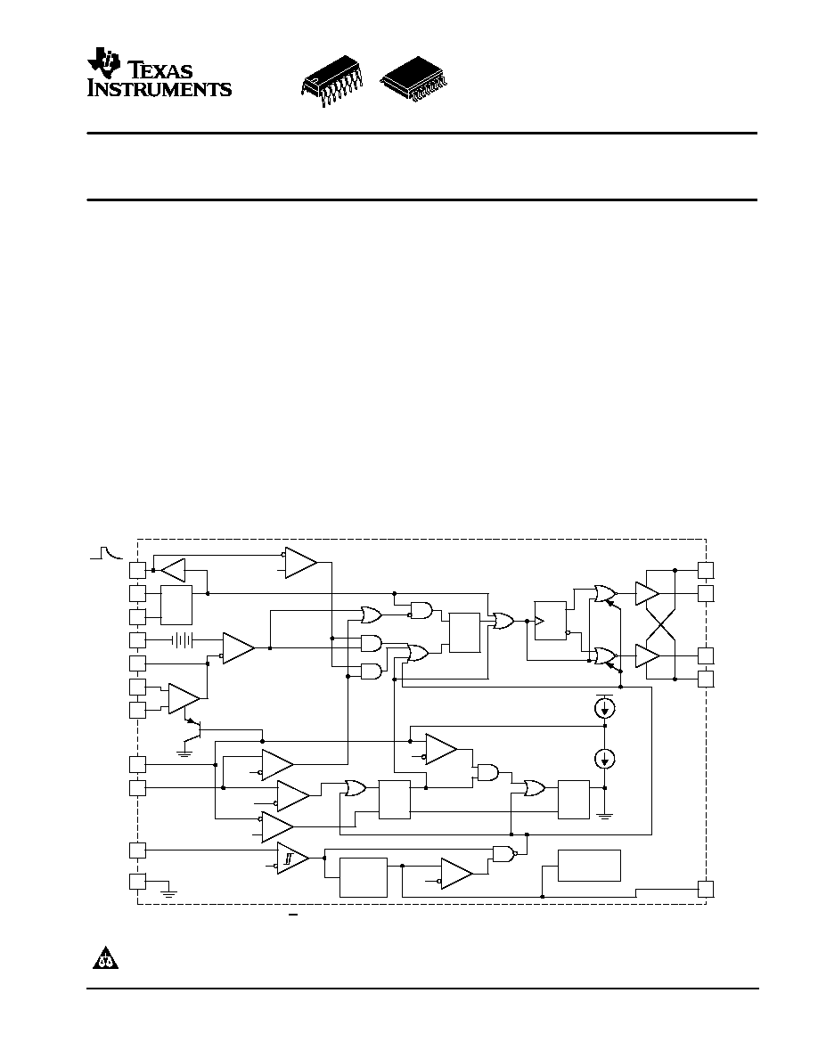
BLOCK DIAGRAM
4
5
6
7
3
2
1
OSC
CLK/LEB
RT
CT
RAMP
EAOUT
NI
INV
8
9
15
SS
ILIM
VCC
1.25 V
10
GND
(60%)
1.0 V
E/A
1.2 V
0.2 V
OVER CURRENT
CURRENT
LIMIT
R
SD
5 V
SOFT-START COMPLETE
R
SD
FAULT LATCH
RESTART
DELAY
T
13
11
14
VC
12
PWM
LATCH
9
m
A
250
m
A
R
S
*
RESTART
DELAY
LATCH
VREF
5.1 V
ON/OFF
UVLO
4 V
INTERNAL
BIAS
16
OUTA
OUTB
PGND
5.1 VREF
"B" 16V/10V
"A" 9.2V/8.4V
PWM COMPARATOR
UDG-02091
VREF GOOD
* On the UC1823A version, toggles Q and Q are always low.
Please be aware that an important notice concerning availability, standard warranty, and use in critical applications of Texas Instruments
semiconductor products and disclaimers thereto appears at the end of this data sheet.
www.ti.com
Copyright
2004, Texas Instruments Incorporated
PRODUCTION DATA information is current as of publication date. Products
conform to specifications per the terms of Texas Instruments standard warranty.
Production processing does not necessarily include testing of all parameters.
UC1823A, UC2823A, UC2823B,
UC3823A, UC3823B, UC1825A,
UC2825A, UC2825B, UC3825A, UC3825B
SLUS334C - AUGUST 1995 - REVISED AUGUST 2004
www.ti.com
2
These devices have limited built-in ESD protection. The leads should be shorted together or the device placed in conductive foam during
storage or handling to prevent electrostatic damage to the MOS gates.
DESCRIPTION (CONTINUED)
Functional improvements have also been implemented in this family. The UC3825 shutdown comparator is now a
high-speed overcurrent comparator with a threshold of 1.2 V. The overcurrent comparator sets a latch that ensures full
discharge of the soft-start capacitor before allowing a restart. While the fault latch is set, the outputs are in the low state.
In the event of continuous faults, the soft-start capacitor is fully charged before discharge to insure that the fault frequency
does not exceed the designed soft start period. The UC3825 CLOCK pin has become CLK/LEB. This pin combines the
functions of clock output and leading edge blanking adjustment and has been buffered for easier interfacing.
The UC3825A and UC3825B have dual alternating outputs and the same pin configuration of the UC3825. The UC3823A
and UC3823B outputs operate in phase with duty cycles from zero to less than 100%. The pin configuration of the UC3823A
and UC3823B is the same as the UC3823 except pin 11 is now an output pin instead of the reference pin to the current
limit comparator. "A" version parts have UVLO thresholds identical to the original UC3823 and UC3825. The "B" versions
have UVLO thresholds of 16 V and 10 V, intended for ease of use in off-line applications.
Consult the application note, The UC3823A,B and UC3825A,B Enhanced Generation of PWM Controllers, (SLUA125) for
detailed technical and applications information.
ORDERING INFORMATION
UVLO
TA
MAXIMUM
DUTY CYCLE
9.2 V / 8.4 V
16 V / 10 V
TA
MAXIMUM
DUTY CYCLE
SOIC-16(1)
(DW)
PDIP-16
(N)
PLCC-20(1)
(Q)
SOIC-16
(DW)
PDIP-16
(N)
PLCC-20(1)
(Q)
-40
∞
C to 85
∞
C
< 100%
UC2823ADW
UC2823AN
UC2823AQ
UC2823BDW
UC2823BN
-
-40
∞
C to 85
∞
C
< 50%
UC2825ADW
UC2825AN
UC2825AQ
UC2825BDW
UC2825BN
-
-0
∞
C to 70
∞
C
< 100%
UC3823ADW
UC3823AN
UC3823AQ
UC3823BDW
UC3823BN
-
-0
∞
C to 70
∞
C
< 50%
UC3825ADW
UC3825AN
UC3825AQ
UC3825BDW
UC3825BN
UC3825BQ
(1) The DW and Q packages are also available taped and reeled. Add TR suffix to the device type (i.e., UC2823ADWR). To order quantities of 1000
devices per reel for the Q package and 2000 devices per reel for the DW package.
UVLO
TA
MAXIMUM
DUTY CYCLE
9.2 V / 8.4 V
TA
MAXIMUM
DUTY CYCLE
CDIP-16
(J)
LCCC-20
(L)
-55
∞
C to 125
∞
C
< 100%
UC1823AJ, UC1823AJ883B, UC1823AJQMLV
UC1823AL, UC1823AL883B
-55
∞
C to 125
∞
C
< 50%
UC1825AJ, UC1825AJ883B, UC1825AJQMLV
UC1825AL, UC1825AL883B, UC1825ALQMLV
PIN ASSIGNMENTS
1
2
3
4
5
6
7
8
16
15
14
13
12
11
10
9
INV
NI
EAOUT
CLK/LEB
RT
CT
RAMP
SS
VREF
VCC
OUTB
VC
PGND
OUTA
GND
ILIM
DW, J, OR N PACKAGES
(TOP VIEW)
3
2
1 20 19
9 10 11 12 13
4
5
6
7
8
18
17
16
15
14
OUTB
VC
NC
PGND
OUTA
EAOUT
CLK/LEB
NC
RT
CT
Q OR L PACKAGES
(TOP VIEW)
NI
INV
NC
ILIM
GND
VREF
VCC
RAMP
SS
NC
NC = no connection

UC1823A, UC2823A, UC2823B,
UC3823A, UC3823B, UC1825A,
UC2825A, UC2825B, UC3825A, UC3825B
SLUS334C - AUGUST 1995 - REVISED AUGUST 2004
www.ti.com
3
TERMINAL FUNCTIONS
TERMINAL
NAME
NO.
I/O
DESCRIPTION
NAME
J or DW
Q or L
I/O
DESCRIPTION
CLK/LEB
4
5
O
Output of the internal oscillator
CT
6
8
I
Timing capacitor connection pin for oscillator frequency programming. The timing capacitor should
be connected to the device ground using minimal trace length.
EAOUT
3
4
O
Output of the error amplifier for compensation
GND
10
13
-
Analog ground return pin
ILIM
9
12
I
Input to the current limit comparator
INV
1
2
I
Inverting input to the error amplifier
NI
2
3
I
Non-inverting input to the error amplifier
OUTA
11
14
O
High current totem pole output A of the on-chip drive stage.
OUTB
14
18
O
High current totem pole output B of the on-chip drive stage.
PGND
12
15
-
Ground return pin for the output driver stage
RAMP
7
9
I
Non-inverting input to the PWM comparator with 1.25-V internal input offset. In voltage mode
operation, this serves as the input voltage feed-forward function by using the CT ramp. In peak
current mode operation, this serves as the slope compensation input.
RT
5
7
I
Timing resistor connection pin for oscillator frequency programming
SS
8
10
I
Soft-start input pin which also doubles as the maximum duty cycle clamp.
VC
13
17
-
Power supply pin for the output stage. This pin should be bypassed with a 0.1-
µ
F monolithic ceramic
low ESL capacitor with minimal trace lengths.
VCC
15
19
-
Power supply pin for the device. This pin should be bypassed with a 0.1-
µ
F monolithic ceramic low
ESL capacitor with minimal trace lengths
VREF
16
20
O
5.1-V reference. For stability, the reference should be bypassed with a 0.1-
µ
F monolithic ceramic
low ESL capacitor and minimal trace length to the ground plane.
ABSOLUTE MAXIMUM RATINGS
over operating free-air temperature range unless otherwise noted(1)
UNIT
VIN
Supply voltage,
VC, VCC
22 V
IO
Source or sink current, DC
OUTA, OUTB
0.5 A
IO
Source or sink current, pulse (0.5
µ
s)
OUTA, OUTB
2.2 A
Analog inputs
INV, NI, RAMP
-0.3 V to 7 V
Analog inputs
ILIM, SS
-0.3 V to 6 V
Power ground
PGND
±
0.2 V
ICLK
Clock output current
CLK/LEB
-5 mA
IO(EA)
Error amplifier output current
EAOUT
5 mA
ISS
Soft-start sink current
SS
20 mA
IOSC
Oscillator charging current
RT
-5 mA
TJ
Operating virtual junction temperature range
-55
∞
C to 150
∞
C
Tstg
Storage temperature
-65
∞
C to 150
∞
C
Lead temperature 1,6 mm (1/16 inch) from case for 10 seconds
-55C
∞
C to 150
∞
C
tSTG
Storage temperature
-65
∞
C to 150
∞
C
Lead temperature 1,6 mm (1/16 inch) from cases for 10 seconds
300
∞
C
(1) Stresses beyond those listed under "absolute maximum ratings" may cause permanent damage to the device. These are stress ratings only, and
functional operation of the device at these or any other conditions beyond those indicated under "recommended operating conditions" is not
implied. Exposure to absolute-maximum-rated conditions for extended periods may affect device reliability.
UC1823A, UC2823A, UC2823B,
UC3823A, UC3823B, UC1825A,
UC2825A, UC2825B, UC3825A, UC3825B
SLUS334C - AUGUST 1995 - REVISED AUGUST 2004
www.ti.com
4
ELECTRICAL CHARACTERISTICS
TA = -55
∞
C to 125
∞
C for the UC1823A/UC1825A, TA = -40
∞
C to 85
∞
C for the UC2823x/UC2825x, TA = 0
∞
C to 70
∞
C for the UC3823x/UC3825x,
RT = 3.65 k
, CT = 1 nF, VCC = 12 V, TA = TJ (unless otherwise noted)
PARAMETER
TEST CONDITIONS
MIN
TYP
MAX
UNIT
REFERENCE, VREF
VO
Ouput voltage range
TJ = 25
∞
C, IO = 1 mA
5.05
5.1
5.15
V
Line regulation
12 V
VCC
20 V
2
15
mV
Load regulation
1 mA
IO
10 mA
5
20
mV
Total output variation
Line, load, temperature
5.03
5.17
V
Temperature stability(1)
T(min) < TA < T(max)
0.2
0.4
mV/
∞
C
Output noise voltage(1)
10 Hz < f < 10 kHz
50
µ
VRMS
Long term stability(1)
TJ = 125
∞
C, 1000 hours
5
25
mV
Short circuit current
VREF = 0 V
30
60
90
mA
OSCILLATOR
fOSC
Initial accuracy(1)
TJ = 25
∞
C
375
400
425
kHz
fOSC
Initial accuracy(1)
RT = 6.6 k
, CT = 220 pF, TA = 25
∞
C
0.9
1
1.1
MHz
Total variation(1)
Line, temperature
350
450
kHz
Total variation(1)
RT = 6.6 k
, CT = 220 pF,
0.85
1.15
MHz
Voltage stability
12 V < VCC < 20 V
1%
Temperature stability(1)
T(min) < TA < T(max)
+/-
5%
High-level output voltage, clock
3.7
4
Low-level output voltage, clock
0
0.2
Ramp peak
2.6
2.8
3
V
Ramp valley
0.7
1
1.25
V
Ramp valley-to-peak
1.6
1.8
2
IOSC
Oscillator discharge current
RT = OPEN, VCT = 2 V
9
10
11
mA
ERROR AMPLIFIER
Input offset voltage
2
10
mV
Input bias current
0.6
3
A
Input offset current
0.1
1
µ
A
Open loop gain
1 V < VO < 4 V
60
95
CMRR
Common mode rejection ratio
1.5 V < VCM < 5.5 V
75
95
dB
PSRR
Power supply rejection ratio
12 V < VCC < 20 V
85
110
dB
IO(sink) Output sink current
VEAOUT = 1 V
1
2.5
mA
IO(src)
Output source current
VEAOUT = 4 V
-0.5
-1.3
mA
High-level output voltage
IEAOUT = -0.5 mA
4.5
4.7
5
V
Low-level output voltage
IEAOUT = -1 mA
0
0.5
1
V
Gain bandwidth product
f = 200 kHz
6
12
Mhz
Slew rate(1)
6
9
V/
µ
s
(1) Ensured by design. Not production tested.

UC1823A, UC2823A, UC2823B,
UC3823A, UC3823B, UC1825A,
UC2825A, UC2825B, UC3825A, UC3825B
SLUS334C - AUGUST 1995 - REVISED AUGUST 2004
www.ti.com
5
ELECTRICAL CHARACTERISTICS
TA = -55
∞
C to 125
∞
C for the UC1823A/UC1825A, TA = -40
∞
C to 85
∞
C for the UC2823x/UC2825x, TA = 0
∞
C to 70
∞
C for the UC3823x/UC3825x,
RT = 3.65 k
, CT = 1 nF, VCC = 12 V, TA = TJ (unless otherwise noted)
PWM COMPARATOR
IBIAS
Bias current, RAMP
VRAMP = 0 V
-1
-8
µ
A
Minimum duty cycle
0%
Maximum duty cycle
85%
tLEB
Leading edge blanking time
RLEB = 2 k
, CLEB = 470 pF
300
375
450
ns
RLEB
Leading edge blanking resistance
VCLK/LEB = 3 V
8.5
10.0
11.5
k
VZDC
Zero dc threshold voltage, EAOUT
VRAMP = 0 V
1.10
1.25
1.4
V
tDELAY Delay-to-output time
VEAOUT = 2.1 V, VILIM = 0 V to 2 V step
50
80
ns
CURRENT LIMIT / START SEQUENCE / FAULT
ISS
Soft-start charge current
VSS= 2.5 V
8
14
20
µ
A
VSS
Full soft-start threshold voltage
4.3
5
V
IDSCH
Restart discharge current
VSS= 2.5 V
100
250
350
µ
A
ISS
Restart threshold voltage
0.3
0.5
V
IBIAS
ILIM bias current
VILIM = 0 V to 2 V step
15
µ
A
ICL
Current limit threshold voltage
0.95
1
1.05
V
Overcurrent threshold voltage
1.14
1.2
1.26
V
td
Delay-to-output time, ILIM(1)
VILIM = 0 V to 2 V step
50
80
ns
OUTPUT
Low-level output saturation voltage
IOUT = 20 mA
0.25
0.4
Low-level output saturation voltage
IOUT = 200 mA
1.2
2.2
V
High-level output saturation voltage
IOUT = 20 mA
1.9
2.9
V
High-level output saturation voltage
IOUT = 200 mA
2
3
tr,
tf
Rise/fall time(1)
CL = 1 nF
20
45
ns
UNDERVOLTAGE LOCKOUT (UVLO)
UC2823B, UC2825B, UC3825B, UC3825B
16
17
Start threshold voltage
UC1823A, UC1825A, UC2823A, UC2825A
UC3825A, UC3825A
8.4
9.2
9.6
Stop threshold voltage
UC2823B, UC2825B, UC3825B, UC3825B
9
10
V
OVLO hysteresis
UC1823A, UC1825A, UC2823A, UC2825A
UC3825A, UC3825A
0.4
0.8
1.2
V
OVLO hysteresis
UC2823B, UC2825B, UC3825B, UC3825B
5
6
7
SUPPLY CURRENT
Isu
Startup current
VC = VCC = VTH = -0.5 V
100
300
µ
A
ICC
Input current
28
36
mA
(1) Ensured by design. Not production tested.