 | –≠–ª–µ–∫—Ç—Ä–æ–Ω–Ω—ã–π –∫–æ–º–ø–æ–Ω–µ–Ω—Ç: UC2827N-1 | –°–∫–∞—á–∞—Ç—å:  PDF PDF  ZIP ZIP |
www.ti.com
FEATURES
DESCRIPTION
RD
Q
S
20
DELAY
23
GND
11
VCC
REF
15
RT
17
CT
18
SYNC
19
CSA-
9
CSA+
8
SS
4
CSAO
7
CEA-
13
VEA-
16
VEA+
14
22
24
3
2
1
RAMP
CEA+
12
CEAO
VEAO
10
PULL
PGND
PUSH
SRC
BUCK
V+
DELAY
DELAY
T
Q
Q
REF
&
UVLO
SS
INHBT
UV
OSC
500 kHz
MAX
6
5
21
Current Sense
Amplifier
ILIM Comparator
+3 V
Current Error
Amplifier
PWM Comparator
0.7 V
Flying
Driver
Push/Pull
Drivers
OSC
UVLO
Voltage Error
Amplifier
+
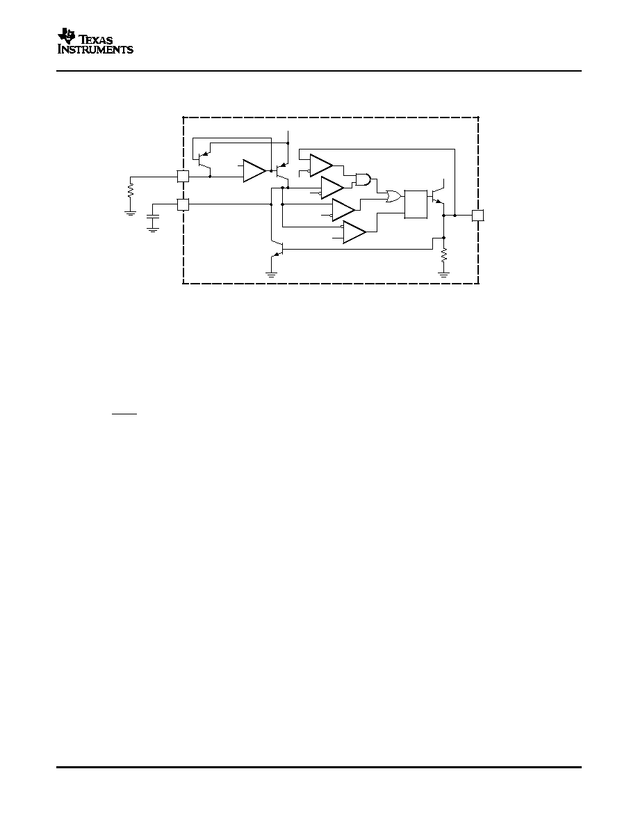
UC1827-1, UC1827-2
UC2827-1, UC2827-2
UC3827-1, UC3827-2
SLUS365A ≠ APRIL 1999 ≠ REVISED AUGUST 2005
BUCK CURRENT/VOLTAGE FED PUSH-PULL
PWM CONTROLLERS
∑
Ideal for Multiple Output and/or High
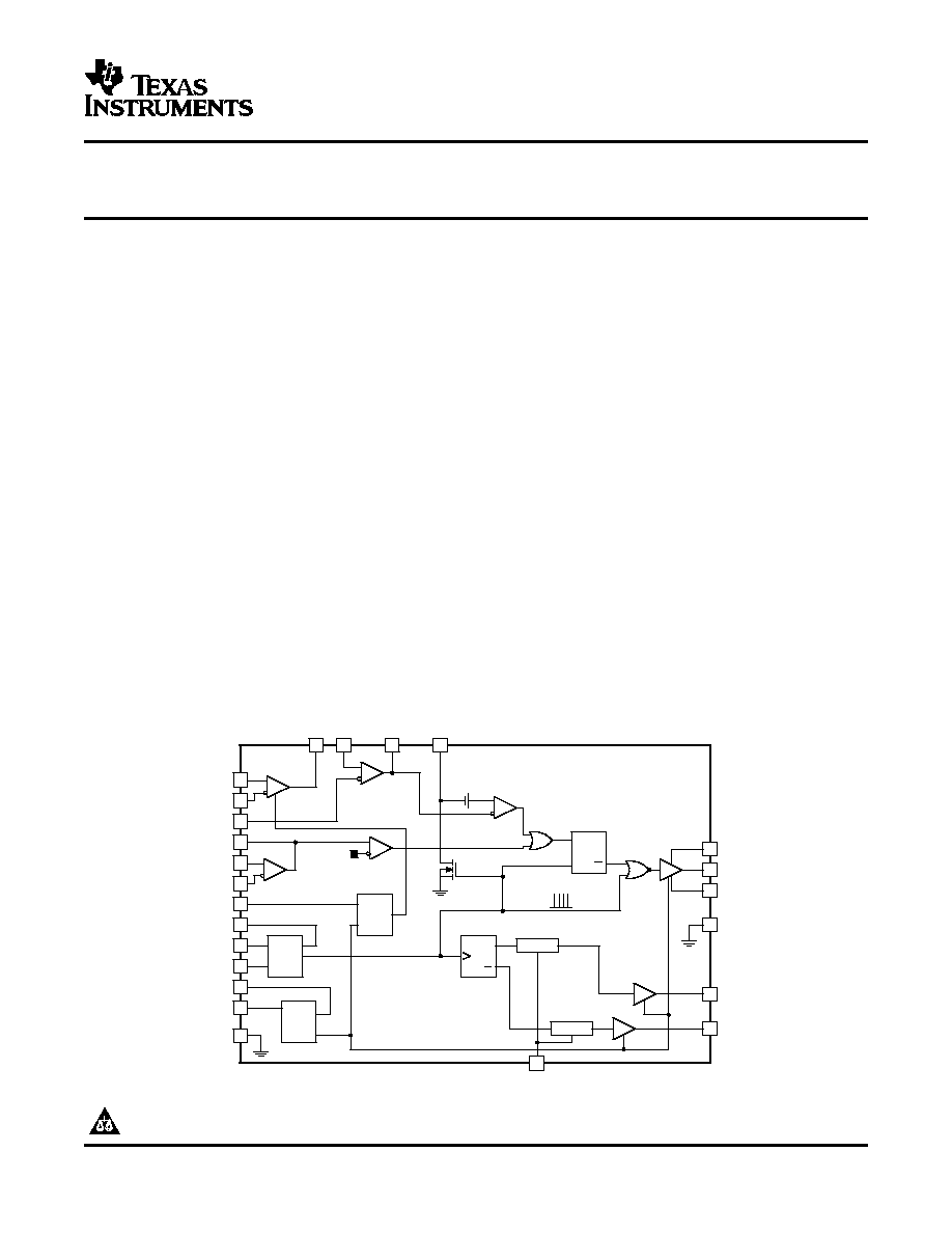
The UC3827 family of controller devices provides an
Voltage Output Voltage Converters
integrated control solution for cascaded buck and
push-pull converters. These converters are known as
∑
Up to 500 kHz Operation
current fed or voltage fed push-pull converters and
∑
High Voltage, High Current Floating
are ideally suited for multiple output and/or high
Driver for Buck Converter Stage
voltage output applications. In both current fed and
∑
UC3827-1 Current Fed Controller has
voltage fed modes, the push-pull switches are driven
Push-Pull Drivers with Overlapping
at 50% nominal duty cycles and at one half the
switching frequency of the buck stage. In the current
Conduction Periods
fed mode, the two switches are driven with a speci-
∑
UC3827-2 Voltage Fed Controller has
fied over-lap period to prevent ringing and voltage
Push-Pull Drivers with Nonoverlapping
stress on the devices. In the voltage fed mode, the
Conduction Periods
two switches are driven with a specified gap time
∑
Average Current Mode, Peak Current
between the switches to prevent shorting the trans-
Mode or Voltage Mode with Input
former across the energy storage capacitor and to
prohibit excessive currents flowing through the de-
Voltage Feedforward Control for Buck
vices.
Power Stage
∑
Wide Bandwidth, Low Offset,
The converter's output voltage is regulated by pulse
Differential Current Sense Amplifier
width modulation of the buck switch. The UC3827
contains complete protection and PWM control func-
∑
Precise Short Circuit Current Control
tions for the buck converter. Easy control of the
floating switch is accomplished by the floating drive
circuitry. The gate drive waveform is level shifted to
support an input voltage up to 72 V
DC
.
BLOCK DIAGRAM
Please be aware that an important notice concerning availability, standard warranty, and use in critical applications of Texas
Instruments semiconductor products and disclaimers thereto appears at the end of this data sheet.
PRODUCTION DATA information is current as of publication date.
Copyright © 1999≠2005, Texas Instruments Incorporated
Products conform to specifications per the terms of the Texas
Instruments standard warranty. Production processing does not
necessarily include testing of all parameters.
www.ti.com
DESCRIPTION (CONTINUED)
DISSIPATION RATINGS
UC1827-1, UC1827-2
UC2827-1, UC2827-2
UC3827-1, UC3827-2
SLUS365A ≠ APRIL 1999 ≠ REVISED AUGUST 2005
The UC3827 can be set up in traditional voltage mode control using input voltage feedforward technique or in
current mode control. Using current mode control prevents potential core saturation of the push-pull transformer
due to mismatches in timing and in component tolerances. With average current mode control, precise control of
the inductor current feeding the push-pull stage is possible without the noise sensitivity associated with peak
current mode control. The UC3827 average current mode loop can also be connected in parallel with the voltage
regulation loop to assist only in fault conditions.
Other valuable features of the UC3827 include bidirectional synchronization capability, user programmable
overlap time (UC3827-1), user programmable gap time (UC3827-2), a high bandwidth differential current sense
amplifier, and soft start circuitry.
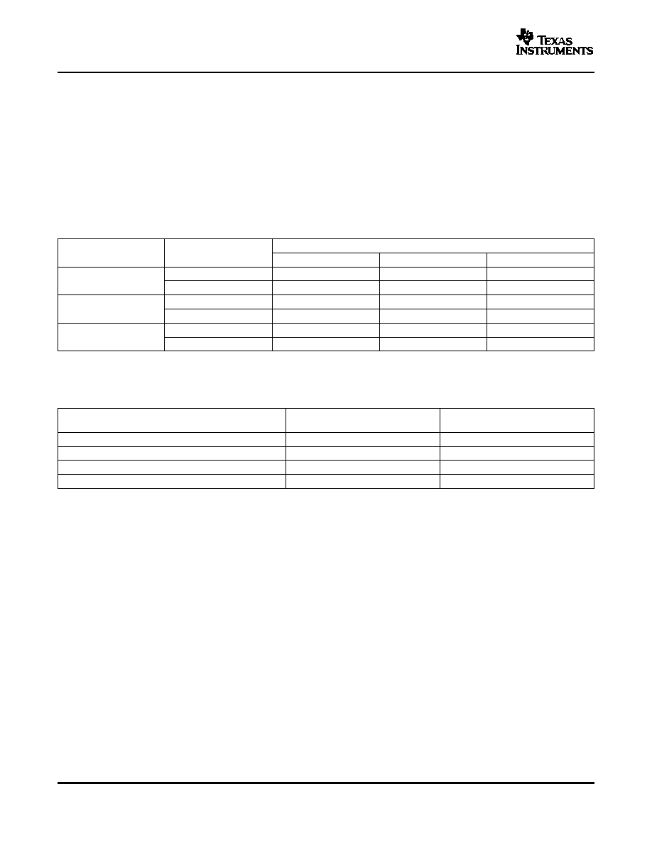
ORDERING INFORMATION
(1)
PACKAGES
T
A
= T
J
PUSH-PULL TOPOLOGY
SOIC-24
PDIP-24
PLCC-28
Current Fed
UC1827J-1
UC1827J-1
-55∞C to 125∞C
Voltage Fed
UC1827J-2
UC1827J-2
Current Fed
UC2827DW-1
UC2827N-1
-
-40∞C to 85∞C
Voltage Fed
UC2827DW-2
UC2827N-2
-
Current Fed
UC3827DW-1
UC3827N-1
UC3827Q-1
0∞C to 70∞C
Voltage Fed
UC3827DW-2
UC3827N-2
-
(1)
The DW and Q packages are also available taped and reeled. Add a TR suffix to the device type (i.e., UC2827DWTR-1).
PACKAGE
(
JA
) JUNCTION-TO-AMBIENT
(
JC
) JUNCTION-TO-WHAT?
TEMPERATURE (∞C/W)
TEMPERATURE (∞C/W)
24-pin (N)
60
(1)
30
24-pin (J)
70 to 90
28
(2)
28-pin (DW)
71 to 83
(3)
24
(3)
28-pin (QLCC)
40-65
(1)
30
(1)
Specified
JA
(junction-to-ambient) refers to devices mounted to 5-in
2
FR4 PC board with 1 oz. copper where noted. When a resistance
range is given, the lower values refer to a 5-in
2
aluminum PC board. The test PWB is 0.062 inches thick and typically used 0.635 mm
trace widths for power packages and 1.3 mm trace widths for non-power packages with a 100 ◊ 100 mil probe land area at the end of
each trace.
(2)
Specified
JC
(junction-to-what?) data values stated were derived from MIL-STD-1835B which states "The baseline values shown are
worst case (mean + 2s) for a 60 x 60 mil microcircuit device silicon die and applicable for devices with die sizes up to 14400 mils
2
. For
device sizes greater than 14400 mils
2
use the following values; dual-in-line, 11 ∞C/W; flat pack, 10 ∞C/W; pin grid array, 10 ∞C/W pin grid
array, 10 ∞C/W."
(3)
Modeled data. If there is a value range given for
JA
, the lower value refers to a 3 x 3 in., 1-oz, internal copper ground plane. The higher
value refers to a 1 x 1 in. ground plane. All model data assumes only one trace for each non-fused lead.
2

www.ti.com
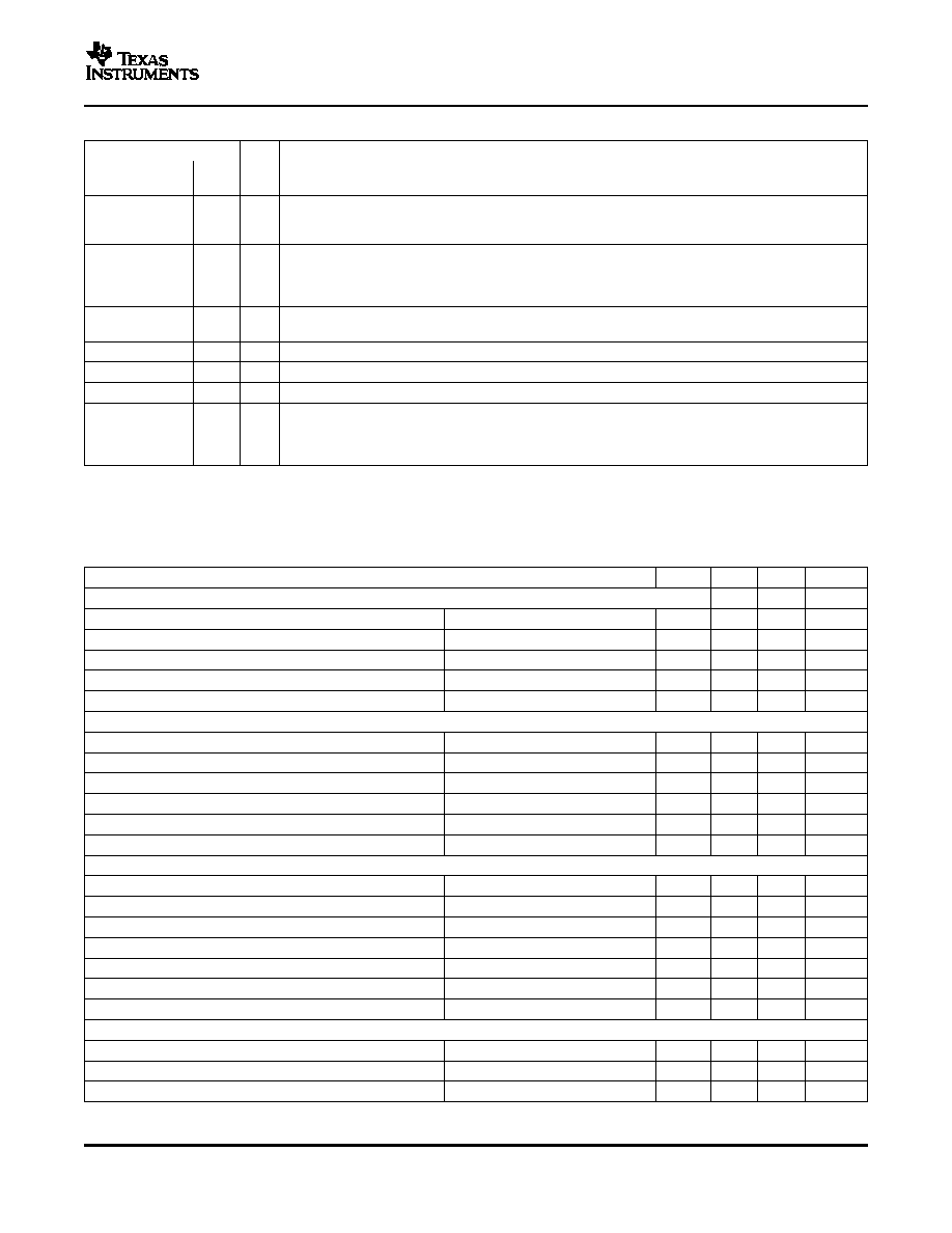
ABSOLUTE MAXIMUM RATINGS
(1)
CONNECTION DIAGRAMS
1
2
3
4
5
6
7
8
9
10
11
12
24
23
22
21
20
19
18
17
16
15
14
13
V+
BUCK
SRC
SS
RAMP
CEAO
CSAO
CSA+
CSA-
VEAO
GND
CEA+
PUSH
VCC
PULL
PGND
DELAY
SYNC
CT
RT
VEA-
REF
VEA+
CEA-
N, J OR DW PACKAGES
(TOP VIEW)
3 2 1
13 14
5
6
7
8
9
10
11
PGND
NC
NC
DELAY
SYNC
CT
RT
SS
RAMP
CEAO
CSAO
CSA+
CSA-
VEAO
4
15 16 17 18
CEA+
CEA-
VEA+
REF
NC
VEA-
SRC
BUCK
NC
V+
Q PACKAGE
(TOP VIEW)
28 27 26
25
24
23
22
21
20
19
12
GND
PUSH
VCC
PULL
NC - No internal connection
UC1827-1, UC1827-2
UC2827-1, UC2827-2
UC3827-1, UC3827-2
SLUS365A ≠ APRIL 1999 ≠ REVISED AUGUST 2005
UC2827-1
UC2827-2
UNITS
UC3827-1
UC3827-2
Supply voltage, VCC
20
CEAO, CEA+, CEA-, CSAO, CSA+, CSA-, CT, DELAY, PUSH, PULL,
≠0.3 to 5
RAMP, RT, SS, SYNC, VEA+, VEAO,
V
Input voltage range
V+ and BUCK
90
SRC
90-VCC
I/O continuous
±250
mA
BUCK driver
I/O peak
±1
A
I/O continuous
±200
mA
PUSH/PULL driver
I/O peak
±0.8
A
Storage temperature
≠65 to 150
Junction temperature
≠55 to 150
∞C
Lead temperature (soldering, 10 sec)
300
(1)
Voltages are referenced to ground. Currents are positive into, negative out of the specified terminal. Consult Packaging section of
databook for thermal limitations and considerations of packages.
PLCC-28 (Q PACKAGE)
(TOP VIEW)
DIL-24 (N or J, DW PACKAGES)
(TOP VIEW)
3

www.ti.com
(1)
f
OSC
+
0.77
R
RT
C
CT
(Hz)
(2)
t
DELAY
+
R
DELAY
200
W
10
*
9
(s)
(3)
I
RT
+
2.5 V
R
RT
UC1827-1, UC1827-2
UC2827-1, UC2827-2
UC3827-1, UC3827-2
SLUS365A ≠ APRIL 1999 ≠ REVISED AUGUST 2005
Terminal Functions
TERMINAL
I/O
DESCRIPTION
N or
NAME
Q
DW
Output of the buck PWM controller. The BUCK output is a floating driver, optimized for controlling the
BUCK
2
3
O
gate of an N-channel MOSFET. The peak sink and source currents are 1 A. V
CC
undervoltage faults
disables BUCK to an off condition (low).
CEA+
12
13
I
Non-inverting input of the current error amplifier.
CEA-
13
14
I
Inverting input of the current error amplifier
Output of the current error amplifier and the inverting input of the PWM comparator of the buck
CEAO
6
7
O
converter.
CSA+
8
9
I
Noninverting input of the current sense amplifier.
CSA≠
9
10
I
Inverting input of the current sense amplifier.
Output of the current sense amplifier and the noninverting input of the current limit comparator. When
the signal level on this pin exceeds the 3V threshold of the current limit comparator, the buck gate drive
CSAO
7
8
O
pulse is terminated. This feature is useful to implement cycle-by-cycle current limiting for the buck
converter.
Provides for the timing capacitor which is connected between CT and GND. The oscillator frequency is
set by CT and a resistor RT, connected between pin RT and GND. The CT discharge current is
CT
18
20
I
approximately 40 x the bias current through the resistor connected to RT. A practical maximum value for
the discharge current is 20 mA. The frequency of the oscillator is given by equation
(1)
A resistor to GND programs the overlap time of the PUSH and PULL outputs of the UC3827-1 and the
DELAY
20
22
I
dead time of the PUSH and PULL outputs of the UC3827-2. The minimum value of the resistor, R
DELAY
,
is 18 k
. The delay or overlap time is given by equation
(2)
Ground reference for all sensitive setup components not related to driving the outputs. They include all
GND
11
12
-
timing, voltage sense, current sense, and bypass components.
Ground connection for the PUSH and PULL outputs. PGND must be connected to GND at a single point
PGND
21
25
-
on the printed circuit board. This is imperative to prevent large, high frequency switching currents
flowing through the ground metalization inside the device.
Ground referenced output to drive an N-channel MOSFET. The PULL and the PUSH outputs are driving
PULL
22
26
O
the two switches of the push-pull converter with complementary signals at close to a 50% duty cycle.
Any undervoltage faults will disable PULL to an off condition (low).
Ground referenced output to drive an N-channel MOSFET. The PULL and the PUSH outputs are driving
PUSH
24
28
O
the two switches of the push-pull converter with complementary signals at close to a 50% duty cycle.
Any undervoltage faults disables PUSH to an off condition (low).
The RAMP voltage, after a 700 mV internal level shift, is fed to the noninverting input of the buck PWM
comparator. A resistor to V
IN
and a capacitor to GND provide an input voltage feedforward signal for the
buck controller in voltage mode control. In peak current mode control, the RAMP pin receives the
RAMP
5
6
I
current signal of the buck converter. In an average current mode setup, the RAMP pin has a linearly
increasing ramp signal. This waveform may be generated either by connecting RAMP directly to CT, or
by connecting both a resistor from VCC to RAMP and a capacitor from RAMP to GND.
The output of the +5V on board reference. Bypass this pin with a capacitor to GND. The reference is off
REF
15
16
O
when the chip is in undervoltage lockout mode.o
A resistor to GND programs the charge current of the timing capacitor connected to CT. The charge
current approximately equals that shown in equation
(3)
. The charge current should be less than 500 µA
RT
17
19
I
to keep CT's discharge peak current less than 20 mA, which is CT's maximum practical discharge value.
The discharge time, which sets the maximum duty cycle, is set internally and is influenced by the charge
current.
The source connection for the floating buck switch. The voltage on the SRC pin can exceed VCC but
SRC
3
4
I
must be lower than 90 V≠V
VCC
. Also, during turn-off transients of the buck switch, the voltage at SRC
can go to ≠2V.
4
www.ti.com
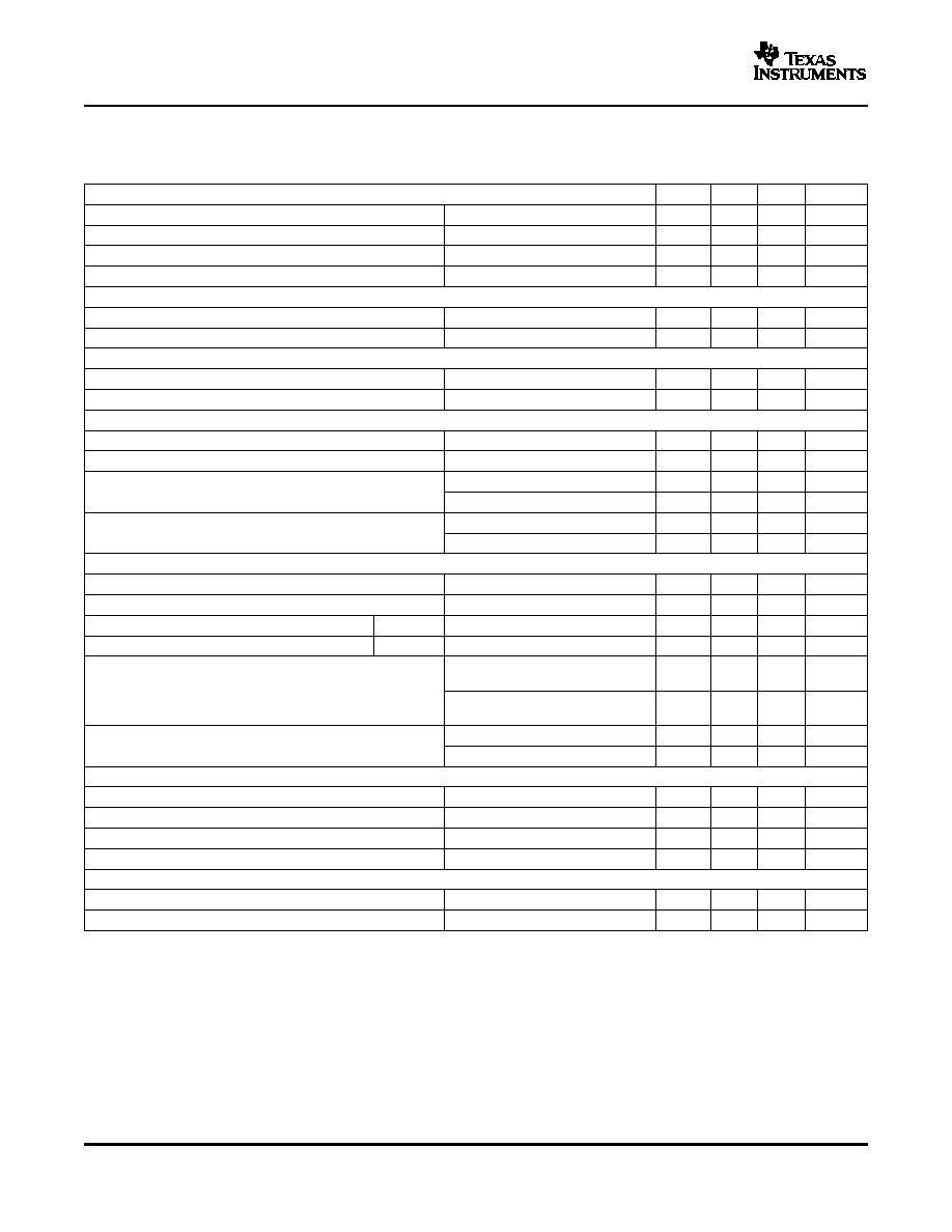
ELECTRICAL CHARACTERISTICS
UC1827-1, UC1827-2
UC2827-1, UC2827-2
UC3827-1, UC3827-2
SLUS365A ≠ APRIL 1999 ≠ REVISED AUGUST 2005
Terminal Functions (continued)
TERMINAL
I/O
DESCRIPTION
N or
NAME
Q
DW
5Soft-start pin requires a capacitor to GND. During soft-start the output of the voltage error amplifier is
SS
4
5
O
clamped to the soft-start capacitor voltage which is slowly charged by an internal current source. In
UVLO, SS is held low.
A bidirectional pin for the oscillator., used to synchronize several chips to the fastest oscillator. Its input
synchronization threshold is 1.4 V. The SYNC voltage is 3.6 V when the oscillator capacitor, CT, is
SYNC
19
21
I
discharged. Otherwise it is 0 V. If the recommended synchronization circuit is not used, a 1 k
or lower
value resistor from SYNC to GND may be needed to increase the fall time of the signal at SYNC.
A voltage source connected to this pin supplies the power for the UC3827. It is recommended to bypass
VCC
23
27
I
this pin to both GND and PGND ground connections with good quality high frequency capacitors
VEA+
14
15
I
Non-inverting input of the voltage error amplifier
VEA-
16
18
I
Inverting input of the voltage error amplifier
VEAO
10
11
O
Output of the voltage error amplifier
Supply voltage for the buck output. The floating driver of the UC3827 uses the bootstrap technique
which requires a reservoir capacitor to store the required energy for the on time of the buck switch. A
V+
1
1
I
diode must be connected from VCC to V+ to charge the reservoir capacitor. This diode must be able to
withstand V
IN
. The reservoir capacitor must be connected between V+ and SRC.
Unless otherwise spsecified, V
VCC
= 15 V, V
V+
= 14.3 V, C
CT
= 340 pF, R
RT
= 10 k
, R
DELAY
= 24.3 k
, V
SRC
= V
GND
= V
BUCK
=
V
PUSH
= V
PULL
outputs no load, T
J
= T
A
PARAMETER
TEST CONDITIONS
MIN
TYP
MAX
UNIT
SUPPLY
VCC UVLO, Turn-on
8.3
8.8
9.5
V
Hysteresis
0.9
1.2
1.5
V
I
VCC
Supply current start
V
VCC
= 8 V
1000
µA
I
VCC
Supply current run
32
45
mA
I
V+
buck high
0.2
1
2
mA
VOLTAGE ERROR AMPLIFIER
IB
0.5
3
µA
VIO
10
mV
AVOL
80
95
dB
GBW
(1)
Gain bandwidth
1
4
MHz
V
OL
Low-level output voltage
I
VEAO
= 0 µA (No load)
0.3
0.5
V
V
OH
High-level output voltage
I
VEAO
= 0 µA (No load)
2.85
3
3.20
V
CURRENT SENSE AMPLIFIER
IB
≠1
≠5
µA
VIO
5
mV
AVOL
80
110
dB
GBW
(1)
Gain bandwidth
15
29
MHz
V
OL
Low-level output voltage
I
CEAO
= 0 µA (No load)
0.25
0.5
V
V
OH
High-level output voltage
I
CEAO
= 0 µA (No load)
3
3.3
V
CMRR
Common mode range
(1)
-0.3
2
V
CURRENT ERROR AMPLIFIER
IB
≠1
≠5
µA
VIO
10
mV
AVOL
80
110
dB
(1)
Ensured by design. Not production tested.
5
www.ti.com
UC1827-1, UC1827-2
UC2827-1, UC2827-2
UC3827-1, UC3827-2
SLUS365A ≠ APRIL 1999 ≠ REVISED AUGUST 2005
ELECTRICAL CHARACTERISTICS (continued)
Unless otherwise spsecified, V
VCC
= 15 V, V
V+
= 14.3 V, C
CT
= 340 pF, R
RT
= 10 k
, R
DELAY
= 24.3 k
, V
SRC
= V
GND
= V
BUCK
=
V
PUSH
= V
PULL
outputs no load, T
J
= T
A
PARAMETER
TEST CONDITIONS
MIN
TYP
MAX
UNIT
GBW
(1)
Gain bandwidth
At 100 kHz, Measure Gain
2
4.5
MHz
V
OL
I
CEAO
= 0 µA (No Load)
0.25
0.5
V
V
OH
I
CEAO
= 0 µA (No Load)
3.3
3.5
V
CMRR
Common mode range
(1)
-0.3
5
V
OSCILLATOR SECTION
f
OSC
Frequency
180
220
250
kHz
I
CT(dsch)
CT discharge current
3.5V at CT when CT removed
5
mA
PWM COMPARATOR
D
MAX
Minimum duty cycle
200 kHz
0%
D
MAX
Maximum duty cycle
200 kHz
85%
91%
95%
BUCK OUTPUT STAGE
t
RISE
Rise time
1 nF Load
(2)
40
100
ns
t
FALL
Fall tIme
1 nF, Load
30
80
ns
I
BUCK
= ≠15 mA , V+ ≠BUCK
(3)
1.5
2.5
V
V
OH
High-level output voltage
IBUCK = ≠150 mA, V+ ≠BUCK
(3)
2
2.5
V
I
BUCK
= 15 mA
(4)
0.2
0.4
V
V
OL
Low-level output voltage
I
BUC
K = 150 mA
(4)
0.7
1.2
V
PUSH/PULL OUTPUT STAGES
t
RISE
Rise time
1 nF load
50
100
ns
t
FALL
Fall tIme
1 nF load
35
100
ns
Overlap time
UCx827-1
1 nF loads
(5)
100
250
400
ns
Nonoverlapping time
(6)
UCx827-2
100
250
500
ns
I
PUSH/PULL
= ≠10 mA, VCC ≠ PUSH
2
3
V
(7)
V
OH
High-level output voltage
I
PUSH/PULL
= ≠100 mA, VCC ≠
2.5
3
V
PUSH
(7)
I
PUSH/PULL
= 10 mA
(7)
0.2
0.8
V
V
OL
Low-level output voltage
I
PUSH/PULL
= 100 mA
(7)
0.6
1.2
V
REFERENCE
Reference voltage
4.8
5
5.2
V
I
SC
Shor-circuit current
V
REF
= 0V
≠35
≠50
≠65
mA
Line regulation
0.5V < V
VCC
< 20 V
5
20
mV
Load regulation
0 mA < I
IO
< 10 mA
8
20
mV
SOFT START
V
OL
Low-level output voltage saturation
V
VCC
= 7 V
250
500
mV
I
SS
Soft-start current
≠5
≠12
≠25
µA
(2)
Measure the rise time from when BUCK crosses 1 V until it crosses 9 V.
(3)
To force BUCK high, force V
CSAO
=2.5 V, V
CEAO
= 2.5 V, a 25-k
pulldown resistor from RAMP to ground, and V
CT
= 0.5 V.
(4)
To force BUCK low, force V
CSAO
= 2.5 V, V
CEAO
= 2.5 V, a 10-k
pulldown resistor from RAMP to ground, and V
CT
= 3.5 V.
(5)
The overlap time is measured from the point at which the rising edge of PUSH/PULL crosses 5 V until the falling edge of PULL/PUSH
crosses 5V.
(6)
The non-overlap time is measured from the point at which the falling edge of PUSH/PULL crosses 5 V until the rising edge of
PULL/PUSH crosses 5 V.
(7)
To toggle PUSH or PULL into a desired state, pulse CT from 0.5 V to 3.5 V. PUSH and PULL toggle on the rising edge of CT.
6
www.ti.com
APPLICATION INFORMATION
+
≠
RT
CT
SYNC
S
R
V
REF
2.5 V
OSCILLATOR
V
REF
10 k
W
1.4 V
2.5 V
2.9 V
0.5 V
R
T
C
T
VDG-99086
CIRCUIT BLOCK DESCRIPTION
PWM Oscillator
I
RT
+
2.5 V
R
RT
(1)
UC1827-1, UC1827-2
UC2827-1, UC2827-2
UC3827-1, UC3827-2
SLUS365A ≠ APRIL 1999 ≠ REVISED AUGUST 2005
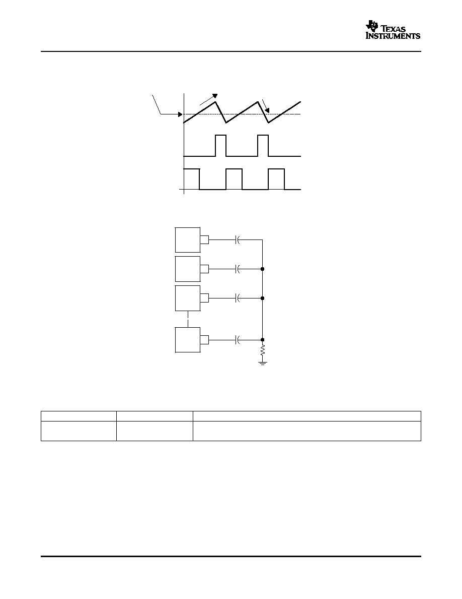
Figure 1. Oscillator Block With External Connections
The oscillator block diagram with external connections is shown in
Equation 1
. A resistor (R
T
) connected to pin
RT sets the linear charge current:
The timing capacitor (C
CT
) is linearly charged with the charge current forcing the OSC pin to charge to a 3.4 V
threshold. After exceeding this threshold, the RS flip-flop is set driving CLKSYN high and R
DEAD
low which
discharges C
CT
. CT continues to discharge until it reaches a 0.5 V threshold and resets the RS flip-flop which
repeats the charging sequence as shown in
Figure 2
As shown in
Figure 3
, several oscillators are synchronized to the highest free running frequency by connecting
100 pF capacitors in series with each CLKSYN pin and connecting the other side of the capacitors together
forming the CLKSYN bus. The CLKSYN bus is then pulled down to ground with a resistance of approximately
10k. Referring to
Figure 1
, the synchronization threshold is 1.4 V. The oscillator blanks any synchronization pulse
that occurs when OSC is below 2.5 V. This allows units, once they discharge below 2.5 V, to continue through
the current discharge and subsequent charge cycles whether or not other units on the CLKSYN bus are still
synchronizing. This requires the frequency of all free running oscillators to be within 17% of each other to assure
synchronization.
7
www.ti.com
OSC
CLKSYN
OUT
THRESHOLD
Charging
VAO Current
Command
Discharging
Threshold
2.9 V
0.5 V
3.6 V
1.4 V
8.5 V
0 V
VDG-99087
C
L
K
S
Y
N
B
U
S
OSC1
OSC2
OSC3
OSC10
SYNC
SYNC
SYNC
SYNC
100 pF
100 pF
100 pF
100 pF
10 k
W
VDG-99085
REVISION HISTORY
UC1827-1, UC1827-2
UC2827-1, UC2827-2
UC3827-1, UC3827-2
SLUS365A ≠ APRIL 1999 ≠ REVISED AUGUST 2005
APPLICATION INFORMATION (continued)
Figure 2. Oscillator and PWM Output Waveform
Figure 3. Oscillator Synchronization Connection Diagram
REVISION
DATE OF CHANGE
DESCRIPTION
Improved CMRR of CSA from ( 0 - 2 V) to ( -0.3 - 2 V)
SLUS365A
8/2005
Improved CMRR of CEA from ( 0 - 5 V) to ( -0.3 - 5 V)
8
PACKAGING INFORMATION
Orderable Device
Status
(1)
Package
Type
Package
Drawing
Pins Package
Qty
Eco Plan
(2)
Lead/Ball Finish
MSL Peak Temp
(3)
UC1827J-1
OBSOLETE
CDIP
J
24
TBD
Call TI
Call TI
UC1827L-1
OBSOLETE
TO/SOT
L
20
TBD
Call TI
Call TI
UC2827DW-1
ACTIVE
SOIC
DW
24
25
Green (RoHS &
no Sb/Br)
CU NIPDAU
Level-3-260C-168 HR
UC2827DW-2
ACTIVE
SOIC
DW
24
25
Green (RoHS &
no Sb/Br)
CU NIPDAU
Level-3-260C-168 HR
UC2827DW-2G4
ACTIVE
SOIC
DW
24
25
Green (RoHS &
no Sb/Br)
CU NIPDAU
Level-3-260C-168 HR
UC2827DWTR-1
ACTIVE
SOIC
DW
24
2000 Green (RoHS &
no Sb/Br)
CU NIPDAU
Level-3-260C-168 HR
UC2827DWTR-2
ACTIVE
SOIC
DW
24
2000
TBD
CU NIPDAU
Level-3-235C-168 HR
UC2827N-1
ACTIVE
PDIP
N
24
15
TBD
Call TI
Level-NA-NA-NA
UC2827N-2
ACTIVE
PDIP
N
24
15
TBD
Call TI
Level-NA-NA-NA
UC3827DW-1
ACTIVE
SOIC
DW
24
25
Green (RoHS &
no Sb/Br)
CU NIPDAU
Level-3-260C-168 HR
UC3827DW-1G4
ACTIVE
SOIC
DW
24
25
Green (RoHS &
no Sb/Br)
CU NIPDAU
Level-3-260C-168 HR
UC3827DW-2
ACTIVE
SOIC
DW
24
25
Green (RoHS &
no Sb/Br)
CU NIPDAU
Level-3-260C-168 HR
UC3827DWTR-1
ACTIVE
SOIC
DW
24
2000 Green (RoHS &
no Sb/Br)
CU NIPDAU
Level-3-260C-168 HR
UC3827DWTR-1G4
ACTIVE
SOIC
DW
24
2000 Green (RoHS &
no Sb/Br)
CU NIPDAU
Level-3-260C-168 HR
UC3827DWTR-2
ACTIVE
SOIC
DW
24
2000 Green (RoHS &
no Sb/Br)
CU NIPDAU
Level-3-260C-168 HR
UC3827DWTR-2G4
ACTIVE
SOIC
DW
24
2000 Green (RoHS &
no Sb/Br)
CU NIPDAU
Level-3-260C-168 HR
UC3827N-1
ACTIVE
PDIP
N
24
15
TBD
Call TI
Level-NA-NA-NA
UC3827N-2
ACTIVE
PDIP
N
24
15
TBD
Call TI
Level-NA-NA-NA
(1)
The marketing status values are defined as follows:
ACTIVE: Product device recommended for new designs.
LIFEBUY: TI has announced that the device will be discontinued, and a lifetime-buy period is in effect.
NRND: Not recommended for new designs. Device is in production to support existing customers, but TI does not recommend using this part in
a new design.
PREVIEW: Device has been announced but is not in production. Samples may or may not be available.
OBSOLETE: TI has discontinued the production of the device.
(2)
Eco
Plan
-
The
planned
eco-friendly
classification:
Pb-Free
(RoHS)
or
Green
(RoHS
&
no
Sb/Br)
-
please
check
http://www.ti.com/productcontent
for the latest availability information and additional product content details.
TBD: The Pb-Free/Green conversion plan has not been defined.
Pb-Free (RoHS): TI's terms "Lead-Free" or "Pb-Free" mean semiconductor products that are compatible with the current RoHS requirements
for all 6 substances, including the requirement that lead not exceed 0.1% by weight in homogeneous materials. Where designed to be soldered
at high temperatures, TI Pb-Free products are suitable for use in specified lead-free processes.
Green (RoHS & no Sb/Br): TI defines "Green" to mean Pb-Free (RoHS compatible), and free of Bromine (Br) and Antimony (Sb) based flame
retardants (Br or Sb do not exceed 0.1% by weight in homogeneous material)
(3)
MSL, Peak Temp. -- The Moisture Sensitivity Level rating according to the JEDEC industry standard classifications, and peak solder
temperature.
Important Information and Disclaimer:The information provided on this page represents TI's knowledge and belief as of the date that it is
PACKAGE OPTION ADDENDUM
www.ti.com
17-Nov-2005
Addendum-Page 1

provided. TI bases its knowledge and belief on information provided by third parties, and makes no representation or warranty as to the
accuracy of such information. Efforts are underway to better integrate information from third parties. TI has taken and continues to take
reasonable steps to provide representative and accurate information but may not have conducted destructive testing or chemical analysis on
incoming materials and chemicals. TI and TI suppliers consider certain information to be proprietary, and thus CAS numbers and other limited
information may not be available for release.
In no event shall TI's liability arising out of such information exceed the total purchase price of the TI part(s) at issue in this document sold by TI
to Customer on an annual basis.
PACKAGE OPTION ADDENDUM
www.ti.com
17-Nov-2005
Addendum-Page 2
MECHANICAL DATA
MCDI004A ≠ JANUARY 1995 ≠ REVISED NOVEMBER 1997
POST OFFICE BOX 655303
∑
DALLAS, TEXAS 75265
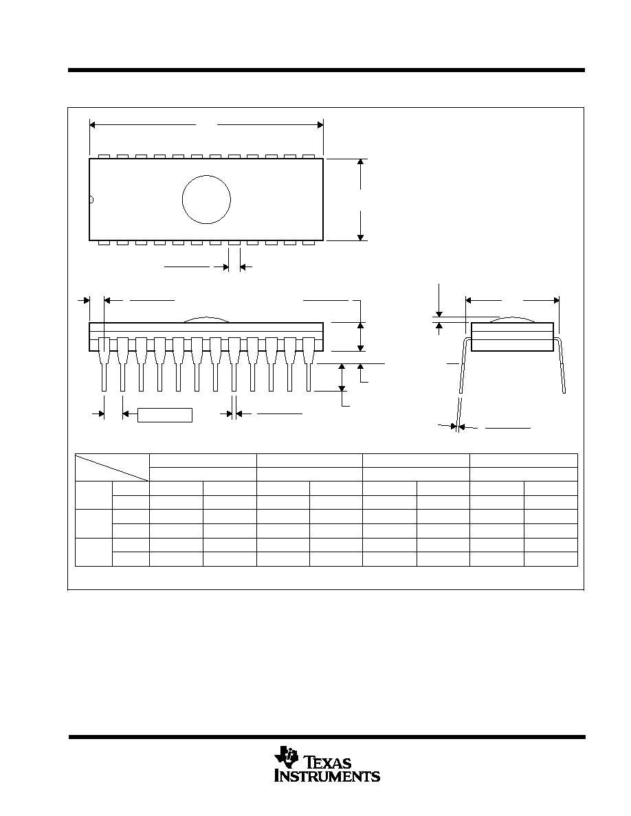
J (R-GDIP-T**)
CERAMIC DUAL-IN-LINE PACKAGE
24 PINS SHOWN
A
C
0.018 (0,46) MIN
Seating Plane
0.010 (0.25) MAX
Lens Protrusion (Lens Optional)
WIDE
NARR
WIDE
32
NARR
WIDE
0.125 (3,18) MIN
0.514(13,06) 0.571(14,50)
0.541(13,74) 0.598(15,19)
1.668(42,37) 1.668(42,37)
1.632(41,45) 1.632(41,45)
0.590(14,99) 0.590(14,99)
0.624(15,85) 0.624(15,85)
4040084/C 10/97
0.012 (0,30)
0.008 (0,20)
40
0.624(15,85) 0.624(15,85)
0.590(14,99) 0.590(14,99)
2.032(51,61) 2.032(51,61)
2.068(52,53) 2.068(52,53)
0.541(13,74) 0.598(15,19)
0.514(13,06) 0.571(14,50)
B
13
12
0.090 (2,29)
0.060 (1,53)
0.045 (1,14)
0.065 (1,65)
24
1
28
0.022 (0,56)
0.014 (0,36)
NARR
24
NARR
WIDE
0.624(15,85) 0.624(15,85)
0.590(14,99) 0.590(14,99)
1.235(31,37) 1.235(31,37)
1.265(32,13) 1.265(32,13)
0.541(13,74) 0.598(15,19)
0.514(13,06) 0.571(14,50)
"A"
DIM
"B"
"C"
PINS **
MAX
MIN
MIN
MAX
MAX
MIN
0.514(13,06) 0.571(14,50)
0.541(13,74) 0.598(15,19)
1.465(37,21) 1.465(37,21)
1.435(36,45) 1.435(36,45)
0.590(14,99) 0.590(14,99)
0.624(15,85) 0.624(15,85)
0.175 (4,45)
0.140 (3,56)
0.100 (2,54)
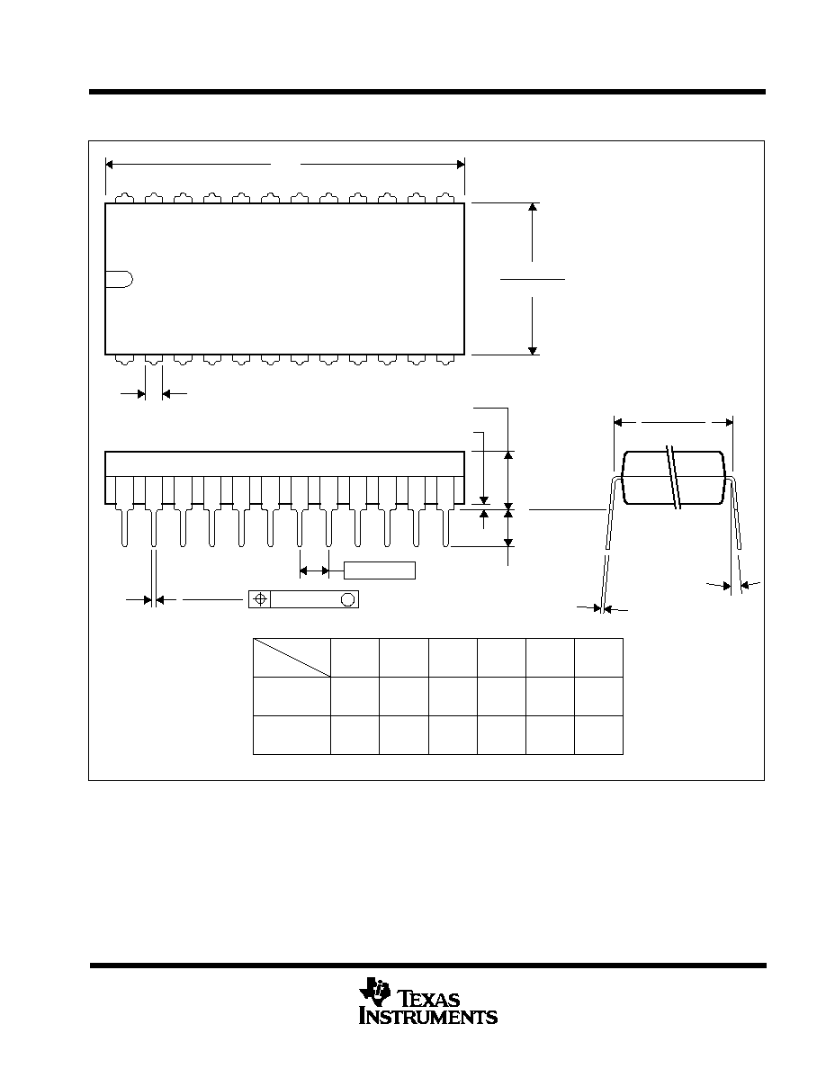
NOTES: A. All linear dimensions are in inches (millimeters).
B. This drawing is subject to change without notice.
C. Window (lens) added to this group of packages (24-, 28-, 32-, 40-pin).
D. This package can be hermetically sealed with a ceramic lid using glass frit.
E. Index point is provided on cap for terminal identification.

MECHANICAL DATA
MPDI006B ≠ SEPTEMBER 2001 ≠ REVISED APRIL 2002
POST OFFICE BOX 655303
∑
DALLAS, TEXAS 75265
N (R≠PDIP≠T24)
PLASTIC DUAL≠IN≠LINE
0.020 (0,51) MIN
0.021 (0,53)
0.015 (0,38)
0.100 (2,54)
1
24
0.070 (1,78) MAX
12
13
1.222 (31,04) MAX
0.125 (3,18) MIN
0'≠15'
0.010 (0,25) NOM
0.425 (10,80) MAX
Seating Plane
0.200 (5,08) MAX
0.360 (9,14) MAX
0.010 (0,25)
4040051≠3/D 09/01
NOTES: A. All linear dimensions are in inches (millimeters).
B. This drawing is subject to change without notice.
C. Falls within JEDEC MS≠010
MECHANICAL DATA
MPDI008 ≠ OCTOBER 1994
POST OFFICE BOX 655303
∑
DALLAS, TEXAS 75265
N (R-PDIP-T**)
PLASTIC DUAL-IN-LINE PACKAGE
24 PIN SHOWN
12
Seating Plane
0.560 (14,22)
0.520 (13,21)
13
0.610 (15,49)
0.590 (14,99)
52
48
40
0.125 (3,18) MIN
2.390
(60,71)
(62,23)
(53,09)
(51,82)
2.040
2.090
2.450
2.650
(67,31)
(65,79)
2.590
0.010 (0,25) NOM
4040053 / B 04/95
A
0.060 (1,52) TYP
1
24
32
28
24
1.230
(31,24)
(32,26)
(36,83)
(35,81)
1.410
1.450
1.270
PINS **
DIM
0.015 (0,38)
0.021 (0,53)
A MIN
A MAX
1.650
(41,91)
(40,89)
1.610
0.020 (0,51) MIN
0.200 (5,08) MAX
0.100 (2,54)
M
0.010 (0,25)
0
∞
≠ 15
∞
NOTES: A. All linear dimensions are in inches (millimeters).
B. This drawing is subject to change without notice.
C. Falls within JEDEC MS-011
D. Falls within JEDEC MS-015 (32 pin only)


IMPORTANT NOTICE
Texas Instruments Incorporated and its subsidiaries (TI) reserve the right to make corrections, modifications,
enhancements, improvements, and other changes to its products and services at any time and to discontinue
any product or service without notice. Customers should obtain the latest relevant information before placing
orders and should verify that such information is current and complete. All products are sold subject to TI's terms
and conditions of sale supplied at the time of order acknowledgment.
TI warrants performance of its hardware products to the specifications applicable at the time of sale in
accordance with TI's standard warranty. Testing and other quality control techniques are used to the extent TI
deems necessary to support this warranty. Except where mandated by government requirements, testing of all
parameters of each product is not necessarily performed.
TI assumes no liability for applications assistance or customer product design. Customers are responsible for
their products and applications using TI components. To minimize the risks associated with customer products
and applications, customers should provide adequate design and operating safeguards.
TI does not warrant or represent that any license, either express or implied, is granted under any TI patent right,
copyright, mask work right, or other TI intellectual property right relating to any combination, machine, or process
in which TI products or services are used. Information published by TI regarding third-party products or services
does not constitute a license from TI to use such products or services or a warranty or endorsement thereof.
Use of such information may require a license from a third party under the patents or other intellectual property
of the third party, or a license from TI under the patents or other intellectual property of TI.
Reproduction of information in TI data books or data sheets is permissible only if reproduction is without
alteration and is accompanied by all associated warranties, conditions, limitations, and notices. Reproduction
of this information with alteration is an unfair and deceptive business practice. TI is not responsible or liable for
such altered documentation.
Resale of TI products or services with statements different from or beyond the parameters stated by TI for that
product or service voids all express and any implied warranties for the associated TI product or service and
is an unfair and deceptive business practice. TI is not responsible or liable for any such statements.
Following are URLs where you can obtain information on other Texas Instruments products and application
solutions:
Products
Applications
Amplifiers
amplifier.ti.com
Audio
www.ti.com/audio
Data Converters
dataconverter.ti.com
Automotive
www.ti.com/automotive
DSP
dsp.ti.com
Broadband
www.ti.com/broadband
Interface
interface.ti.com
Digital Control
www.ti.com/digitalcontrol
Logic
logic.ti.com
Military
www.ti.com/military
Power Mgmt
power.ti.com
Optical Networking
www.ti.com/opticalnetwork
Microcontrollers
microcontroller.ti.com
Security
www.ti.com/security
Telephony
www.ti.com/telephony
Video & Imaging
www.ti.com/video
Wireless
www.ti.com/wireless
Mailing Address:
Texas Instruments
Post Office Box 655303 Dallas, Texas 75265
Copyright
2005, Texas Instruments Incorporated