 | –≠–ª–µ–∫—Ç—Ä–æ–Ω–Ω—ã–π –∫–æ–º–ø–æ–Ω–µ–Ω—Ç: UC282-x | –°–∫–∞—á–∞—Ç—å:  PDF PDF  ZIP ZIP |
Document Outline
- features
- description
- block diagram
- absolute maximum ratings over operating free-air temperature (unless otherwise noted)Å
- electrical characteristics, TA = -40∞C to 100∞C for the UC282-X series and 0∞C to 100∞C for the
UC382-X, VB = 5 V, VIN = 3.3 V, VOUT = 2.5 V for the UC382-ADJ, TA = TJ, (unless otherwise stated)
- UC382-3 fixed 2.5 V, 3-A family
- UC382-2 fixed 2.1 V, 3-A family
- UC382-1 fixed 1.5 V, 3-A family
- UC382-ADJ adjustable, 3-A family
- pin descriptions
- APPLICATION INFORMATION
UC282 1, UC282 2, UC282 3, UC282 ADJ, UC382 1, UC382 2, UC382 3, UC382 ADJ
FAST LDO LINEAR REGULATOR
SLUS317B - JANUARY 2000 - REVISED FEBRUARY 2004
1
POST OFFICE BOX 655303
∑
DALLAS, TEXAS 75265
D
Fast Transient Response
D
10-mA to 3-A Load Current
D
Short Circuit Protection
D
Maximum Dropout of 450-mV at 3-A Load
Current
D
Separate Bias and VIN Pins
D
Available in Adjustable or Fixed-Output
Voltages
D
5-Pin Package Allows Kelvin Sensing of
Load Voltage
D
Reverse Current Protection
description
The UC382 is a low-dropout-linear regulator providing a quick response to fast load changes. Combined with
its precision onboard reference, the UC382 excels at driving GTL and BTL buses. Due to its fast response to
load transients, the total capacitance required to decouple the regulator's output can be significantly decreased
when compared to standard LDO linear regulators.
Dropout voltage (VIN to VOUT) is only 450 mV maximum at 100
∞
C and 350 mV typical at 3-A load.
The onboard bandgap reference is stable with temperature and scaled for a 1.2-V input to the internal-power
amplifier. The UC382 is available in fixed-output voltages of 1.5 V, 2.1 V, or 2.5 V. The output voltage of the
adjustable version can be set with two external resistors. If the external resistors are omitted, the output voltage
defaults to 1.2 V.
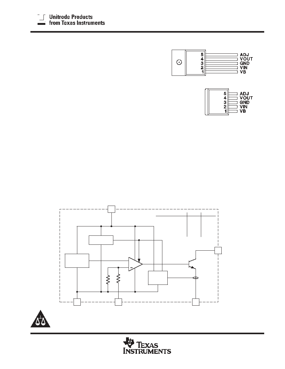
block diagram
+
THERMAL
SHUTDOWN
1.2 V
BANDGAP
REFERENCE
R2
R1
3
5
SHORT
CIRCUIT
SENSE
2
1
4
UC382-ADJ
UC382-1 (1.5 V)
UC382-2 (2.1 V)
UC382-3 (2.5 V)
OPEN
0
2 k
500
2 k
1.5 k
2 k
2.16 k
R1
R2
ADJ
GND
VOUT
VIN
VB
UDG-00080
Copyright
2000-2004, Texas Instruments Incorporated
PRODUCTION DATA information is current as of publication date.
Products conform to specifications per the terms of Texas Instruments
standard warranty. Production processing does not necessarily include
testing of all parameters.
Please be aware that an important notice concerning availability, standard warranty, and use in critical applications of
Texas Instruments semiconductor products and disclaimers thereto appears at the end of this data sheet.
5-PIN TO-263
TD PACKAGE
(TOP VIEW)
5-PIN TO-220
T PACKAGE (TOP VIEW)
Note: Tab = Ground
All trademarks are the property of their respective owners.
UC282 1, UC282 2, UC282 3, UC282 ADJ, UC382 1, UC382 2, UC382 3, UC382 ADJ
FAST LDO LINEAR REGULATOR
SLUS317B - JANUARY 2000 - REVISED FEBRUARY 2004
2
POST OFFICE BOX 655303
∑
DALLAS, TEXAS 75265
absolute maximum ratings over operating free-air temperature (unless otherwise noted)
}
VB
13 V
. . . . . . . . . . . . . . . . . . . . . . . . . . . . . . . . . . . . . . . . . . . . . . . . . . . . . . . . . . . . . . . . . . . . . . . . . . . . . . . . . . . . . . .
VIN
7.5 V
. . . . . . . . . . . . . . . . . . . . . . . . . . . . . . . . . . . . . . . . . . . . . . . . . . . . . . . . . . . . . . . . . . . . . . . . . . . . . . . . . . . . .
Output voltage
1.2 V to 6.0 V
. . . . . . . . . . . . . . . . . . . . . . . . . . . . . . . . . . . . . . . . . . . . . . . . . . . . . . . . . . . . . . . . . . . . .
Storage temperature, T
stg
-65
∞
C to 150
∞
C
. . . . . . . . . . . . . . . . . . . . . . . . . . . . . . . . . . . . . . . . . . . . . . . . . . . . . . . . .
Junction temperature, T
J
-55
∞
C to 150
∞
C
. . . . . . . . . . . . . . . . . . . . . . . . . . . . . . . . . . . . . . . . . . . . . . . . . . . . . . . . . .
Lead temperature (soldering, 10 seconds)
300
∞
C
. . . . . . . . . . . . . . . . . . . . . . . . . . . . . . . . . . . . . . . . . . . . . . . . . .
Stresses beyond those listed under "absolute maximum ratings" may cause permanent damage to the device. These are stress ratings only, and
functional operation of the device at these or any other conditions beyond those indicated under "recommended operating conditions" is not
implied. Exposure to absolute-maximum-rated conditions for extended periods may affect device reliability.
}
Currents are positive into, negative out of the specified terminal. Consult Packaging Section of Databook for thermal limitations and
considerations of packages.
AVAILABLE OPTIONS(1)
PACKAGED DEVICES
TJ
TO-220 (T)
TO-263 (TD)(2)
TJ
OUTPUT VOLTAGE
OUTPUT VOLTAGE
1.5 V
2.1 V
2.5 V
1.2 V or ADJ
1.5 V
2.1 V
2.5 V
1.2 V or ADJ
≠40
∞
C to 100
∞
C
282T-1
282T-2
282T-3
282T-ADJ
282TD-1
282TD-2
282TD-3
282TD-ADJ
0
∞
C to 100
∞
C
382T-1
382T-2
382T-3
382T-ADJ
382TD-1
382TD-2
382TD-3
382TD-ADJ
1. For more package and ordering information, see the Package Option Addendum located at the end of this data sheet.
2. For 50 piece reel, add KTTT (e.g., UC282TDKTTT-1); for 500 piece reel, add TR (e.g., UC282TDTR-1).
electrical characteristics, T
A
= -40
∞
C to 100
∞
C for the UC282-X series and 0
∞
C to 100
∞
C for the
UC382-X, VB = 5 V, VIN = 3.3 V, VOUT = 2.5 V for the UC382-ADJ, T
A
= T
J
, (unless otherwise stated)
UC382-3 fixed 2.5 V, 3-A family
PARAMETERS
TEST CONDITIONS
MIN
TYP
MAX
UNITS
Output voltage (IVOUT = 100 mA)
UC382-3
2.475
2.500
2.525
V
Output voltage (IVOUT = 100 mA)
UC282-3
2.450
2.500
2.525
V
Load regulation
IVOUT = 10 mA to 3 A
0.5
4
mV
VIN PSSR
80
100
dB
VB PSSR
50
60
dB
IVOUT = 3 A,
TJ = 25
∞
C
350
425
mV
VIN dropout voltage = VIN-VOUT
IVOUT = 3 A,
UC382-3
350
450
mV
VIN dropout voltage = VIN-VOUT
IVOUT = 3 A,
UC282-3
350
500
mV
VB dropout = VB-VOUT
IVOUT = 3 A,
UC382-3
1.8
2.10
V
VB dropout = VB-VOUT
IVOUT = 3 A,
UC282-3
1.8
2.20
V
Short circuit current limit
3.3
4.5
A
VB current
IVOUT = 10 mA
6
11
mA
VB current
IVOUT = 3 A
18
60
mA
VIN current
IVOUT = 3 A
2.94
2.97
A
UC282 1, UC282 2, UC282 3, UC282 ADJ, UC382 1, UC382 2, UC382 3, UC382 ADJ
FAST LDO LINEAR REGULATOR
SLUS317B - JANUARY 2000 - REVISED FEBRUARY 2004
3
POST OFFICE BOX 655303
∑
DALLAS, TEXAS 75265
electrical characteristics, T
A
= -40
∞
C to 100
∞
C for the UC282-X series and 0
∞
C to 100
∞
C for the
UC382-X, VB = 5 V, VIN = 3.3 V, VOUT = 2.5 V for the UC382-ADJ, T
A
= T
J
, (unless otherwise stated)
UC382-2 fixed 2.1 V, 3-A family
PARAMETERS
TEST CONDITIONS
MIN
TYP
MAX
UNITS
Output voltage (IVOUT = 100 mA)
UC382-2
2.079
2.100
2.121
V
Output voltage (IVOUT = 100 mA)
UC282-2
2.058
2.100
2.121
V
Load regulation
IVOUT = 10 mA to 3 A
0.5
4
mV
VIN PSSR
80
100
dB
VB PSSR
52
62
dB
IVOUT = 3 A,
TJ = 25
∞
C
350
425
mV
VIN dropout voltage = VIN-VOUT
IVOUT = 3 A,
UC382-2
350
450
mV
VIN dropout voltage = VIN-VOUT
IVOUT = 3 A,
UC282-2
350
500
mV
VB dropout = VB-VOUT
IVOUT = 3 A,
UC382-2
1.8
2.10
V
VB dropout = VB-VOUT
IVOUT = 3 A,
UC282-2
1.8
2.20
V
Short circuit current limit
3.3
4.5
A
VB current
IVOUT = 10 mA
6
11
mA
VB current
IVOUT = 3 A
18
60
mA
VIN current
IVOUT = 3 A
2.94
2.97
A
UC382-1 fixed 1.5 V, 3-A family
PARAMETERS
TEST CONDITIONS
MIN
TYP
MAX
UNITS
Output voltage (IVOUT = 100 mA)
UC382-1
1.485
1.500
1.515
V
Output voltage (IVOUT = 100 mA)
UC282-1
1.470
1.500
1.515
V
Load regulation
IVOUT = 10 mA to 3 A
0.5
4
mV
VIN PSSR
80
100
dB
VB PSSR
55
65
dB
IVOUT = 3 A,
TJ = 25
∞
C
350
425
mV
VIN dropout voltage = VIN-VOUT
IVOUT = 3 A,
UC382-1
350
450
mV
VIN dropout voltage = VIN-VOUT
IVOUT = 3 A,
UC282-1
350
500
mV
VB dropout = VB-VOUT
IVOUT = 3 A,
UC382-1
1.8
2.10
V
VB dropout = VB-VOUT
IVOUT = 3 A,
UC282-1
1.8
2.20
V
Short circuit current limit
3.3
4.5
A
VB current
IVOUT = 10 mA
6
11
mA
VB current
IVOUT = 3 A
18
60
mA
VIN current
IVOUT = 3 A
2.94
2.97
A
UC282 1, UC282 2, UC282 3, UC282 ADJ, UC382 1, UC382 2, UC382 3, UC382 ADJ
FAST LDO LINEAR REGULATOR
SLUS317B - JANUARY 2000 - REVISED FEBRUARY 2004
4
POST OFFICE BOX 655303
∑
DALLAS, TEXAS 75265
electrical characteristics, T
A
= -40
∞
C to 100
∞
C for the UC282-X series and 0
∞
C to 100
∞
C for the
UC382-X, VB = 5 V, VIN = 3.3 V, VOUT = 2.5 V for the UC382-ADJ, T
A
= T
J
, (unless otherwise stated)
UC382-ADJ adjustable, 3-A family
PARAMETERS
TEST CONDITIONS
MIN
TYP
MAX
UNITS
ADJ voltage (IVOUT = 100 mA)
UC382-ADJ
1.188
1.200
1.212
V
ADJ voltage (IVOUT = 100 mA)
UC282-ADJ
1.176
1.200
1.212
V
Load regulation
IVOUT = 10 mA to 3 A
0.5
4
mV
VIN PSSR
VOUT programmed for 2.5 V
80
100
dB
VB PSSR
VOUT programmed for 2.5 V
50
60
dB
IVOUT = 3 A,
TJ = 25
∞
C
350
425
mV
VIN dropout voltage = VIN-VOUT
IVOUT = 3 A,
UC382-ADJ
350
450
mV
VIN dropout voltage = VIN-VOUT
IVOUT = 3 A,
UC282-ADJ
350
500
mV
VB dropout = VB-VOUT
IVOUT = 3 A,
UC382-ADJ
1.8
2.10
V
VB dropout = VB-VOUT
IVOUT = 3 A,
UC282-ADJ
1.8
2.20
V
Short circuit current limit
3.3
4.5
A
VB current
IVOUT = 10 mA
6
11
mA
VB current
IVOUT = 3 A
18
60
mA
VIN current
IVOUT = 3 A
2.94
2.97
A
pin descriptions
ADJ: In the adjustable version, the user programs the output voltage with two external resistors. The resistors
should be 0.1% for high accuracy. The output amplifier is configured as a non-inverting-operational amplifier.
The resistors should meet the criteria of R3 || R4 < 100
. Connect ADJ to VOUT for an output voltage of 1.2 V.
Note that the point at which the feedback network is connected to the output is the Kelvin sense point. For -1,
-2, and -3 versions, ADJ pin is tied to VOUT to obtain specified output voltage.
GND: For accurate results, the GND pin should be referenced to the load ground.
VB: Supplies power to all circuits of the regulator except the collector of the output-power transistor. The 2-V
headroom from VB to VOUT allows the use of a Darlington output stage for inherently-low-output impedance
and fast response. (Dropout is derated for junction temperatures below 0
∞
C.)
VIN: Supplies the current to the collector of the output-power transistor only. The dropout (VIN-VOUT) is under
100 mV for light loads; maximum dropout is 450 mV at 3 A for T
J
= 0
∞
C to 100
∞
C. (Dropout is derated for junction
temperatures over 100
∞
C.) At full load, the majority of the VB current is going to the load.
VOUT: This pin should be connected to the load via a low impedance path. Avoid connectors which add
significant inductance and resistance. Note that even though a Kelvin sense is available through a 5-pin
package, care must be taken since voltage drops along wire traces add to the dropout voltage.
UC282 1, UC282 2, UC282 3, UC282 ADJ, UC382 1, UC382 2, UC382 3, UC382 ADJ
FAST LDO LINEAR REGULATOR
SLUS317B - JANUARY 2000 - REVISED FEBRUARY 2004
5
POST OFFICE BOX 655303
∑
DALLAS, TEXAS 75265
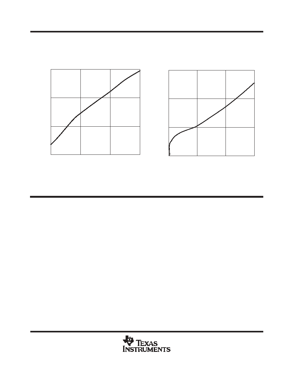
pin descriptions (continued)
Figure 1
DROPOUT VOLTAGE (V
B
- V
OUT
)
vs
LOAD CURRENT
3
IL- Load Current - A
2
1
0
1.7
1.8
1.9
1.6
V
DO
- Dropout V
oltage - V
TJ = 27
5
C
Figure 2
DROPOUT VOLTAGE (V
IN
- V
OUT
)
vs
LOAD CURRENT
3 A
2 A
1 A
100 mA
100
200
300
400
IL - Load Current - A
V
DO
- Dropout V
oltage - mV
TJ = 27
5
C
APPLICATION INFORMATION
The UC382 is easy to use. The adjustable version requires two 0.1% resistors to set the output voltage. The
fixed versions of the UC382 require no external resistors. All versions of the UC382 require decoupling
capacitors on the input and output. In a typical application, VB and VIN are driven from switching power supplies
which may have large filter capacitors at their outputs. If the UC382 is further than 12 inches from the power
supply, it is recommended to add local decoupling as close as possible to the linear regulator.
Decouple the output of the UC382 with at least 100
µ
F of high-quality tantalum or Sanyo OSCON capacitors
close to the VOUT pin for maximum stability. Many applications involving Ultra-Fast GTL or BTL applications
require additional capacitance close to the load. The exact amount will vary according to speed and magnitude
of the load transients and the tolerance allowed for transients on VOUT. When specifying the decoupling
capacitors, the series resistance of the capacitor bank is an important factor in its ability to filter load transients.
The UC382 allows for Kelvin sensing the voltage at the load. This improves regulation performance and
eliminates the voltage drops due to wire-trace resistance. This voltage drop must be added to the headroom
(VIN to VOUT and VB to VOUT). The dropout of 450 mV is measured at the pins and does not include additional
drops due to trace resistance. The minimum load current is 10 mA.
Two or more UC382's may be used in parallel. While stable, this arrangement does degrade the transient
response.