Document Outline
- Application Notes
- Design Notes
SLUS387A - JUNE 19
94
- REVISED - MAY 2003
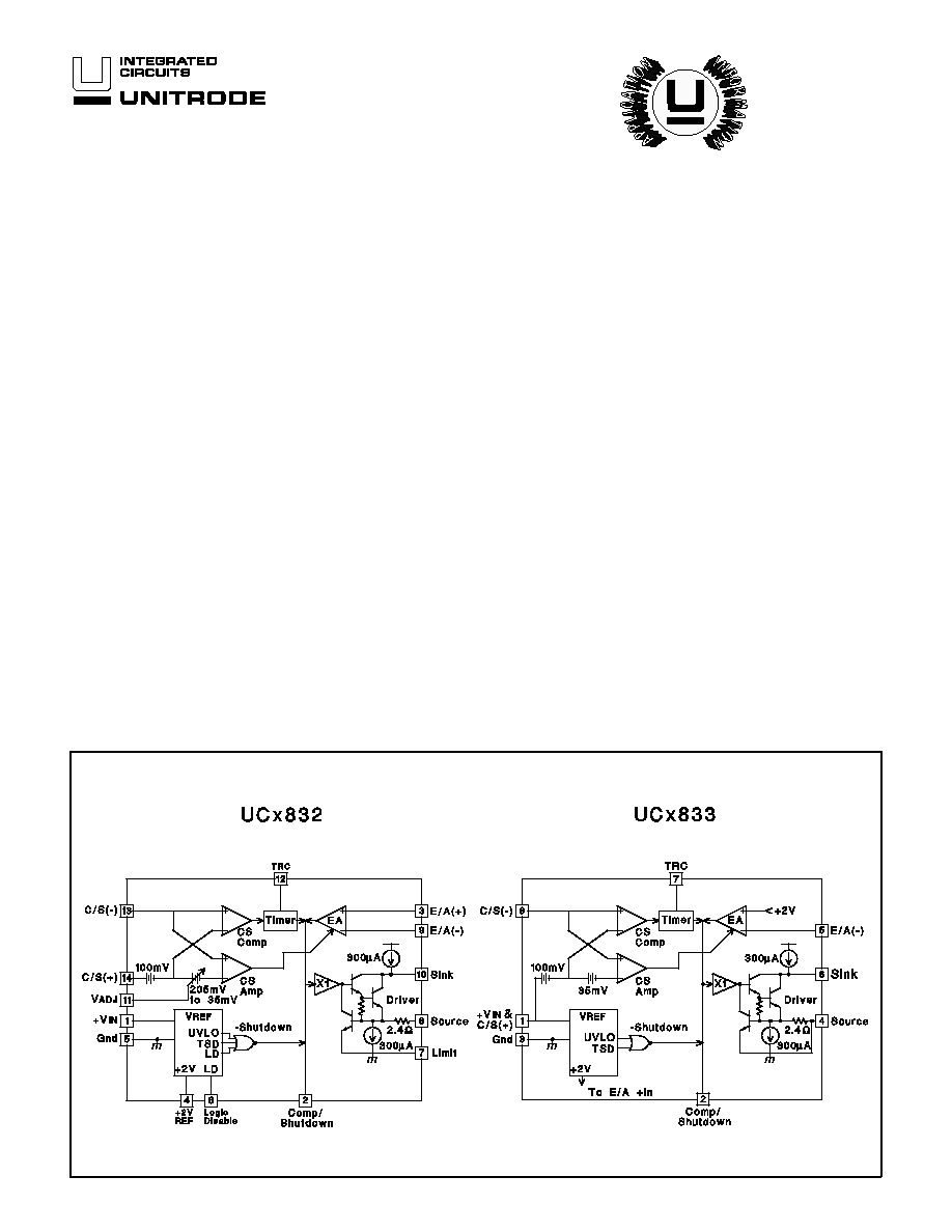
BLOCK DIAGRAMS
∑
Precision 1% Reference
∑
Over-Current Sense Threshold
Accurate to 5%
∑
Programmable Duty-Ratio
Over-Current Protection
∑
4.5
V to 36
V Operation
∑
100mA Output Drive, Source
,
or
Sink
∑
Under-Voltage Lockout
Additional Features of the UC
2
832
series:
∑
Adjustable Current Limit to
Current Sense Ratio
∑
Separate +V
IN
terminal
∑
Programmable Driver Current
Limit
∑
Access to V
REF
and E/A(+)
∑
Logic-Level Disable Input
The UC
2
832 and UC
3
833 series of precision linear regulators include all the
control functions required in the design of very low dropout linear regulators.
Additionally, they feature an innovative duty-ratio current limiting technique
which provides peak load capability while limiting the average power dissipa-
tion of the external pass transistor during fault conditions. When the load cur-
rent reaches an accurately programmed threshold, a gated-astable timer is
enabled, which switches the regulator's pass device off and on at an externally
programmable duty-ratio. During the on-time of the pass element, the output
current is limited to a value slightly higher than the trip threshold of the duty-ra-
tio timer. The constant-current-limit is programmable on the UCx832 to allow
higher peak current during the on-time of the pass device. With duty-ratio con-
trol, high initial load demands and short circuit protection may both be accom-
modated without extra heat sinking or foldback current limiting. Additionally, if
the timer pin is grounded, the duty-ratio timer is disabled, and the IC operates
in constant-voltage/constant-current regulating mode.
These IC's include a 2 Volt (
±
1%) reference, error amplifier, UVLO, and a high
current driver that has both source and sink outputs, allowing the use of either
NPN or PNP external pass transistors. Safe operation is assured by the inclu-
sion of under-voltage lockout (UVLO) and thermal shutdown.
The UC
3
833 family includes the basic functions of this design in a low-cost, 8-
pin mini-dip package, while the UC
2
832 series provides added versatility with
the availability of 14 pins. Packaging options include plastic (N suffix), or ce-
ramic (J suffix). Specified operating temperature ranges are: commercial (0∞C
to 70∞C), order UC3832/3 (N or J);
and
industrial (≠
40
∞C to 85∞C), order
UC2832/3
(N or J)
.
Surface mount
packaging is also available.
UC1832
UC2832/3
UC3832/3
Precision Low Dropout Linear Controllers
FEATURES
DESCRIPTION
UDG-92040
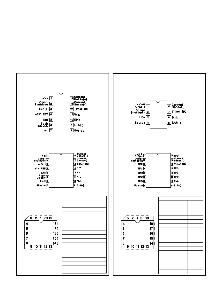
CONNECTION DIAGRAMS
DIL-14 (Top View)
J Or N Package
SOIC-16 (Top View)
DW Package
UC1832
UC2832/3
UC3832/3
PACKAGE PIN FUNCTION
FUNCTION
PIN
N/C
1
+V
IN
2
Comp/Shutdown
3
E/A(+)
4
+2V REF
5
N/C
6
Gnd
7
Logic Disable
8
Limit
9
Source
10
N/C
11
E/A(-)
12
Sink
13
V
ADJ
14
N/C
15-17
Timer RC
18
Current Sense(-)
19
Current Sense(+)
20
LCC-20 & PLCC-20
L & Q Package
(Top View)
ABSOLUTE MAXIMUM RATINGS
Supply Voltage +V
IN
. . . . . . . . . . . . . . . . . . . . . . . . . . . . . . . 40V
Driver Output Current (Sink or Source) . . . . . . . . . . . . . 450mA
Driver Sink to Source Voltage . . . . . . . . . . . . . . . . . . . . . . . 40V
TRC Pin Voltage. . . . . . . . . . . . . . . . . . . . . . . . . . ≠0.3V to 3.2V
Other Input Voltages. . . . . . . . . . . . . . . . . . . . . . . ≠0.3V to +V
IN
Operating Junction Temperature (note 2) . . . ≠55∞C to +150∞C
Storage Temperature . . . . . . . . . . . . . . . . . . . ≠65∞C to +150∞C
Lead Temperature (Soldering, 10 Seconds) . . . . . . . . . . 300
∞
C
Note 1: Unless otherwise indicated, voltages are referenced to
ground and currents are positive into, negative out of, the speci-
fied terminals.
Note 2: See Unitrode Integrated Circuits databook for
information regarding thermal specifications and limitations of
packages.
UC
2
832
UC
3
833
PACKAGE PIN FUNCTION
FUNCTION
PIN
+V
IN
& C/S(+)
1
N/C
2
N/C
3
N/C
4
Comp/Shutdown
5
Gnd
6
N/C
7
N/C
8
N/C
9
Source
10
N/C
11
E/A(-)
12
N/C
13
N/C
14
Sink
15
Timer RC
16
Current Sense(+)
17
N/C
18-20
SOIC-16 (Top View)
DW Package
DIL-8 (Top View)
J Or N Package
LCC-20 & PLCC-20
L & Q Package
(Top View)
2
PARAMETER
TEST CONDITIONS
MIN
TYP
MAX
UNITS
Input Supply
Supply Current
+V
IN
= 6
V
6.5
10
mA
+V
IN
= 36
V
9.5
15
mA
Logic Disable = 2
V (UCx832 only)
3.3
mA
Reference Section
Output Voltage (Note 3)
T
J
= 25
∞
C, I
DRIVER
= 10
mA
1.98
2.00
2.02
V
over temperature, I
DRIVER
= 10
mA
1.96
2.00
2.04
V
Load Regulation (UCx832 only)
I
O
= 0 to 10
m
-10
-5.0
mV
Line Regulation
+V
IN
= 4.5
V
to 36
V, I
DRIVER
= 10
m
0.033
0.5
mV/V
Under-Voltage Lockout Threshold
3.6
4.5
V
Logic Disable Input (UCx832 only)
Threshold Voltage
1.3
1.4
1.5
V
Input Bias Current
Logic Disable = 0
V
-5.0
-1.0
µ
A
Current Sense Section
Comparator Offset
95
100
105
mV
Over Temperature
93
100
107
mV
Amplifier Offset (UCx833 only)
110
135
170
mV
Amplifier Offset (UCx832 only)
V
ADJ
= Open
110
135
170
mV
V
ADJ
= 1
V
180
235
290
mV
V
ADJ
= 0
V
250
305
360
mV
Input Bias Current
V
CM
= +V
IN
65
100
135
µ
A
Input Offset Current (UCx832 only)
V
CM
= +V
IN
-10
10
µ
A
Amplifier CMRR (UCx832 only)
V
CM
= 4.1
V to +
V
IN
+
0.3
80
dB
Transconductance
I
COMP
=
±
100
µ
A
65
mS
V
ADJ
Input Current (UCx832 only)
V
ADJ
= 0V
-10
-1
µ
A
Timer
Inactive Leakage Current
C/S(+) = C/S(-) = +V
IN
; TRC pin = 2
V
0.25
1.0
µ
A
Active Pullup Current
C/S(+) = +V
IN
, C/S(-) = +V
IN
- 0.4V; TRC pin = 0
V
-345
-270
-175
µ
A
Duty Ratio (note 4)
ontime/period, R
T
= 200k, C
T
= 0.27
µ
F
4.8
%
Period (notes 4,5)
ontime + offtime, R
T
= 200k, C
T
= 0.27
µ
F
36 ms
Upper Trip Threshold (Vu)
1.8
V
Lower Trip Threshold (Vl)
0.9
V
Trip Threshold Ratio
Vu/Vl
2.0
V/V
Error Amplifier
Input Offset Voltage (UCx832 only)
V
CM
= V
COMP
= 2
V
-8.0
8.0
mV
Input Bias Current
V
CM
= V
COMP
= 2
V
-4.5
-1.1
µ
A
Input Offset Current (UCx832 only)
V
CM
= V
COMP
= 2
V
-1.5
1.5
µ
A
AVOL
V
COMP
= 1
V to 13
V
50
70
dB
CMRR (UCx832 only)
V
CM
= 0V to +V
IN
- 3
V
60
80
dB
PSRR (UCx832 only)
V
CM
= 2
V, +V
IN
= 4.5
V
to 36
90
dB
Transconductance
I
COMP
=
±
10
µ
A
4.3
mS
VOH
I
COMP
= 0, Volts below +V
IN
.95
1.3
V
VOL
I
COMP
= 0
.45
0.7
V
IOH
V
COMP
= 2
V
-700
-500
-100
µ
A
UC1832
UC2832/3
UC3832/3
Unless otherwise stated, specifications hold for
TA = 0∞C to 70∞C for the
UC3832/3, ≠
40
∞C to 85∞C
for the UC2832/3,
+V
IN
= 15V, Driver sink = +V
IN
, C/S(+) voltage = +V
IN.
T
A
=T
J
.
ELECTRICAL CHARACTERISTICS:
3
Unless otherwise stated, specifications hold for TA = 0∞C to 70∞C for the UC3832/3, ≠40∞C to
85∞C for the UC2832/3, +VIN = 15 V, Driver sink =
+V
IN
, C/S(+) voltage = +V
IN
. T
A
=T
J
.
ELECTRICAL
CHARACTERISTICS (cont.)
UC1832
UC2832/3
UC3832/3
PARAMETER
TEST CONDITIONS
MIN
TYP
MAX
UNITS
Error Amplifier (cont.)
IOL
V
COMP
= 2
V, C/S(-) = +V
IN
100
500
700
µ
A
V
COMP
= 2
V, C/S(-) = +V
IN
- 0.4
V
2
6
mA
Driver
Maximum Current
Driver Limit & Source pins common; T
J
= 25∞C
200
300
400
mA
Over Temperature
100
300
450
mA
Limiting Voltage (UCx832 only)
Driver Limit to Source voltage at current limit,
I
SOURCE
= -10
mA; T
J
= 25∞C (Note 6)
.72
V
Internal Current Sense Resistance
T
J
= 25∞C (Note 6)
2.4
Pull-Up Current at Driver Sink
Compensation/Shutdown = 0.4
V; Driver Sink = +V
IN
- 1V
-800
-300
-100
µ
A
Compensation/Shutdown = 0.4
V, +V
IN
= 36
V; Driver
Sink = 35
V
-1000
-300
-75
µ
A
Pull-Down Current at Driver Source
Compensation/Shutdown = 0.4
V; Driver Source = 1
V
150
300
700
µ
A
Saturation Voltage Sink to Source
Driver Source = 0
V; Driver Current = 100
mA
1.5
V
Maximum Source Voltage
Driver Sink = +V
IN
, Driver Current = 100
mA
Volts below +
V
IN
3.0
V
UVLO Sink Leakage
+V
IN
= C/S(+) = C/S(-) = 2.5
V, Driver Sink = 15
V, Driver
Source = 0
V, TA = 25∞C
25
µ
A
Maximum Reverse Source Voltage
Compensation/Shutdown = 0
V; I
SOURCE
= 100
µ
A,
+V
IN
= 3
V
1.6
V
Thermal Shutdown
160
∞C
Note 3: On the UCx833 this voltage is defined as the regulating level at the error amplifier inverting input, with the error amplifier
driving V
SOURCE
to 2
V.
Note 4: These parameters are first-order supply-independent, however both may vary with supply for +V
IN
less than about 4
V. This
supply variation will cause a slight change in the timer period and duty cycle, although a high off-time/on-time ratio will be main-
tained.
Note 5: With recommended R
T
value of 200k, T
OFF
R
T
C
T
* ln(Vu/Vl)
±
10%.
Note 6: The internal current limiting voltage has a temperature dependence of approximately -2.0
mV/∞C, or -2800
ppm/∞C. The inter-
nal 2.4
sense resistor has a temperature dependance of approximately +1500
ppm/∞C.
UDG-92041-1
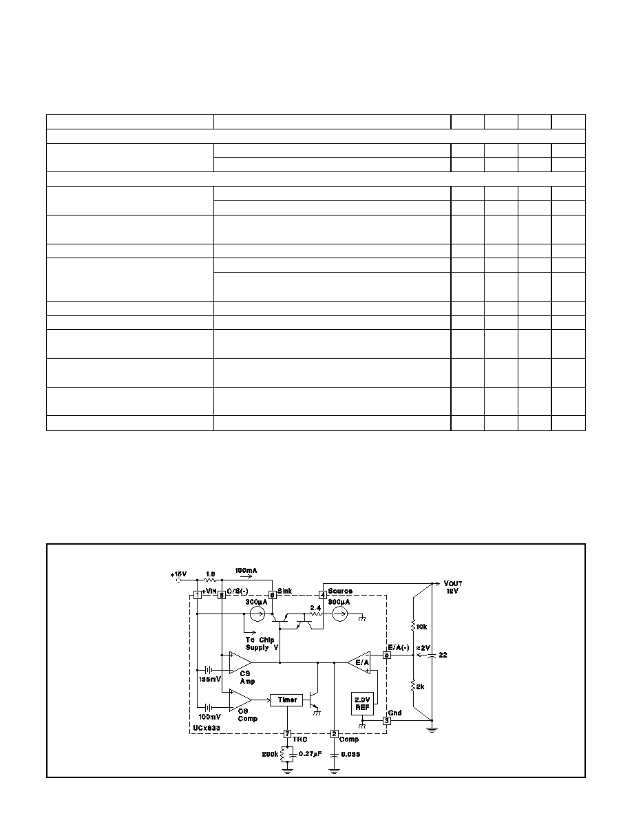
APPLICATION AND OPERATION INFORMATION
NPN Pass (Local 100mA Regulator) (UCx833)
4

UC1832
UC2832/3
UC3832/3
APPLICATION AND OPERATION INFORMATION (cont.)
UDG-92042-1
UDG-92043-1
PNP Pass (Low Drop-Out Regulator) (UCx833)
NPN Pass (Medium Power, Low Drop-Out Regulator) (UCx832)
For any power supply, the rate at which the total output
capacitance can be charged depends on the maximum
output current available and on the nature of the load. For
a constant-current current-limited power supply, the out-
put will come up if the load asks for less than the maxi-
mum available short-circuit limit current.
To guarantee recovery of a duty-ratio current-limited
power supply from a short-circuited load condition, there
is a maximum total output capacitance which can be
charged for a given unit ON time. The design value of ON
time can be adjusted by changing the timing capacitor.
Nominally, T
ON
= 0.693 x 10k x C
T
.
Typically, the IC regulates output current to a maximum of
I
MAX
= K x I
TH
, where I
TH
is the timer trip-point current,
and
K
=
Current Sense Amplifier
Offset Voltage
100
mA
1.35 for UCx833, and is variable from 1.35 to 3.05
with V
ADJ
for the UCx832.
For a worst-case constant-current load of value just less
than I
TH
, C
MAX
can be estimated from:
C
MAX
=
((
K
-
1
)
I
TH
)
(
T
ON
V
OUT
)
,
where V
OUT
is the nominal regulator output voltage.
For a resistive load of value R
L
, the value of C
MAX
can be
estimated from:
C
MAX
=
T
ON
R
L
∑
1
In
[
(
1
-
V
OUT
K
∑
I
TH
∑
R
L
)
-
1
]
.
Estimating Maximum Load Capacitance
5
UC1832
UC2832/3
UC3832/3
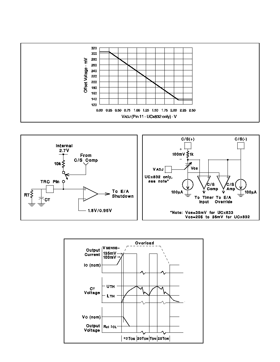
Current Sense Amplifier Offset Voltage vs V
ADJ
UCx832/33 Timer Function
UCx832/33 Current Sense Input Configuration
APPLICATION AND OPERATION INFORMATION (cont.)
Load current, timing capacitor voltage, and output voltage of
the regulator under fault conditions.
6
UC1832
UC2832/3
UC3832/3
UNITRODE CORPORATION
7 CONTINENTAL BLVD.
∑
MERRIMACK, NH 03054
TEL. (603) 424-2410
∑
FAX (603) 424-3460
APPLICATION AND OPERATION INFORMATION (cont.)
7

IMPORTANT NOTICE
Texas Instruments and its subsidiaries (TI) reserve the right to make changes to their products or to discontinue
any product or service without notice, and advise customers to obtain the latest version of relevant information
to verify, before placing orders, that information being relied on is current and complete. All products are sold
subject to the terms and conditions of sale supplied at the time of order acknowledgement, including those
pertaining to warranty, patent infringement, and limitation of liability.
TI warrants performance of its semiconductor products to the specifications applicable at the time of sale in
accordance with TI's standard warranty. Testing and other quality control techniques are utilized to the extent
TI deems necessary to support this warranty. Specific testing of all parameters of each device is not necessarily
performed, except those mandated by government requirements.
CERTAIN APPLICATIONS USING SEMICONDUCTOR PRODUCTS MAY INVOLVE POTENTIAL RISKS OF
DEATH, PERSONAL INJURY, OR SEVERE PROPERTY OR ENVIRONMENTAL DAMAGE ("CRITICAL
APPLICATIONS"). TI SEMICONDUCTOR PRODUCTS ARE NOT DESIGNED, AUTHORIZED, OR
WARRANTED TO BE SUITABLE FOR USE IN LIFE-SUPPORT DEVICES OR SYSTEMS OR OTHER
CRITICAL APPLICATIONS. INCLUSION OF TI PRODUCTS IN SUCH APPLICATIONS IS UNDERSTOOD TO
BE FULLY AT THE CUSTOMER'S RISK.
In order to minimize risks associated with the customer's applications, adequate design and operating
safeguards must be provided by the customer to minimize inherent or procedural hazards.
TI assumes no liability for applications assistance or customer product design. TI does not warrant or represent
that any license, either express or implied, is granted under any patent right, copyright, mask work right, or other
intellectual property right of TI covering or relating to any combination, machine, or process in which such
semiconductor products or services might be or are used. TI's publication of information regarding any third
party's products or services does not constitute TI's approval, warranty or endorsement thereof.
Copyright
©
2003
, Texas Instruments Incorporated