
UC2832-EP
PRECISION LOW DROPOUT LINEAR CONTROLLER
SGLS147A ≠ JANUARY 2003 ≠ REVISED MARCH 2003
1
POST OFFICE BOX 655303
∑
DALLAS, TEXAS 75265
D
Controlled Baseline
≠ One Assembly/Test Site, One Fabrication
Site
D
Extended Temperature Performance of
≠40
∞
C to 105
∞
C
D
Enhanced Diminishing Manufacturing
Sources (DMS) Support
D
Enhanced Product Change Notification
D
Qualification Pedigree
D
Precision 1% Reference
D
Over-Current Sense Threshold Accurate to
5%
D
Programmable Duty-Ratio Over-Current
Protection
Component qualification in accordance with JEDEC and industry
standards to ensure reliable operation over an extended
temperature range. This includes, but is not limited to, Highly
Accelerated Stress Test (HAST) or biased 85/85, temperature
cycle, autoclave or unbiased HAST, electromigration, bond
intermetallic life, and mold compound life. Such qualification
testing should not be viewed as justifying use of this component
beyond specified performance and environmental limits.
D
4.5 V to 36 V Operation
D
100 mA Output Drive, Source or Sink
D
Under-Voltage Lockout
D
Adjustable Current Limit to Current Sense
Ratio
D
Separate +V
IN
terminal
D
Programmable Driver Current Limit
D
Access to VREF and E/A(+)
D
Logic-Level Disable Input
description
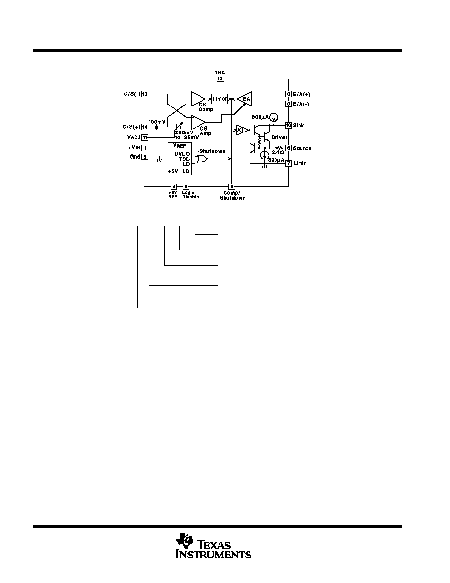
The UC2832 series of precision linear regulators include all the control functions required in the design of very
low dropout linear regulators. Additionally, they feature an innovative duty-ratio current limiting technique which
provides peak load capability while limiting the average power dissipation of the external pass transistor during
fault conditions. When the load current reaches an accurately programmed threshold, a gated-astable timer is
enabled, which switches the regulator's pass device off and on at an externally programmable duty-ratio. During
the on-time of the pass element, the output current is limited to a value slightly higher than the trip threshold
of the duty-ratio timer. The constant-current-limit is programmable on the UC2832 to allow higher peak current
during the on-time of the pass device. With duty-ratio control, high initial load demands and short circuit
protection may both be accommodated without extra heat sinking or foldback current limiting. Additionally, if the
timer pin is grounded, the duty-ratio timer is disabled, and the IC operates in constant-voltage/constant-current
regulating mode.
These IC's include a 2 Volt (
±
1%) reference, error amplifier, UVLO, and a high current driver that has both source
and sink outputs, allowing the use of either NPN or PNP external pass transistors. Safe operation is assured
by the inclusion of under-voltage lockout (UVLO) and thermal shutdown.
ORDERING INFORMATION
TA
PACKAGEß
ORDERABLE
PART NUMBER
TOP-SIDE
MARKING
≠40
∞
C to 105
∞
C
SOP ≠ DW
Tape and reel
UC2832TDWREP
UC2832TEP
≠40
∞
C to 105
∞
C
SOP ≠ DW
Tube
UC2832TDWEP
UC2832TEP
Package drawings, standard packing quantities, thermal data, symbolization, and PCB design
guidelines are available at www.ti.com/sc/package.
Copyright
2003, Texas Instruments Incorporated
PRODUCTION DATA information is current as of publication date.
Products conform to specifications per the terms of Texas Instruments
standard warranty. Production processing does not necessarily include
testing of all parameters.
Please be aware that an important notice concerning availability, standard warranty, and use in critical applications of
Texas Instruments semiconductor products and disclaimers thereto appears at the end of this data sheet.
DW PACKAGE
(TOP VIEW)
1
2
3
4
5
6
7
8
16
15
14
13
12
11
10
9
+V
IN
Comp/Shutdown
E/A(+)
+2V REF
GND
Logic Disable
Limit
Source
Current Sense(+)
Current Sense(≠)
Timer RC
NC
V
ADJ
NC
Sink
E/A(≠)
NC = No Connect
UC2832-EP
PRECISION LOW DROPOUT LINEAR CONTROLLER
SGLS147A ≠ JANUARY 2003 ≠ REVISED MARCH 2003
2
POST OFFICE BOX 655303
∑
DALLAS, TEXAS 75265
block diagram
Ordering Information
UC
2
PACKAGE
DW = Plastic SOIC
PRODUCT OPTION
DW
TAPE and REEL INDICATOR
R
283
EP
ENHANCED PLASTIC INDICATOR
T
TEMPERATURE INDICATOR
T = ≠40
_
C to 105
_
C

UC2832-EP
PRECISION LOW DROPOUT LINEAR CONTROLLER
SGLS147A ≠ JANUARY 2003 ≠ REVISED MARCH 2003
3
POST OFFICE BOX 655303
∑
DALLAS, TEXAS 75265
absolute maximum ratings over operating free-air temperature range (unless otherwise noted)
V
IN
supply voltage
40 V
. . . . . . . . . . . . . . . . . . . . . . . . . . . . . . . . . . . . . . . . . . . . . . . . . . . . . . . . . . . . . . . . . . . . . . . . .
Driver output current (sink or source), I
O
450
mA
. . . . . . . . . . . . . . . . . . . . . . . . . . . . . . . . . . . . . . . . . . . . . . . . . .
Driver sink to source voltage
40 V
. . . . . . . . . . . . . . . . . . . . . . . . . . . . . . . . . . . . . . . . . . . . . . . . . . . . . . . . . . . . . . . .
TRC pin voltage
≠0.3 V to 3.2 V
. . . . . . . . . . . . . . . . . . . . . . . . . . . . . . . . . . . . . . . . . . . . . . . . . . . . . . . . . . . . . . . . . .
Other input voltages
≠0.3 V to supply voltage
. . . . . . . . . . . . . . . . . . . . . . . . . . . . . . . . . . . . . . . . . . . . . . . . . . . . . . .
Operating jucntion temperature range, T
J
≠55
_
C to 150
_
C
. . . . . . . . . . . . . . . . . . . . . . . . . . . . . . . . . . . . . . . . . . . .
Storage temperature range, T
stg
≠65
_
C to 150
_
C
. . . . . . . . . . . . . . . . . . . . . . . . . . . . . . . . . . . . . . . . . . . . . . . . . . . .
Lead temperature soldering 1,6 mm (1/16 inch) from case for 10 seconds
300
_
C
. . . . . . . . . . . . . . . . . . . . . . .
Stresses beyond those listed under "absolute maximum ratings" may cause permanent damage to the device. These are stress ratings only, and
functional operation of the device at these or any other conditions beyond those indicated under "recommended operating conditions" is not
implied. Exposure to absolute-maximum-rated conditions for extended periods may affect device reliability.
Unless otherwise indicated, voltages are reference to ground and currents are positive into and negative out of the specified terminals.
electrical characteristics, T
A
= ≠40
_
C to 105
_
C for the UC2832T-EP, +V
IN
= 15 V, Driver sink = +V
IN
,
C/S(+) voltage = +V
IN
, and T
A
= T
J
(unless otherwise stated)
PARAMETER
TEST CONDITIONS
MIN
TYP
MAX
UNITS
Input Supply
+VIN = 6 V
6.5
10
Supply current
+VIN = 36 V
9.5
15
mA
Su
ly current
Logic Disable = 2 V
3.3
10
mA
Reference Section
Output voltage
IDRIVER = 10 mA
TJ = 25
_
C
1.98
2
2.02
V
Output voltage
IDRIVER = 10 mA
TJ = Full range
1.96
2
2.04
V
Load regulation voltage
IOUT = 0 to 10 mA
≠10
≠5
10
mV
Line regulation
+VIN = 4.5 V to 36 V,
IDRIVER = 10 mA
0.033
0.5
mV/V
Under-voltage lockout threshold
3.6
4.5
V
Logic Disable Input
Threshold voltage
1.3
1.4
1.5
V
Input bias current
Logic Disable = 0 V
≠5
≠1
0.1
µ
A
Current Sense Section
Comparator offset
TJ = 25
_
C
95
100
105
mV
Comparator offset
TJ = Full range
93
100
107
mV
VADJ = Open
110
135
170
Amplifier offset
VADJ = 1 V
180
235
290
mV
Am lifier offset
VADJ = 0 V
250
305
360
mV
Input bias current
VCM = +VIN
65
100
135
µ
A
Input offset current
VCM = +VIN
≠10
10
µ
A
Amplifier CMRR
VCM = 4.1 V to +VIN + 0.3 V
80
dB
Transconductance
ICOMP =
"
100
µ
A
65
ms
VADJ input current
VADJ = 0 V
≠10
≠1
µ
A
UC2832-EP
PRECISION LOW DROPOUT LINEAR CONTROLLER
SGLS147A ≠ JANUARY 2003 ≠ REVISED MARCH 2003
4
POST OFFICE BOX 655303
∑
DALLAS, TEXAS 75265
electrical characteristics, T
A
= ≠40
_
C to 105
_
C for the UC2832T-EP, +V
IN
= 15 V, Driver sink = +V
IN
,
C/S(+) voltage = +V
IN
, and T
A
= T
J
(unless otherwise stated)
PARAMETER
TEST CONDITIONS
MIN
TYP
MAX
UNITS
Timer
Inactive leakage current
C/S(+) = C/S(≠) = +VIN,
TRC pin = 2 V
0.25
1
µ
A
Active pull-up current
C/S(+) = +VIN, C/S(≠) = +VIN ≠ 0.4 V,
TRC pin = 0 V
≠345
≠270
≠175
µ
A
Duty ratio (See Note 1)
ontime/period, RT = 200 k
, CT = 0.27
µ
F
4.8
%
Period (See Notes 1 and 2)
ontime + offtime,
RT = 200 k
, CT = 0.27
µ
F
36
ms
Upper trip threshold (Vu)
1.8
V
Lower trip threshold (Vl)
0.9
V
Trip threshold ratio
Vu / Vl
2.0
V/V
Error Amplifier Section
Input offset voltage
VCM = VCOMP = 2 V
≠8
8
mV
Input bias current
VCM = VCOMP = 2 V
≠4.5
≠1.1
µ
A
Input offset current
VCM = VCOMP = 2 V
≠1.5
1.5
µ
A
Open loop voltage gain (AVOL)
VCOMP = 1 V to 13 V
50
70
dB
Common mode rejection ratio (CMRR)
VCM = 0 V to +VIN ≠ 3 V
60
80
dB
PSRR
VCM = 2 V, +VIN = 4.5 V to 36 V
90
dB
Transconductance
ICOMP =
"
10
µ
A
4.3
ms
High-level output voltage (VOH)
ICOMP = 0,
Volts below +VIN
0.95
1.3
V
Low-level output voltage (VOL)
ICOMP = 0
4.5
0.7
V
Output high current (IOH)
VCOMP = 2 V
≠700
≠500
≠100
µ
A
Output low current (I
)
V
2 V
C/S(≠) = +VIN
100
500
700
µ
A
Output low current (IOL)
VCOMP = 2 V
C/S(≠) = +VIN ≠ 0.4 V
2
6
mA
NOTES:
1. These parameters are first-order supply-independent, however, both may vary with supply for +VIN less than about 4 V. This supply
variation will cause a slight change in the timer period and duty cycle, although a high off-time/on-time ratio will be maintained.
2. With recommended RT value of 200 k
, TOFF
RT CT * ln(Vu/Vl)
"
10%.
UC2832-EP
PRECISION LOW DROPOUT LINEAR CONTROLLER
SGLS147A ≠ JANUARY 2003 ≠ REVISED MARCH 2003
5
POST OFFICE BOX 655303
∑
DALLAS, TEXAS 75265
electrical characteristics, T
A
= ≠40
_
C to 105
_
C for the UC2832T-EP, +V
IN
= 15 V, Driver sink = +V
IN
,
C/S(+) voltage = +V
IN
, and T
A
= T
J
(unless otherwise stated)
PARAMETER
TEST CONDITIONS
MIN
TYP
MAX
UNITS
Driver Section
Maximum current
Driver limit and source pins common
TJ = 25
_
C
200
300
400
mA
Maximum current
Driver limit and source pins common
TJ = Full range
100
300
450
mA
Limiting voltage
Driver limit to source voltage at current limit,
ISOURCE = ≠10 mA, TJ = 25
_
C,
See Note 3
0.72
V
Internal current sense resistance
TJ = 25
_
C,
See Note 3
2.4
Driver sink = +VIN ≠ 1 V
≠800
≠300
≠100
Pull-up current at driver sink
Compensation/Shutdown = 0.4 V
+VIN = 36 V,
Driver sink = 35 V
≠1000
≠300
≠75
µ
A
Pull-down current at driver source
Compensation/Shutdown = 0.4 V,
Driver source = 1 V
150
300
700
µ
A
Saturation voltage sink to source
Driver source = 0 V, Driver current = 100 mA
1.5
V
Maximum source voltage
Driver sink = +VIN, Driver current = 100 mA,
Volts below +VIN
3
V
UVLO sink leakage
+VIN = C/S(+) = C/S(≠) = 2.5 V, Driver sink = 15 V,
Driver source = 0 V,
TA = 25
_
C
25
µ
A
Maximum reverse source voltage
Compensation/Shutdown = 0 V, ISOURCE = 100
µ
A,
(+)VIN = 3 V
1.6
V
Thermal shutdown
160
_
C
NOTES:
3. The internal current limiting voltage has a temperature dependence of approximately ≠2.0 mV/
_
C, or ≠2800 ppm/
_
C. The internal
2.4
sense resistor has a temperature dependance of approximately +1500 ppm/
_
C.
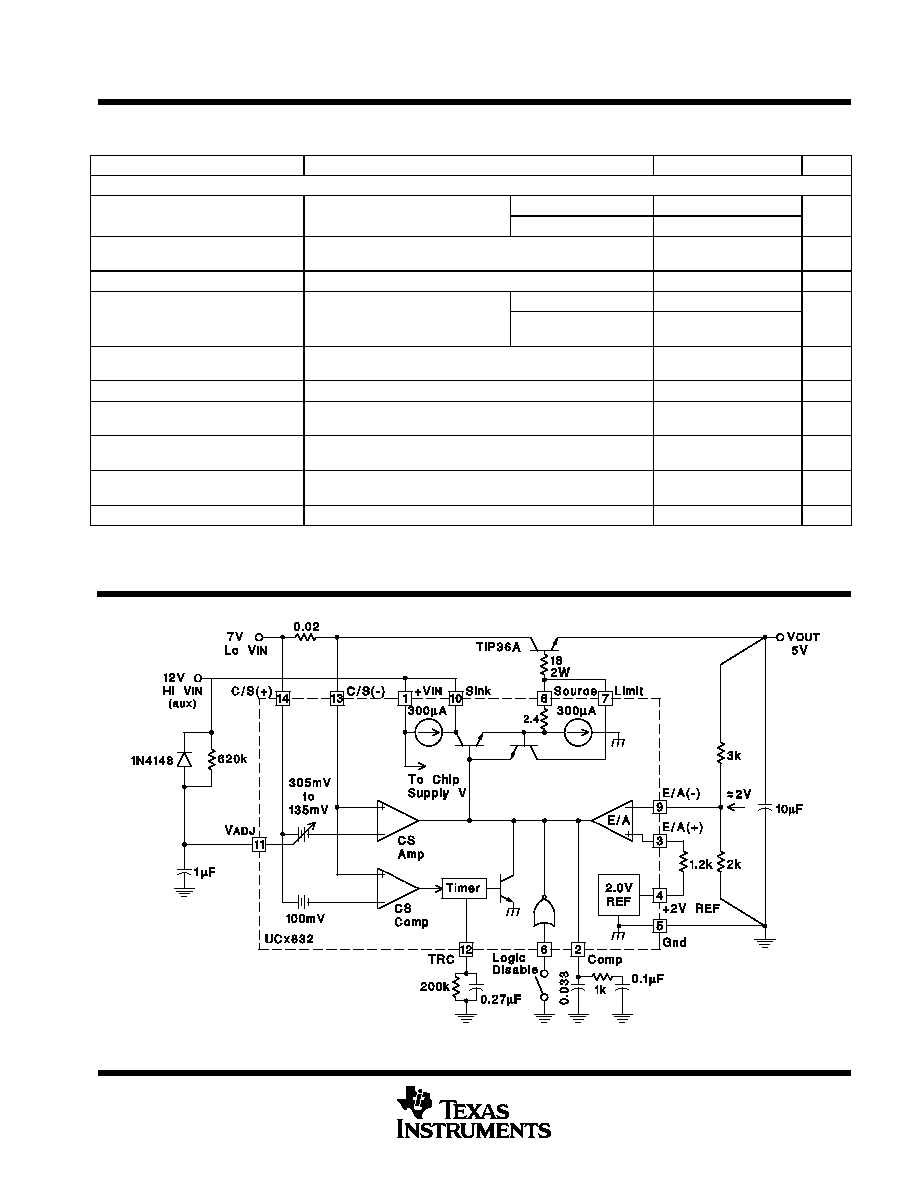
APPLICATION AND OPERATION INFORMATION
Figure 1. NPN Pass (Medium Power, Low Drop-Out Regulator)

UC2832-EP
PRECISION LOW DROPOUT LINEAR CONTROLLER
SGLS147A ≠ JANUARY 2003 ≠ REVISED MARCH 2003
6
POST OFFICE BOX 655303
∑
DALLAS, TEXAS 75265
APPLICATION AND OPERATION INFORMATION
Estimating Maximum Load Capacitance
For any power supply, the rate at which the total output capacitance can be charged depends on the maximum
output current available and on the nature of the load. For a constant-current current-limited power supply, the
output will come up if the load asks for less than the maximum available short-circuit limit current.
To ensure recovery of a duty-ratio current-limited power supply from a short-circuited load condition, there is
a maximum total output capacitance which can be charged for a given unit ON time. The design value of ON
time can be adjusted by changing the timing capacitor. Nominally, T
ON
= 0.693 x 10 k
x C
T
.
Typically, the IC regulates output current to a maximum of I
MAX
= K x I
TH
, where I
TH
is the timer trip-point current,
and
K
+
Current Sense Amplifier Offset Voltage
100 mA
and is variable from 1.35 to 3.05 with V
ADJ
.
For a worst-case constant-current load of value just less than I
TH
, C
MAX
can be estimated from:
C
MAX
+
K
*
1
TH
T
ON
V
OUT
where V
OUT
is the nominal regulator output voltage.
For a resistive load of value R
L
, the value of C
MAX
can be estimated from:
C
MAX
+
T
ON
R
L
1
In
1
*
V
OUT
K
I
TH
R
L
≠1
320
280
260
240
220
200
180
160
300
140
120
Offset V
oltage
≠
mV
0
0.25
0.5
0.75
1
1.25
1.5
1.75
2
2.5
2.25
VADJ (Pin 11) ≠ V
Figure 2. Current Sense Amplifier Offset Voltage vs V
ADJ
UC2832-EP
PRECISION LOW DROPOUT LINEAR CONTROLLER
SGLS147A ≠ JANUARY 2003 ≠ REVISED MARCH 2003
7
POST OFFICE BOX 655303
∑
DALLAS, TEXAS 75265
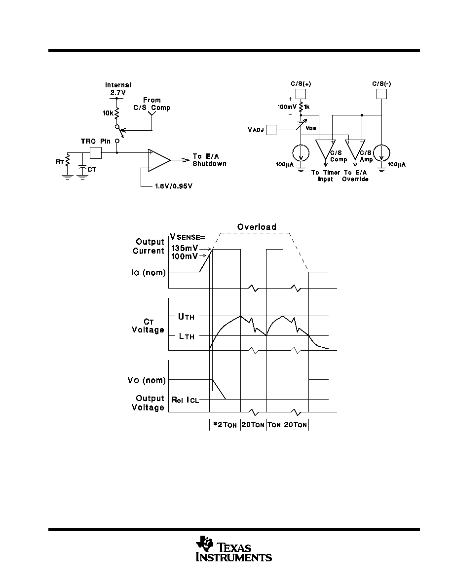
APPLICATION AND OPERATION INFORMATION
Figure 3. Timer Function
Figure 4. Current Sense Input Configuration
NOTE A: VOS = 205 mV to 35 mV
Figure 5. Load Current, Timing Capacitor Voltage, and Output Voltage of the Regulator
Under Fault Conditions

UC2832-EP
PRECISION LOW DROPOUT LINEAR CONTROLLER
SGLS147A ≠ JANUARY 2003 ≠ REVISED MARCH 2003
8
POST OFFICE BOX 655303
∑
DALLAS, TEXAS 75265
APPLICATION AND OPERATION INFORMATION
Figure 6. UCx832 Error Amplifier
Figure 7. UCx832 Current Sense Amplifier
Figure 8. UCx832 Error Amplifier
Figure 9. UCx832 Current Sense Amplifier
UC2832-EP
PRECISION LOW DROPOUT LINEAR CONTROLLER
SGLS147A ≠ JANUARY 2003 ≠ REVISED MARCH 2003
9
POST OFFICE BOX 655303
∑
DALLAS, TEXAS 75265
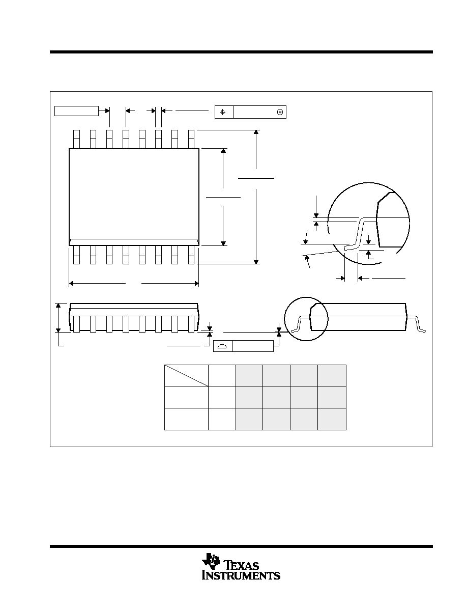
MECHANICAL DATA
DW (R-PDSO-G**)
PLASTIC SMALL-OUTLINE PACKAGE
16 PINS SHOWN
0.419 (10,65)
0.400 (10,15)
0.291 (7,39)
0.299 (7,59)
16
0.400
(10,16)
A MIN
A MAX
(10,41)
0.410
0.462
(11,73)
(11,51)
0.453
18
0.610
(15,49)
(15,24)
0.600
24
DIM
PINS **
4040000/E 08/01
0.104 (2,65) MAX
0.004 (0,10)
0.012 (0,30)
Seating Plane
0
∞
≠ 8
∞
0.016 (0,40)
0.050 (1,27)
16
0.050 (1,27)
1
A
8
9
0.014 (0,35)
0.020 (0,51)
0.010 (0,25) NOM
Gage Plane
0.010 (0,25)
28
0.710
(18,03)
0.700
(17,78)
(12,70)
(12,95)
0.500
20
0.510
0.010 (0,25)
0.004 (0,10)
NOTES: B. All linear dimensions are in inches (millimeters).
C. This drawing is subject to change without notice.
D. Body dimensions do not include mold flash or protrusion not to exceed 0.006 (0,15).
E. Falls within JEDEC MS-013

MECHANICAL DATA
MSOI003E ≠ JANUARY 1995 ≠ REVISED SEPTEMBER 2001
1
POST OFFICE BOX 655303
∑
DALLAS, TEXAS 75265
DW (R-PDSO-G**)
PLASTIC SMALL-OUTLINE PACKAGE
16 PINS SHOWN
0.419 (10,65)
0.400 (10,15)
0.291 (7,39)
0.299 (7,59)
16
0.400
(10,16)
A MIN
A MAX
(10,41)
0.410
0.462
(11,73)
(11,51)
0.453
18
0.610
(15,49)
(15,24)
0.600
24
DIM
PINS **
4040000/E 08/01
0.104 (2,65) MAX
0.004 (0,10)
0.012 (0,30)
Seating Plane
0
∞
≠ 8
∞
0.016 (0,40)
0.050 (1,27)
16
0.050 (1,27)
1
A
8
9
0.014 (0,35)
0.020 (0,51)
0.010 (0,25) NOM
Gage Plane
0.010 (0,25)
28
0.710
(18,03)
0.700
(17,78)
(12,70)
(12,95)
0.500
20
0.510
0.010 (0,25)
0.004 (0,10)
NOTES: A. All linear dimensions are in inches (millimeters).
B. This drawing is subject to change without notice.
C. Body dimensions do not include mold flash or protrusion not to exceed 0.006 (0,15).
D. Falls within JEDEC MS-013

IMPORTANT NOTICE
Texas Instruments Incorporated and its subsidiaries (TI) reserve the right to make corrections, modifications,
enhancements, improvements, and other changes to its products and services at any time and to discontinue
any product or service without notice. Customers should obtain the latest relevant information before placing
orders and should verify that such information is current and complete. All products are sold subject to TI's terms
and conditions of sale supplied at the time of order acknowledgment.
TI warrants performance of its hardware products to the specifications applicable at the time of sale in
accordance with TI's standard warranty. Testing and other quality control techniques are used to the extent TI
deems necessary to support this warranty. Except where mandated by government requirements, testing of all
parameters of each product is not necessarily performed.
TI assumes no liability for applications assistance or customer product design. Customers are responsible for
their products and applications using TI components. To minimize the risks associated with customer products
and applications, customers should provide adequate design and operating safeguards.
TI does not warrant or represent that any license, either express or implied, is granted under any TI patent right,
copyright, mask work right, or other TI intellectual property right relating to any combination, machine, or process
in which TI products or services are used. Information published by TI regarding third≠party products or services
does not constitute a license from TI to use such products or services or a warranty or endorsement thereof.
Use of such information may require a license from a third party under the patents or other intellectual property
of the third party, or a license from TI under the patents or other intellectual property of TI.
Reproduction of information in TI data books or data sheets is permissible only if reproduction is without
alteration and is accompanied by all associated warranties, conditions, limitations, and notices. Reproduction
of this information with alteration is an unfair and deceptive business practice. TI is not responsible or liable for
such altered documentation.
Resale of TI products or services with statements different from or beyond the parameters stated by TI for that
product or service voids all express and any implied warranties for the associated TI product or service and
is an unfair and deceptive business practice. TI is not responsible or liable for any such statements.
Mailing Address:
Texas Instruments
Post Office Box 655303
Dallas, Texas 75265
Copyright
2003, Texas Instruments Incorporated