UC2842AQ, UC2843AQ, UC2844AQ, UC2845AQ
CURRENT-MODE PWM CONTROLLER
SGLS164 ≠ APRIL 2003
1
POST OFFICE BOX 655303
∑
DALLAS, TEXAS 75265
D
Extended Temperature Performance of
≠40
∞
C to 125
∞
C
D
Optimized for Off-line and DC to DC
Converters
D
Low Start Up Current (<0.5 mA)
D
Trimmed Oscillator Discharge Current
D
Automatic Feed Forward Compensation
D
Pulse-by-Pulse Current Limiting
D
Enhanced Load Response Characteristics
D
Under-Voltage Lockout With Hysteresis
D
Double Pulse Suppression
D
High Current Totem Pole Output
D
Internally Trimmed Bandgap Reference
D
500 kHz Operation
D
Low R
O
Error Amp
description
The UC2842A/3A/4A/5A family of control ICs is a pin for pin compatible improved version of the UC2842/3/4/5
family. Providing the necessary features to control current mode switched mode power supplies, this family has the
following improved features. Start up current is guaranteed to be less than 0.5 mA. Oscillator discharge is trimmed
to 8.3 mA. During under voltage lockout, the output stage can sink at least 10 mA at less than 1.2 V for V
CC
over
5 V.
The difference between members of this family are shown in the table below.
PART NUMBER
UVLO ON
UVLO OFF
MAXIMUM DUTY CYCLE
UC2842A
16 V
10 V
<100%
UC2843A
8.5 V
7.9 V
<100%
UC2844A
16 V
10 V
<50%
UC2845A
8.5 V
7.9 V
<50%
Copyright
2003, Texas Instruments Incorporated
PRODUCTION DATA information is current as of publication date.
Products conform to specifications per the terms of Texas Instruments
standard warranty. Production processing does not necessarily include
testing of all parameters.
Please be aware that an important notice concerning availability, standard warranty, and use in critical applications of
Texas Instruments semiconductor products and disclaimers thereto appears at the end of this data sheet.
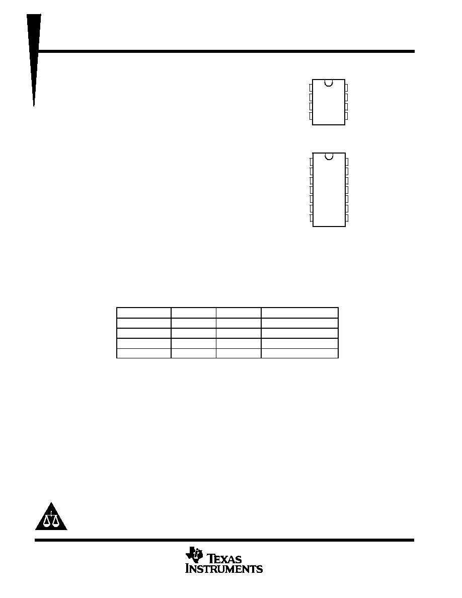
D 8-PIN PACKAGE
(TOP VIEW)
1
2
3
4
8
7
6
5
COMP
V
FB
I
SENSE
R
T
/C
T
V
REF
V
CC
OUTPUT
GND
D 14-PIN PACKAGE
(TOP VIEW)
1
2
3
4
5
6
7
14
13
12
11
10
9
8
COMP
NC
V
FB
NC
I
SENSE
NC
R
T
/C
T
V
REF
NC
V
CC
V
C
OUTPUT
GND
PWR GND
UC2842AQ, UC2843AQ, UC2844AQ, UC2845AQ
CURRENT-MODE PWM CONTROLLER
SGLS164 ≠ APRIL 2003
2
POST OFFICE BOX 655303
∑
DALLAS, TEXAS 75265
ORDERING INFORMATION
TA
PACKAGE
ORDERABLE
PART NUMBER
TOP-SIDE
MARKING
SOIC-8 ≠ D8
Tape and reel
UC2842AQD8R
2842AQ
SOIC-8 ≠ D8
Tube
UC2842AQD8
2842AQ
SOIC-14 ≠ D
Tape and reel
UC2842AQDR
2842AQ
SOIC-14 ≠ D
Tube
UC2842AQD
2842AQ
SOIC-8 ≠ D8
Tape and reel
UC2843AQD8R
2843AQ
SOIC-8 ≠ D8
Tube
UC2843AQD8
2843AQ
SOIC-14 ≠ D
Tape and reel
UC2843AQDR
2843AQ
40
∞
C to 125
∞
C
SOIC-14 ≠ D
Tube
UC2843AQD
2843AQ
≠40
∞
C to 125
∞
C
SOIC-8 ≠ D8
Tape and reel
UC2844AQD8R
2844AQ
SOIC-8 ≠ D8
Tube
UC2844AQD8
2844AQ
SOIC-14 ≠ D
Tape and reel
UC2844AQDR
2844AQ
SOIC-14 ≠ D
Tube
UC2844AQD
2844AQ
SOIC-8 ≠ D8
Tape and reel
UC2845AQD8R
2845AQ
SOIC-8 ≠ D8
Tube
UC2845AQD8
2845AQ
SOIC-14 ≠ D
Tape and reel
UC2845AQDR
2845AQ
SOIC-14 ≠ D
Tube
UC2845AQD
2845AQ
Package drawings, standard packing quantities, thermal data, symbolization, and PCB design guidelines
are available at www.ti.com/sc/package.
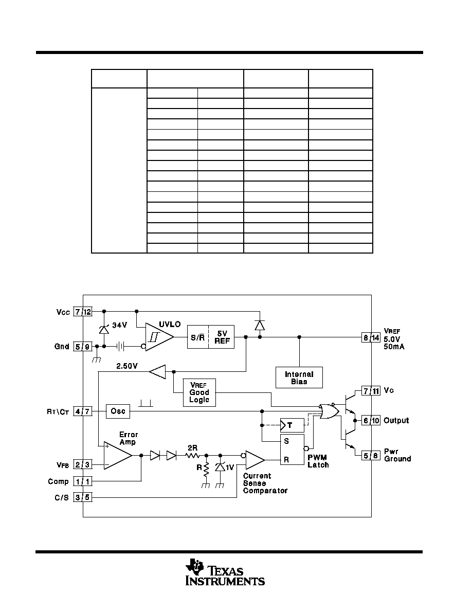
block diagram
NOTES:
1. A = DIL-8 Pin Number. B = SO-14 Pin Number.
2. Toggle flip flop used only in 2844A and 2845A.
UC2842AQ, UC2843AQ, UC2844AQ, UC2845AQ
CURRENT-MODE PWM CONTROLLER
SGLS164 ≠ APRIL 2003
3
POST OFFICE BOX 655303
∑
DALLAS, TEXAS 75265
Ordering Information
UC
4
Q
PACKAGE
D = Plastic SOIC, 14 pin
D8 = Plastic SOIC, 8 pin
PRODUCT OPTION
2 through 5
AUTOMOTIVE TEMPERATURE RANGE INDICATOR
D
TAPE and REEL INDICATOR
R
284
A
IMPROVED PERFORMANCE INDICATOR
UC2842AQ, UC2843AQ, UC2844AQ, UC2845AQ
CURRENT-MODE PWM CONTROLLER
SGLS164 ≠ APRIL 2003
4
POST OFFICE BOX 655303
∑
DALLAS, TEXAS 75265
absolute maximum ratings over operating free-air temperature range (unless otherwise noted)
V
CC
voltage (low impedance source)
30 V
. . . . . . . . . . . . . . . . . . . . . . . . . . . . . . . . . . . . . . . . . . . . . . . . . . . . . . . . .
V
CC
voltage (I
CC
mA)
self limiting
. . . . . . . . . . . . . . . . . . . . . . . . . . . . . . . . . . . . . . . . . . . . . . . . . . . . . . . . . . . . . . . .
Output current, I
O
±
1 A
. . . . . . . . . . . . . . . . . . . . . . . . . . . . . . . . . . . . . . . . . . . . . . . . . . . . . . . . . . . . . . . . . . . . . . . . .
Output energy (capacitive load)
5
µ
J
. . . . . . . . . . . . . . . . . . . . . . . . . . . . . . . . . . . . . . . . . . . . . . . . . . . . . . . . . . . . . .
Analog Inputs (pins 3, 5)
≠0.3 V to 6.3 V
. . . . . . . . . . . . . . . . . . . . . . . . . . . . . . . . . . . . . . . . . . . . . . . . . . . . . . . . . . .
Error Amp Output Sink current
10 mA
. . . . . . . . . . . . . . . . . . . . . . . . . . . . . . . . . . . . . . . . . . . . . . . . . . . . . . . . . . . . .
Power Dissipation at T
A
< +25
_
C (D package)
1 W
. . . . . . . . . . . . . . . . . . . . . . . . . . . . . . . . . . . . . . . . . . . . . . . . . .
Package thermal impedance,
JA
(see Note 1): D (8-pin) package
97
∞
C/W
. . . . . . . . . . . . . . . . . . . . . . . . . . . .
Storage temperature range, T
stg
≠65
_
C to 150
_
C
. . . . . . . . . . . . . . . . . . . . . . . . . . . . . . . . . . . . . . . . . . . . . . . . . . . .
Lead temperature soldering 1,6 mm (1/16 inch) from case for 10 seconds
260
_
C
. . . . . . . . . . . . . . . . . . . . . . .
Stresses beyond those listed under "absolute maximum ratings" may cause permanent damage to the device. These are stress ratings only, and
functional operation of the device at these or any other conditions beyond those indicated under "recommended operating conditions" is not implied.
Exposure to absolute-maximum-rated conditions for extended periods may affect device reliability.
Unless otherwise indicated, voltages are reference to ground and currents are positive into and negative out of the specified terminals.
NOTE 1: Long term high≠temperature storage and/or extended use at maximum recommended operating conditions may result in a reduction of
overall device life. See http://www.ti.com/ep_quality for additional information on enhanced plastic packaging.
electrical characteristics, T
A
= ≠40
_
C to 125
_
C, V
CC
= 15 V (see Note 1), R
T
= 10 k
, C
T
= 3.3 nF, and
T
A
= T
J
(unless otherwise stated)
PARAMETER
TEST CONDITIONS
MIN
TYP
MAX
UNITS
Reference Section
Output voltage
TJ = 25
_
C,
IO = 1 mA
4.95
5.0
5.05
V
Line regulation voltage
VIN = 12 V to 25 V
6
20
mV
Load regulation voltage
IO = 1 mA to 20 mA
6
25
mV
Temperature stability
See Notes 2 and 3
0.2
0.4
mV/
_
C
Total output variation voltage
Line, Load, Temp.
4.9
5.1
V
Output noise voltage
f = 10 Hz to 10 kHz,
See Note 2
TJ = 25
_
C
50
µ
V
Long term stability
1000 hours,
See Note 2
TA = 125
_
C
5
25
mV
Output short-circuit current
≠30
≠100
≠180
mA
Oscillator Section
Initial accuracy
See Note 4
TJ = 25
_
C
47
52
57
kHz
Voltage stability
VCC = 12 V to 25 V
0.2
1
%
Temperature stability
TA = MIN to MAX, See Note 2
5
%
Amplitude peak-to-peak
V pin 7,
See Note 2
1.7
V
Discharge current
V pin 7
2 V
See Note 5
TJ = 25
_
C
7.8
8.3
8.8
mA
Discharge current
V pin 7 = 2 V,
See Note 5
TJ = Full range
7.5
8.8
mA
UC2842AQ, UC2843AQ, UC2844AQ, UC2845AQ
CURRENT-MODE PWM CONTROLLER
SGLS164 ≠ APRIL 2003
5
POST OFFICE BOX 655303
∑
DALLAS, TEXAS 75265
electrical characteristics, T
A
= ≠40
_
C to 125
_
C, V
CC
= 15 V (see Note 1), R
T
= 10 k
, C
T
= 3.3 nF, and
T
A
= T
J
(unless otherwise stated)
PARAMETER
TEST CONDITIONS
MIN
TYP
MAX
UNITS
Error Amplifier Section
Input voltage
COMP = 2.5 V
2.45
2.5
2.55
V
Input bias current
≠0.3
≠1
µ
A
Open loop voltage gain (AVOL)
VO = 2 V to 4 V
65
90
dB
Unity gain bandwidth
See Note 2
TJ = 25
_
C
0.7
1
MHz
PSRR
VCC = 12 V to 25 V
60
70
dB
Output sink current
FB = 2.7 V,
COMP = 1.1 V
2
6
mA
Output source current
FB = 2.3 V,
COMP = 5 V
≠0.5
≠0.8
mA
VOUT high
FB = 2.3 V,
RL = 15 k
to GND
5
6
V
VOUT low
FB = 2.7 V,
RL = 15 k
to VREF
0.7
1.1
V
Current Sense Section
Gain
See Notes 6 and 7
2.85
3
3.15
V/V
Maximum input signal
COMP = 5 V,
See Note 6
0.9
1
1.1
V
PSRR
VCC = 12 V to 25 V,See Note 6
70
dB
Input bias current
≠2
≠10
µ
A
Delay to output
ISENSE = 0 V to 2 V,
See Note 2
150
300
ns
Output Section (OUT)
Low level output voltage
IOUT = 20 mA
0.1
0.4
V
Low-level output voltage
IOUT = 200 mA
15
2.2
V
High level output voltage
IOUT = ≠20 mA
13
13.5
V
High-level output voltage
IOUT = ≠200 mA
12
13.5
V
Rise time
CL = 1 nF,
See Note 2
TJ = 25
_
C
50
150
ns
Fall time
CL = 1 nF,
See Note 2
TJ = 25
_
C
50
150
ns
UVLO saturation
VCC = 5 V,
IOUT = 10 mA
0.7
1.2
V
Undervoltage Lockout Section
Start threshold
UC2842A,
UC2844A
15
16
17
V
Start threshold
UC2843A,
UC2845A
7.8
8.4
9
V
Minimum operation voltage after turn on
UC2842A,
UC2844A
9
10
11
V
Minimum operation voltage after turn on
UC2843A,
UC2845A
7
7.6
8.2
V
UC2842AQ, UC2843AQ, UC2844AQ, UC2845AQ
CURRENT-MODE PWM CONTROLLER
SGLS164 ≠ APRIL 2003
6
POST OFFICE BOX 655303
∑
DALLAS, TEXAS 75265
electrical characteristics, T
A
= ≠40
_
C to 125
_
C, V
CC
= 15 V (see Note 1), R
T
= 10 k
, C
T
= 3.3 nF, and
T
A
= T
J
(unless otherwise stated)
PARAMETER
TEST CONDITIONS
MIN
TYP
MAX
UNITS
PWM Section
Maximum duty cycle
UC2842A, UC2843A
94
96
100
%
Maximum duty cycle
UC2844A, UC2845A
47
48
50
%
Minimum duty cycle
0
%
Total Standby Current
Start-up current
0.3
0.5
mA
Operating supply current
FB = 0 V,
SENSE = 0 V
11
17
mA
VCC internal zener voltage
ICC = 25 mA
30
34
V
NOTES:
1. Adjust VCC above the start threshold before setting at 15 V.
2. Not production tested.
3. Temperature stability, sometimes referred to as average temperature coefficient, is described by the equation:
Temp Stability =
VREF (max) ≠ VREF (min)
TJ (max) ≠ TJ (min)
. VREF (max) and VREF (min) are the maximum and minimum reference voltage measured
over the appropriate temperature range. Note that the extremes in voltage do not necessarily occur at the extremes in temperature.
4. Output frequency equals oscillator frequency for the UC2842A and UC2843A. Output frequency is one half oscillator frequency for the
UC2844A and UC2845A.
5. This parameter is measured with RT = 10 k
to VREF. This contributes approximately 300
µ
A of current to the measurement. The total
current flowing into the RT/C pin will be approximately 300
µ
A higher than the measured value.
6. Parameter measured at trip point of latch with VFB at 0 V.
7. Gain is defined by:
A =
D
VCOMP
D
VSENSE
; 0
v
VSENSE
v
0.8 V.
PA
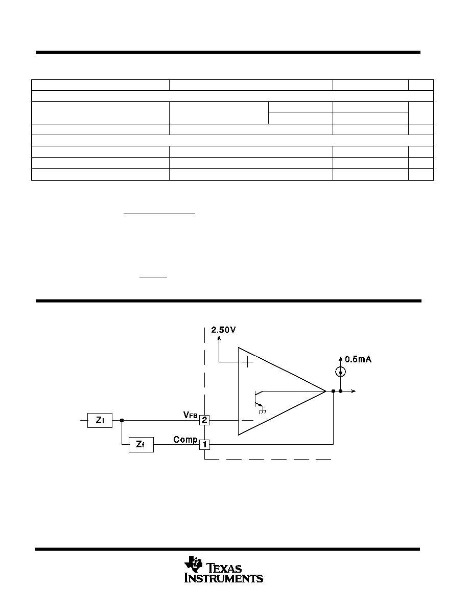
RAMETER MEASUREMENT INFORMATION
Error Amp can source and sink up to 0.5 mA, and sink up to 2 mA.
Figure 1. Error Amp Configuration

UC2842AQ, UC2843AQ, UC2844AQ, UC2845AQ
CURRENT-MODE PWM CONTROLLER
SGLS164 ≠ APRIL 2003
7
POST OFFICE BOX 655303
∑
DALLAS, TEXAS 75265
PARAMETER MEASUREMENT INFORMATION
During UVLO, the Output is low.
Figure 2. Under Voltage Lockout
Peak Current (Is) is Determined By The Formula:
Ismax
1.0V
RS
A small RC filter may be required to supress switch transients.
Figure 3. Current Sense Circuit
UC2842AQ, UC2843AQ, UC2844AQ, UC2845AQ
CURRENT-MODE PWM CONTROLLER
SGLS164 ≠ APRIL 2003
8
POST OFFICE BOX 655303
∑
DALLAS, TEXAS 75265
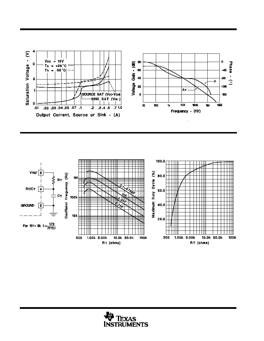
PARAMETER MEASUREMENT INFORMATION
Figure 4
Output Saturation Characteristics
Figure 5
Error Amplifier Open-Loop Frequency Response
AP
PLICATION INFORMATION
Oscillator Frequency vs Timing Resistance
Maximum Duty Cycle vs Timing Resistor
Figure 6. Oscillator
UC2842AQ, UC2843AQ, UC2844AQ, UC2845AQ
CURRENT-MODE PWM CONTROLLER
SGLS164 ≠ APRIL 2003
9
POST OFFICE BOX 655303
∑
DALLAS, TEXAS 75265
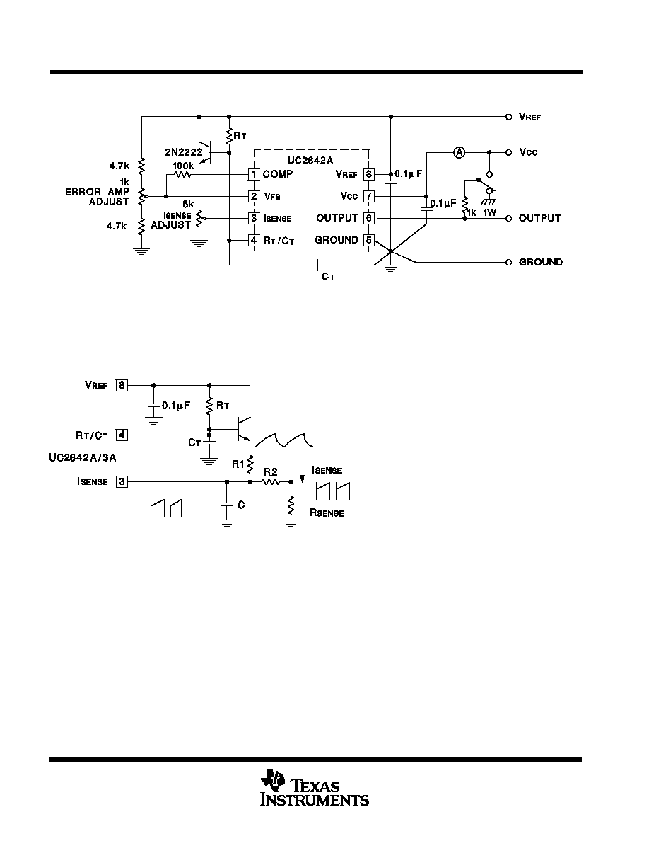
APPLICATION INFORMATION
High peak currents associated with capacitive loads necessitate careful grounding techniques. Timing and bypass capacitors should be
connected close to pin 5 in a single point ground. The transistor and 5k potentiometer are used to sample the oscillator waveform and apply an
adjustable ramp to pin 3.
Figure 7. Open-Loop Laboratory Text Fixture
A fraction of the oscillator ramp can be resistively summed
with the current sense signal to provide slope compensation
for converters requiring duty cycles over 50%.
Note that capacitor, C, forms a filter with R2 to suppress the
leading edge switch spikes.
Figure 8. Slope Complression
UC2842AQ, UC2843AQ, UC2844AQ, UC2845AQ
CURRENT-MODE PWM CONTROLLER
SGLS164 ≠ APRIL 2003
10
POST OFFICE BOX 655303
∑
DALLAS, TEXAS 75265
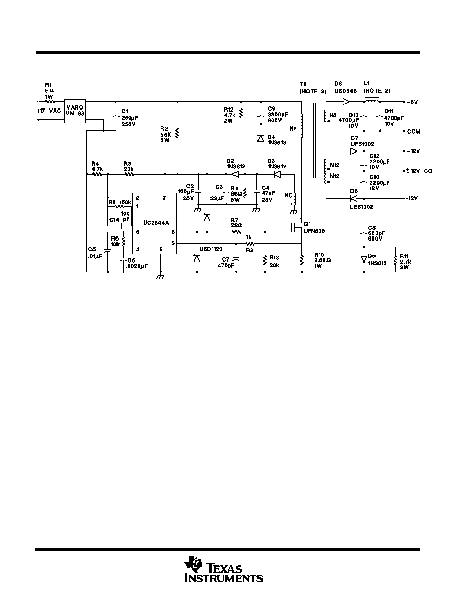
APPLICATION INFORMATION
Power Supply Specifications
1. Input Voltage
95VAC to 130VAC (50Hz/60Hz)
2. Line Isolation
3750V
3. Switching Frequency
40 kHz
4. Efficiency, Full Load
70%
5. Output Voltage:
A. +5V,
±
5%; 1A to 4A Load
B. +12V,
±
3%; 0.1A to 0.3A Load Ripple voltage: 100 mV P-P Max
C. ≠12V,
±
3%; 0.1A to 0.3A Load Ripple voltage: 100 mV P-P Max
Figure 9. Off-Line Flyback Regulator


IMPORTANT NOTICE
Texas Instruments Incorporated and its subsidiaries (TI) reserve the right to make corrections, modifications,
enhancements, improvements, and other changes to its products and services at any time and to discontinue
any product or service without notice. Customers should obtain the latest relevant information before placing
orders and should verify that such information is current and complete. All products are sold subject to TI's terms
and conditions of sale supplied at the time of order acknowledgment.
TI warrants performance of its hardware products to the specifications applicable at the time of sale in
accordance with TI's standard warranty. Testing and other quality control techniques are used to the extent TI
deems necessary to support this warranty. Except where mandated by government requirements, testing of all
parameters of each product is not necessarily performed.
TI assumes no liability for applications assistance or customer product design. Customers are responsible for
their products and applications using TI components. To minimize the risks associated with customer products
and applications, customers should provide adequate design and operating safeguards.
TI does not warrant or represent that any license, either express or implied, is granted under any TI patent right,
copyright, mask work right, or other TI intellectual property right relating to any combination, machine, or process
in which TI products or services are used. Information published by TI regarding third-party products or services
does not constitute a license from TI to use such products or services or a warranty or endorsement thereof.
Use of such information may require a license from a third party under the patents or other intellectual property
of the third party, or a license from TI under the patents or other intellectual property of TI.
Reproduction of information in TI data books or data sheets is permissible only if reproduction is without
alteration and is accompanied by all associated warranties, conditions, limitations, and notices. Reproduction
of this information with alteration is an unfair and deceptive business practice. TI is not responsible or liable for
such altered documentation.
Resale of TI products or services with statements different from or beyond the parameters stated by TI for that
product or service voids all express and any implied warranties for the associated TI product or service and
is an unfair and deceptive business practice. TI is not responsible or liable for any such statements.
Following are URLs where you can obtain information on other Texas Instruments products and application
solutions:
Products
Applications
Amplifiers
amplifier.ti.com
Audio
www.ti.com/audio
Data Converters
dataconverter.ti.com
Automotive
www.ti.com/automotive
DSP
dsp.ti.com
Broadband
www.ti.com/broadband
Interface
interface.ti.com
Digital Control
www.ti.com/digitalcontrol
Logic
logic.ti.com
Military
www.ti.com/military
Power Mgmt
power.ti.com
Optical Networking
www.ti.com/opticalnetwork
Microcontrollers
microcontroller.ti.com
Security
www.ti.com/security
Telephony
www.ti.com/telephony
Video & Imaging
www.ti.com/video
Wireless
www.ti.com/wireless
Mailing Address:
Texas Instruments
Post Office Box 655303 Dallas, Texas 75265
Copyright
2004, Texas Instruments Incorporated