UC1854B
UC2854A, UC2854B
UC3854A, UC3854B
SLUS329A - JUNE 1998 - REVISED AUGUST 2003
ADVANCED HIGH POWER FACTOR
PREREGULATOR
1
www.ti.com
FEATURES
D
Controls Boost PWM to Near-Unity Power
Factor
D
Limits Line Current Distortion To < 3%
D
World-Wide Operation Without Switches
D
Accurate Power Limiting
D
Fixed-Frequency Average Current-Mode
Control
D
High Bandwidth (5 MHz), Low-Offset Current
Amplifier
D
Integrated Current- and Voltage Amplifier
Output Clamps
D
Multiplier Improvements: Linearity, 500 mV
V
AC
Offset (Eliminates External Resistor), 0 V
to 5 V Multout Common-Mode Range
D
V
REF
GOOD Comparator
D
Faster and Improved Accuracy ENABLE
Comparator
D
UVLO Options (16 V/10 V or 10.5 V/10 V)
D
300-
�
A Start-Up Supply Current
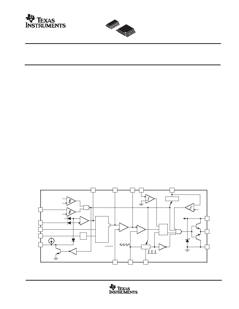
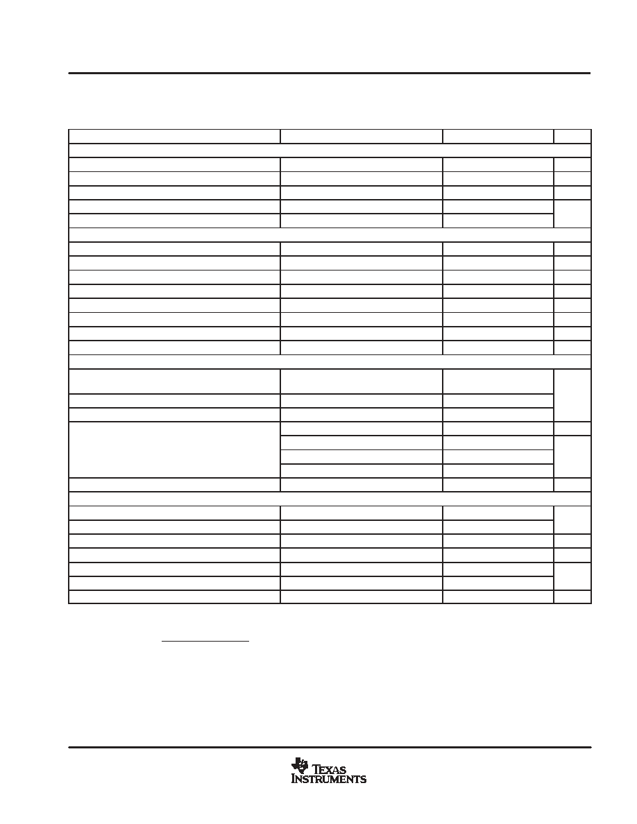
BLOCK DIAGRAM
DESCRIPTION
The UC3854A/B products are pin compatible
enhanced versions of the UC3854. Like the
UC3854, these products provide all of the
functions necessary for active power factor
corrected preregulators. The controller achieves
near unity power factor by shaping the AC input
line current waveform to correspond to the AC
input line voltage. To do this the UC3854A/B uses
average current mode control. Average current
mode control maintains stable, low distortion
sinusoidal line current without the need for slope
compensation, unlike peak current mode control.
A 1% 7.5 V reference, fixed frequency oscillator,
PWM, voltage amplifier with soft-start, line voltage
feedforward (V
RMS
squarer), input supply voltage
clamp, and over current comparator round out the
list of features.
Available in the 16-pin N (PDIP), DW (SOIC-
Wide), and J (CDIP) and 20-pin Q (PLCC)
package. See ordering information on page 3 for
availability by temperature range.
UDG-03110
10
11
6
8
15
1
16
ENA
VSENSE
IAC
VRMS
VCC
GND
GTDRV
2.65 V / 2.15 V
3 V
7
VAO
13
VRMS
X2
A
B
C
(A) 16 V / 10 V
(B) 10.5 V / 10 V
5
MOUT
4
ISENSE
3
CAO
14
CT
OSC
12
RSET
S
Q
R
R
2
PKLMT
20 V
IC
POWER
7.5 V REF
9
REF
RUN
7.1 V
RUN
VCC
14
�
A
I
MOUT
+
A
B
C
PRODUCTION DATA information is current as of publication date.
Products conform to specifications per the terms of Texas Instruments
standard warranty. Production processing does not necessarily include
testing of all parameters.
Copyright
2003, Texas Instruments Incorporated
UC1854B
UC2854A, UC2854B
UC3854A, UC3854B
SLUS329A - JUNE 1998 - REVISED AUGUST 2003
2
www.ti.com
DESCRIPTION (continued)
The UC3854A/B products improve upon the UC3854 by offering a wide bandwidth, low offset current amplifier,
a faster responding and improved accuracy enable comparator, a VREF GOOD comparator, UVLO threshold
options (16 V/10 V for offline, 10.5 V/10 V for startup from an auxiliary 12 V regulator), lower startup supply
current, and an enhanced multiply/divide circuit. New features like the amplifier output clamps, improved
amplifier current sinking capability, and low offset VAC pin reduce the external component count while improving
performance. Improved common mode input range of the multiplier output/current amplifier input allow the
designer greater flexibility in choosing a method for current sensing. Unlike its predecessor, R
SET
controls only
oscillator charging current and has no effect on clamping the maximum multiplier output current. This current
is now clamped to a maximum of 2
�
I
AC
at all times which simplifies the design process and provides foldback
power limiting during brownout and extreme low line conditions.
These devices have limited built-in ESD protection. The leads should be shorted together or the device placed in conductive foam
during storage or handling to prevent electrostatic damage to the MOS gates.
ABSOLUTE MAXIMUM RATINGS
over operating free-air temperature range unless otherwise noted(1)
UCX854A, UCX854B
UNIT
Supply voltage, VCC
22
V
GTDRV current, IGTDRV
Continuous
0.5
A
GTDRV Current, IGTDRV
50% duty cycle
1.5
A
Input voltage
VSENSE, VRMS, ISENSE MOUT
11
V
Input voltage
PKLMT
5
V
Input current
RSET, IAC, PKLMT, ENA
10
mA
Power dissipation
1
W
Junction temperature, TJ
-55 to 150
Storage temperature, Tstg
-65 to 150
�
C
Lead temperature, Tsol, 1,6 mm (1/16 inch) from case for 10 seconds
300
C
(1) Stresses beyond those listed under "absolute maximum ratings" may cause permanent damage to the device. These are stress ratings only,
and functional operation of the device at these or any other conditions beyond those indicated under "recommended operating conditions" is
not implied. Exposure to absolute-maximum-rated conditions for extended periods may affect device reliability. All voltages are with respect to
GND. Currents are positive into and negative out of, the specified terminal. ENA input is internally clamped to approximately 10 V.
RECOMMENDED OPERATING CONDITIONS
MIN
MAX
UNIT
Supply voltage, VCC
10
20
V
UC1854X
-55
125
Operating junction temperature, TJ
UC2854X
-40
85
�
C
Operating junction temperature, TJ
UC3854X
0
70
C
UC1854B
UC2854A, UC2854B
UC3854A, UC3854B
SLUS329A - JUNE 1998 - REVISED AUGUST 2003
3
www.ti.com
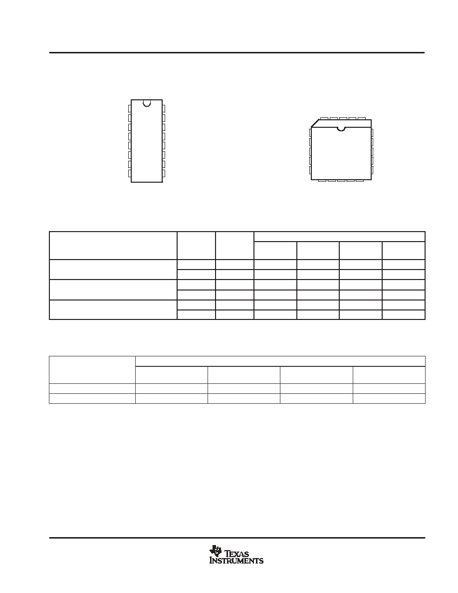
PACKAGE DESCRIPTION
1
2
3
4
5
6
7
8
16
15
14
13
12
11
10
9
GND
PKLMT
CAO
ISENSE
MOUT
IAC
VAO
VRMS
GTDRV
VCC
CT
SS
RSET
VSENSE
ENA
VREF
J, N and DW PACKAGES
(TOP VIEW)
5
4
6
7
8
18
17
16
15
14
ISENSE
CAOUT
N/C
MOUT
IAC
CT
SS
N/C
RSET
VSENSE
3 2 1 20 19
9 10 11 12 13
PKLMT
GND
N/C
GTDR
V
VCC
VA
O
VRMS
NC
VREF
ENA
Q PACKAGE
(TOP VIEW)
N/C - No connection
ORDERING INFORMATION
UVLO
UVLO
PART NUMBERS
TA
UVLO
TURN-ON
(V)
UVLO
TURN-OFF
(V)
CDIP-16
(J)
PDIP-16
(N)
SOIC-16
(DW)
PLCC-20
(Q)
-55
�
C to 125
�
C
16
10
-
-
-
-
-55
�
C to 125
�
C
10.5
10
UC1854BJ
-
-
-
-40
�
C to 85
�
C
16
10
UC2854AJ
UC2854AN
UC2854ADW
UC2854AQ
-40
�
C to 85
�
C
10.5
10
UC2854BJ
UC2854BN
UC2854BDW
UC2854BQ
0
�
C to 70
�
C
16
10
-
UC3854AN
UC3854ADW
-
0
�
C to 70
�
C
10.5
10
-
UC3854BN
UC3854BDW
-
(1) The DW and Q packages are available taped and reeled. Add TR suffix to device type (e.g. UC2854ADWTR) to order quantities of 2,000
devices per reel for the DW package and 1,000 devices per reel for the Q package.
THERMAL RESISTANCE
PACKAGED DEVICES
RESISTANCES
CDIP-16
(J)
PDIP-16
(N)
SOP-16
(DW)
PLCC-20
(Q)
JC (
�
C/W)
28(2)
45
27
34
JA (
�
C/W)
80-120
90(3)
50-130(3)
43-75(3)
(2)
JC data values stated are derived from MIL-STD-1835B which states "the baseline values shown are worst case (mean +2s) for a 60
�
60
mil microcircuit device silicon die and applicable for devices with die sizes up to 14,400 square mils. For device die sizes greater than
14,400 square mils use the following values, dual-in-line, 11
�
C/W; flat pack and pin grid array, 10
�
C/W.
(3)
JA (junction-to-ambient) applies to devices mounted to five square inch FR4 PC board with one ounce copper where noted. When
resitance range is given, lower values are for five square inch aluminum PC board. Test PWB is 0.062 inches thick and typically uses
0.635 mm trace widths for power packages and 1.3 mm trace widths for non-power packages with a 100
�
100 mil probe land are at the
end of each trace.
UC1854B
UC2854A, UC2854B
UC3854A, UC3854B
SLUS329A - JUNE 1998 - REVISED AUGUST 2003
4
www.ti.com
ELECTRICAL CHARACTERISTICS
VCC = 18 V, RT = 8.2 k
, CT = 1.5 nF, VPKLMT = 1 V, VVRMS = 1.5 V, IIAC = 100
�
A, IISENSE = 0 V, VCAO = 3.5 V, VVAO = 5 V, VVSENSE = 3 V,
-40
�
C < TA < 85
�
C for the UC2854A and UC2854B, and 0
�
C < TA <70
�
C for the UC3854A and UC3854B, and TA = TJ (unless otherwise
noted)
PARAMETER
TEST CONDITIONS
MIN
TYP
MAX
UNIT
OVERALL
Supply current, off
CAO = 0 V,
VAO = 0 V,
VCC = VUVLO-0.3 V
250
400
�
A
Supply current, on
12
18
mA
VCC turn-on threshold voltage
UCx854A
15.0
16.0
17.5
VCC turn-on threshold voltage
UCx854B
8.0
10.5
11.2
V
VCC turn-off threshold voltage
9
10
12
V
VCC clamp
IVCC = IVCC(on) + 5 mA
18
20
22
VOLTAGE AMPLIFIER
Input voltage
2.9
3.0
3.1
V
VSENSE bias current
-500
-25
500
nA
Open loop gain
2 V
VOUT
5 V
70
100
dB
VOH
High-level output voltage
ILOAD = -500
�
A
6
V
VOL
Low-level output voltage
ILOAD = 500
�
A
0.3
0.5
V
ISC
Output short-circuit current
VOUT = 0 V
1.5
4.5
mA
Gain bandwidth product(1)
fIN = 100 kHz,
10 mVP-P
1
MHz
CURRENT AMPLIFIER
Input offset voltage
VCM = 0 V,
TA = 25
�
C
-4
0
mV
Input offset voltage
VCM = 0 V,
overtemperature
-5.5
0
mV
Input bias current, ISENSE
VCM = 0 V
-500
500
nA
Open loop gain
2 V
VOUT
6 V
80
110
dB
VOH
High-level output voltage
ILOAD = -500
�
A
8
V
VOL
Low-level output voltage
ILOAD = 500
�
A
0.3
0.5
V
ISC
Output short-circuit current
VOUT = 0 V
1.5
4.5
mA
CMRR
Common mode rejection range
-0.3
5.0
V
Gain bandwidth product(1)
fIN = 100 kHz,
10 mVP-P
3
5
MHz
REFERENCE
Output voltage
IREF = 0 mA,
TA = 25
�
C
7.4
7.5
7.6
V
Output voltage
IREF = 0 mA
7.35
7.50
7.65
V
Load regulation
1 mA
IREF
10 mA
0
8
20
mV
Line regulation
12 V
VCC
18 V
0
14
25
mV
ISC
Short circuit current
VREF = 0 V
25
35
60
mA
(1) Ensured by design. Not production tested.
(2) Gain constant. (K)
+
I
IAC
V
VAO
*
1.5 V
V
VRMS
2
I
MOUT
UC1854B
UC2854A, UC2854B
UC3854A, UC3854B
SLUS329A - JUNE 1998 - REVISED AUGUST 2003
5
www.ti.com
ELECTRICAL CHARACTERISTICS
VCC = 18 V, RT = 8.2 k
, CT = 1.5 nF, VPKLMT = 1 V, VVRMS = 1.5 V, IIAC = 100
�
A, IISENSE = 0 V, VCAO = 3.5 V, VVAO = 5 V, VVSENSE = 3 V,
-40
�
C < TA < 85
�
C for the UC2854A and UC2854B, and 0
�
C < TA <70
�
C for the UC3854A and UC3854B, and TA = TJ (unless otherwise
noted)
PARAMETER
TEST CONDITIONS
MIN
TYP
MAX
UNIT
OSCILLATOR
Initial accuracy
TA = 25
�
C
85
100
115
kHz
Voltage stability
12 V
VCC
18 V
1%
Total variation
Line, temperature
80
120
kHz
Ramp amplitude (peak-to-peak)
4.9
5.9
V
Ramp valley voltage
0.8
1.3
V
ENABLE/SOFT-START/CURRENT LIMIT
Enable threshold voltage
2.35
2.55
2.80
V
Enable hysteresis
VFAULT = 2.5 V
500
600
mV
Enable input bias current
VENA = 0 V
-2
-5
�
A
Propagation delay to disable time(1)
Enable overdrive = 100 mV
300
ns
Soft-start charge current
VSS = 2.5 V
10
14
24
Peak limit offset voltage
-15
15
mV
Peak limit input current
VPKLMT = -0.1 V
-200
-100
�
A
Peak limit propagation delay time(1)
150
ns
MULTIPLIER
Output current, IAC limited
IAC = 100
�
A,
VRMS = 1 V,
RSET = 10 k
-220
-200
-170
A
Output current, zero
IAC = 0
�
A,
RSET = 10 k
-2.0
-0.2
2.0
�
A
Output current, power limited
VRMS = 1.5 V,
Va = 6 V
-230
-200
-170
VRMS = 1.5 V,
Va = 2 V
-22
�
A
Output current
VRMS = 1.5 V,
Va = 5 V
-156
Output current
VRMS = 5 V,
Va = 2 V
-2
�
A
VRMS = 5 V,
Va = 5 V
-14
�
A
Gain constant(2)
VRMS = 1.5 V, Va = 6V, TA = 25
�
C
-1.1
-1.0
-0.9
A/A
GATE DRIVER
VOH
High-level output voltage
IOUT = -200 mA,
VCC = 15 V
12.0
12.8
V
VOL
Low-level output voltage
IOUT = 200 mA
1.0
2.2
V
IOUT = 10 mA
300
500
mV
Low-level UVLO voltage
IOUT = 50 mA,
VCC = 0 V
0.9
1.5
V
Output rise time(1)
CLOAD = 1 nF
35
ns
Output fall time(1)
CLOAD = 1 nF
35
ns
Output peak current(1)
CLOAD = 10 nF
1.0
A
(1) Ensured by design. Not production tested.
(2) Gain constant. (K)
+
I
IAC
V
VAO
*
1.5 V
V
VRMS
2
I
MOUT

UC1854B
UC2854A, UC2854B
UC3854A, UC3854B
SLUS329A - JUNE 1998 - REVISED AUGUST 2003
6
www.ti.com
TERMINAL FUNCTIONS
TERMINAL
NAME
PACKAGES
I/O
DESCRIPTION
NAME
J/N/DW
Q/L
I/O
DESCRIPTION
CAO
3
4
O
Output of the wide bandwidth current amplifier and one of the inputs to the PWM duty-cycle
comparator. The output signal generated by this amplifier commands the PWM to force the correct
input current. The output can swing from 0.1 V to 7.5 V.
CT
14
18
I
Capacitor from CT to GND sets the PWM oscillator frequency
ENA
10
13
I
A nominal voltage above 2.65 V on this pin allows the device to begin operating. Once operating,
the device shuts off if this pin goes below 2.15 V nominal.
GND
1
2
-
All bypass and timing capacitors connected to GND should have leads as short and direct as
possible. All voltages are measured with respect GND.
GTDRV
16
20
O
Output of the PWM is a 1.5-A peak totem-pole MOSFET gate driver on GTDRV. This output is
internally clamped to 15 V so that the device can be operated with VCC as high as 35 V. Use a
series gate resistor of at least 5
to prevent interaction between the gate impedance and the
GTDRV output driver that might cause the GTDRV output to overshoot excessively. Some
overshoot of the GTDRV output is always expected when driving a capacitive load.
IAC
6
8
I
Current input to the multiplier, proportional to the instantaneous line voltage. This input to the
analog multiplier is a current. The multiplier is tailored for very low distortion from this current input
(IAC) to MOUT, so this is the only multiplier input that should be used for sensing instantaneous
line voltage. The nominal voltage on IAC is 6 V, so in addition to a resistor from IAC to rectified
60 Hz, connect a resistor from IAC to VREF. If the resistor to VREF is one-fourth of the value of the
resistor to the rectifier, then the 6-V offset is cancelled, and the line current has minimal cross-over
distortion.
ISENSE
4
5
I
Switch current sensing input. This is the inverting input to the current amplifier. This input and the
non-inverting input MOUT remain functional down to and below GND. Care should be taken to
avoid taking these inputs below -0.5V, because they are protected with diodes to GND.
MOUT
5
7
I/O
Multiplier output and current sense plus. The output of the analog multiplier and the non-inverting
input of the current amplifier are connected together at MOUT. The cautions about taking ISENSE
below -0.5V also apply to MOUT. As the multiplier output is a current, this is a high-impedance
input similar to ISENSE, so the current amplifier can be configured as a differential amplifier to reject
GND noise.
PKLMT
2
3
I
Peak limit. The threshold for PKLMT is 0.0 V. Connect this input to the negative voltage on the
current sense resistor. Use a resistor to REF to offset the negative current sense signal up to GND.
RSET
12
15
I
Oscillator charging current and multiplier limit set. A resistor from RSET to ground programs
oscillator charging current and maximum multiplier output. Multiplier output current does not
exceed 3.75V divided by the resistor from RSET to ground.
SS
13
17
I
Soft-start. SS remains at GND as long as the device is disabled or VCC is too low. SS pulls up to
over 8 V by an internal 14-mA current source when both VCC becomes valid and the device is
enabled. SS acts as the reference input to the voltage amplifier if SS is below VREF. With a large
capacitor from SS to GND, the reference to the voltage regulating amplifier rises slowly, and
increase the PWM duty cycle slowly. In the event of a disable command or a supply dropout, SS
will quickly discharge to ground and disable the PWM.
VAO
7
9
I
Voltage amplifier output
VCC
15
19
I
Positive supply rail
VREF
9
12
O
Used to set the peak limit point and as an internal reference for various device functions. This
voltage must be present for the device to operate.
VRMS
8
10
I
One of the inputs into the multiplier. This pin provides the input RMS voltage to the multiplier
circuitry.
VSENSE
11
14
I
This pin provides the feedback from the output. This input goes into the voltage error amplifier and
the output of the error amplifier is another of the inputs into the multiplier circuit.
UC1854B
UC2854A, UC2854B
UC3854A, UC3854B
SLUS329A - JUNE 1998 - REVISED AUGUST 2003
7
www.ti.com
FUNCTIONAL DESCRIPTION
The UC3854A and UC3854B family of products are designed as pin compatible upgrades to the industry
standard UC3854 active power factor correction circuits. The circuit enhancements allow the user to eliminate
in most cases several external components currently required to successfully apply the UC3854. In addition,
linearity improvements to the multiply, square and divide circuitry optimizes overall system performance.
Detailed descriptions of the circuit enhancements are provided below. For in-depth design applications
reference data refer to the application notes, UC3854 Controlled Power Factor Correction Circuit Design
(SLUA144) and UC3854A and UC3854B Advanced Power Factor Correction Control ICs (SLUA177).
Multiply/Square and Divide
The UC3854A/B multiplier design maintains the same gain constant (K=-1) as the UC3854. The relationship
between the inputs and output current is given as:
I
MOUT
+
I
iAC
V
VAO
*
1.5 V
K
V
VRMS
2
This is nearly the same as the UC3854, but circuit differences have improved the performance and application.
The first difference is with the IAC input. The UC3854A/B regulated this pin voltage to the nominal 500 mV over
the full operating temperature range, rather than the 6.0 V used on the UC3854. The low offset voltage
eliminates the need for a line zero crossing compensating resistor to VREF from IAC that UC3854 designs
require. The maximum current at high line into IAC should be limited to 250
�
A for best performance.
Therefore, if V
VAC(max)
= 270 V,
R
IAC
+
270
1.414
250
m
A
+
1.53 M
W
The V
RMS
pin linear operating range is improved with the UC3854A/B as well. The input range for VRMS
extends from 0 V to 5.5 V. Since the UC3854A squaring circuit employs an analog multiplier, rather than a linear
approximation, accuracy is improved, and discontinuities are eliminated. The external divider network
connected to VRMS should produce 1.5 V at low line (85 VAC). This puts 4.77 V on VRMS at high line (27 VAC)
which is well within its operating range.
The voltage amplifier output forms the third input to the multiplier and is internally clamped to 6.0 V. This
eliminated an external zener clamp often used in UC3854 designs. The offset voltage at this input to the
multiplier has been raised on the UC3854A/B to 1.5 V.
The multiplier output pin, which is also common to the current amplifier non-inverting input, has a -0.3 V to 5.0 V
output range, compared to the -0.3 V to 2.5 V range of the UC3854. This improvement allows the UC3854A/B
to be used in applications where the current sense signal amplitude is very large.
Voltage Amplifier
The UC3854A/B voltage amplifier design is essentially similar to the UC3854 with two exceptions. The first is
with the internal connection. The lower voltage reduces the amount of charge on the compensation capacitors,
which provides improved recovery form large signal events, such as line dropouts, or power interruption. It also
minimizes the dc current flowing through the feedback. The output of the voltage amplifier is also changes. In
addition to a 6.0 V temperature compensated clamp, the output short circuit current has been lowered to 2 mA
typical, and an active pull down has replaced the passive pull down of the UC3854.
(1)
(2)

UC1854B
UC2854A, UC2854B
UC3854A, UC3854B
SLUS329A - JUNE 1998 - REVISED AUGUST 2003
8
www.ti.com
Current Amplifier
The current amplifier for an average current PFC controller needs a low offset voltage in order to minimize AC
line current distortion. With this in mind, the UC3854A/B current amplifier has improved the input offset voltage
from
�
4 mV to 0 V to
�
3 mV. The negative offset of the UC3854A/B guarantees that the PWM circuit will not drive
the MOSFET is the current command is zero (both current amplifier inputs zero.) Previous designs required an
external offset cancellation network to implement this key feature. The bandwidth of the current amplifier has
been improved as well to 5 MHz typical. While this is not generally an issue at 50 Hz or 60 Hz inputs, it is
essential for 400 Hz input avionics applications
Miscellaneous
Several other important enhancements have been implemented in the UC3854A/B. A V
CC
supply voltage clamp
at 20 V allows the controller to be current fed if desired. The lower startup supply current (250 mA typical),
substantially reduces the power requirements of an offline startup resistor. The 10.5 V/10 V UVLO option
(UC3854B) enables the controller to be powered off of an auxiliary 12 V supply.
The VREF GOOD comparator guarantees that the MOSFET driver output remains low if the supply of the 7.5 V
reference are not yet up. This improvement eliminates the need for external Schottky diodes on the PKLMT and
Mult Out pins that some UC3854 designs require. The propagation delay of the disable feature has been
improved to 300 ns typical. This delay was proportional to the size of the VREF capacitor on the UC3854, and
is typically several orders of magnitude slower.
UC1854B
UC2854A, UC2854B
UC3854A, UC3854B
SLUS329A - JUNE 1998 - REVISED AUGUST 2003
9
www.ti.com
TYPICAL CHARACTERISTICS
Figure 1
0
0
100
300
400
500
600
800
200
700
0.01
0.02
0.03
0.04
0.05
GATE DRIVE TIMING
vs
LOAD CAPACITANCE
CLOAD - Load Capacitance -
�
F
t- T
ime - ns
Rise Time
Fall Time
Figure 2
1000
70
75
80
85
90
95
100
10 k
100 k
GATE DRIVE MAXIMUM DUTY CYCLE
vs
OSCILLATOR CHARGING RESISTANCE
RSET - Oscillator Charging Resistance -
Duty Cycle - %
0
0.84
0.80
50
100
0.88
0.96
0.92
1.00
1.04
1.08
1.16
1.12
1.20
150
200
250
Figure 3
MULTIPLIER GAIN CONSTANT
vs
SUPPLY CURRENT
IAC - Supply Current -
�
A
K- Multiplier Gain Constant- V
VRMS = 3 V
VRMS = 5 V
VRMS = 1.5 V
VA Out = 3.5 V
Figure 4
MULTIPLIER GAIN CONSTANT
vs
SUPPLY CURRENT
IAC - Supply Current -
�
A
0
0.84
0.80
50
100
0.88
0.96
0.92
1.00
1.04
1.08
1.16
1.12
1.20
150
200
250
VRMS = 1.5 V
VRMS = 1.5 V
VRMS = 5 V
K- Multiplier Gain Constant- V
VA Out = 5 V
UC1854B
UC2854A, UC2854B
UC3854A, UC3854B
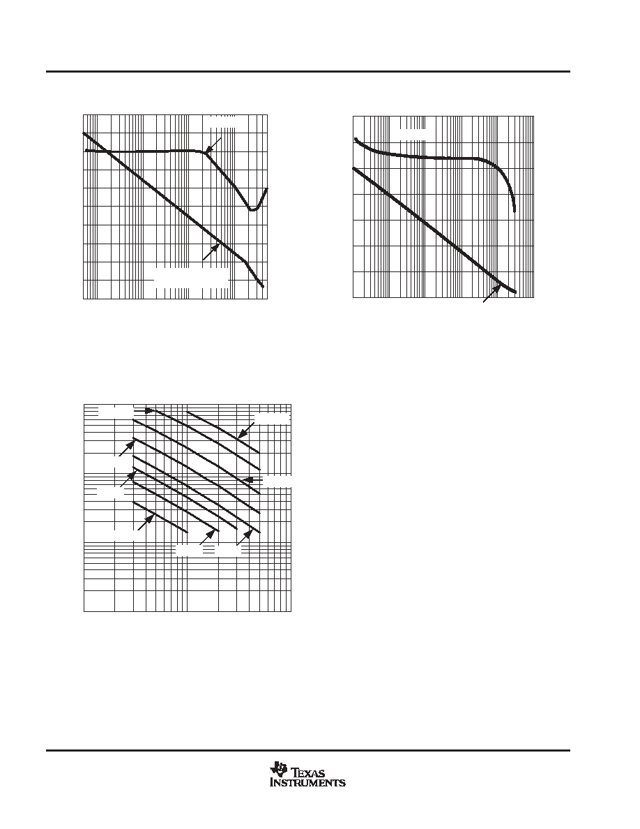
SLUS329A - JUNE 1998 - REVISED AUGUST 2003
10
www.ti.com
10 k
-60
100 k
-40
0
20
60
80
100
120
1 M
10 M
-20
40
140
Figure 5
CURRENT AMPLIFIER GAIN
vs
FREQUENCY
GAIN
fCO = 5.992 MHz
f - Frequency - Hz
Gain - dB
PHASE
-90
-45
-0
Phase -
�
0
-20
40
20
60
80
100
120
100
1000
10 k
100 k
1 M
10 M
Figure 6
VOLTAGE AMPLIFIER GAIN
vs
FREQUENCY
GAIN
PHASE
f - Frequency - Hz
Gain - dB
0
-20
40
20
60
80
100
120
Phase -
�
Figure 7
OSCILLATOR FREQUENCY
vs
LIMIT SET RESISTANCE AND
TIMING CAPACITANCE
RSET - Multiplier Limit Set Resistance - k
f OSC
- Oscillator Frequency - kHz
1
0
10
100
10
100
1 k
10 nF
5 nF
2 nF
3 nF
1 nF
500 pF
200 pF
100 pF

IMPORTANT NOTICE
Texas Instruments Incorporated and its subsidiaries (TI) reserve the right to make corrections, modifications,
enhancements, improvements, and other changes to its products and services at any time and to discontinue
any product or service without notice. Customers should obtain the latest relevant information before placing
orders and should verify that such information is current and complete. All products are sold subject to TI's terms
and conditions of sale supplied at the time of order acknowledgment.
TI warrants performance of its hardware products to the specifications applicable at the time of sale in
accordance with TI's standard warranty. Testing and other quality control techniques are used to the extent TI
deems necessary to support this warranty. Except where mandated by government requirements, testing of all
parameters of each product is not necessarily performed.
TI assumes no liability for applications assistance or customer product design. Customers are responsible for
their products and applications using TI components. To minimize the risks associated with customer products
and applications, customers should provide adequate design and operating safeguards.
TI does not warrant or represent that any license, either express or implied, is granted under any TI patent right,
copyright, mask work right, or other TI intellectual property right relating to any combination, machine, or process
in which TI products or services are used. Information published by TI regarding third-party products or services
does not constitute a license from TI to use such products or services or a warranty or endorsement thereof.
Use of such information may require a license from a third party under the patents or other intellectual property
of the third party, or a license from TI under the patents or other intellectual property of TI.
Reproduction of information in TI data books or data sheets is permissible only if reproduction is without
alteration and is accompanied by all associated warranties, conditions, limitations, and notices. Reproduction
of this information with alteration is an unfair and deceptive business practice. TI is not responsible or liable for
such altered documentation.
Resale of TI products or services with statements different from or beyond the parameters stated by TI for that
product or service voids all express and any implied warranties for the associated TI product or service and
is an unfair and deceptive business practice. TI is not responsible or liable for any such statements.
Following are URLs where you can obtain information on other Texas Instruments products and application
solutions:
Products
Applications
Amplifiers
amplifier.ti.com
Audio
www.ti.com/audio
Data Converters
dataconverter.ti.com
Automotive
www.ti.com/automotive
DSP
dsp.ti.com
Broadband
www.ti.com/broadband
Interface
interface.ti.com
Digital Control
www.ti.com/digitalcontrol
Logic
logic.ti.com
Military
www.ti.com/military
Power Mgmt
power.ti.com
Optical Networking
www.ti.com/opticalnetwork
Microcontrollers
microcontroller.ti.com
Security
www.ti.com/security
Telephony
www.ti.com/telephony
Video & Imaging
www.ti.com/video
Wireless
www.ti.com/wireless
Mailing Address:
Texas Instruments
Post Office Box 655303 Dallas, Texas 75265
Copyright
2003, Texas Instruments Incorporated