
UC1854B
UC2854A, UC2854B
UC3854A, UC3854B
SLUS329B - JUNE 1998 - REVISED FEBRUARY 2005
ADVANCED HIGH POWER FACTOR
PREREGULATOR
1
www.ti.com
FEATURES
D
Controls Boost PWM to Near-Unity Power
Factor
D
Limits Line Current Distortion To < 3%
D
World-Wide Operation Without Switches
D
Accurate Power Limiting
D
Fixed-Frequency Average Current-Mode
Control
D
High Bandwidth (5 MHz), Low-Offset Current
Amplifier
D
Integrated Current- and Voltage Amplifier
Output Clamps
D
Multiplier Improvements: Linearity, 500 mV
V
AC
Offset (Eliminates External Resistor), 0 V
to 5 V Multout Common-Mode Range
D
V
REF
GOOD Comparator
D
Faster and Improved Accuracy ENABLE
Comparator
D
UVLO Options (16 V/10 V or 10.5 V/10 V)
D
300-
�
A Start-Up Supply Current
BLOCK DIAGRAM
DESCRIPTION
The UC3854A/B products are pin compatible
enhanced versions of the UC3854. Like the
UC3854, these products provide all of the
functions necessary for active power factor
corrected preregulators. The controller achieves
near unity power factor by shaping the AC input
line current waveform to correspond to the AC
input line voltage. To do this the UC3854A/B uses
average current mode control. Average current
mode control maintains stable, low distortion
sinusoidal line current without the need for slope
compensation, unlike peak current mode control.
A 1% 7.5 V reference, fixed frequency oscillator,
PWM, voltage amplifier with soft-start, line voltage
feedforward (V
RMS
squarer), input supply voltage
clamp, and over current comparator round out the
list of features.
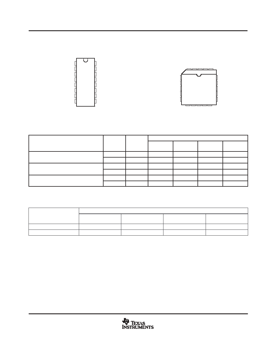
Available in the 16-pin N (PDIP), DW (SOIC-
Wide), and J (CDIP) and 20-pin Q (PLCC)
package. See ordering information on page 3 for
availability by temperature range.
UDG-03110
10
11
6
8
15
1
16
ENA
VSENSE
IAC
VRMS
VCC
GND
GTDRV
2.65 V / 2.15 V
3 V
7
VAO
13
SS
X2
A
B
C
(A) 16 V / 10 V
(B) 10.5 V / 10 V
5
MOUT
4
ISENSE
3
CAO
14
CT
OSC
12
RSET
S
Q
R
R
2
PKLMT
20 V
IC
POWER
7.5 V REF
9
REF
RUN
7.1 V
RUN
VCC
14
�
A
I
MOUT
+
A
B
C
PRODUCTION DATA information is current as of publication date.
Products conform to specifications per the terms of Texas Instruments
standard warranty. Production processing does not necessarily include
testing of all parameters.
Copyright
2003, Texas Instruments Incorporated
UC1854B
UC2854A, UC2854B
UC3854A, UC3854B
SLUS329B - JUNE 1998 - REVISED FEBRUARY 2005
2
www.ti.com
DESCRIPTION (continued)
The UC3854A/B products improve upon the UC3854 by offering a wide bandwidth, low offset current amplifier,
a faster responding and improved accuracy enable comparator, a VREF GOOD comparator, UVLO threshold
options (16 V/10 V for offline, 10.5 V/10 V for startup from an auxiliary 12 V regulator), lower startup supply
current, and an enhanced multiply/divide circuit. New features like the amplifier output clamps, improved
amplifier current sinking capability, and low offset VAC pin reduce the external component count while improving
performance. Improved common mode input range of the multiplier output/current amplifier input allow the
designer greater flexibility in choosing a method for current sensing. Unlike its predecessor, R
SET
controls only
oscillator charging current and has no effect on clamping the maximum multiplier output current. This current
is now clamped to a maximum of 2
�
I
AC
at all times which simplifies the design process and provides foldback
power limiting during brownout and extreme low line conditions.
These devices have limited built-in ESD protection. The leads should be shorted together or the device placed in conductive foam
during storage or handling to prevent electrostatic damage to the MOS gates.
ABSOLUTE MAXIMUM RATINGS
over operating free-air temperature range unless otherwise noted(1)
UCX854A, UCX854B
UNIT
Supply voltage, VCC
22
V
GTDRV current, IGTDRV
Continuous
0.5
A
GTDRV Current, IGTDRV
50% duty cycle
1.5
A
Input voltage
VSENSE, VRMS, ISENSE MOUT
11
V
Input voltage
PKLMT
5
V
Input current
RSET, IAC, PKLMT, ENA
10
mA
Power dissipation
1
W
Junction temperature, TJ
-55 to 150
Storage temperature, Tstg
-65 to 150
�
C
Lead temperature, Tsol, 1,6 mm (1/16 inch) from case for 10 seconds
300
C
(1) Stresses beyond those listed under "absolute maximum ratings" may cause permanent damage to the device. These are stress ratings only,
and functional operation of the device at these or any other conditions beyond those indicated under "recommended operating conditions" is
not implied. Exposure to absolute-maximum-rated conditions for extended periods may affect device reliability. All voltages are with respect to
GND. Currents are positive into and negative out of, the specified terminal. ENA input is internally clamped to approximately 10 V.
RECOMMENDED OPERATING CONDITIONS
MIN
MAX
UNIT
Supply voltage, VCC
10
20
V
UC1854X
-55
125
Operating junction temperature, TJ
UC2854X
-40
85
�
C
Operating junction temperature, TJ
UC3854X
0
70
C
UC1854B
UC2854A, UC2854B
UC3854A, UC3854B
SLUS329B - JUNE 1998 - REVISED FEBRUARY 2005
3
www.ti.com
PACKAGE DESCRIPTION
1
2
3
4
5
6
7
8
16
15
14
13
12
11
10
9
GND
PKLMT
CAO
ISENSE
MOUT
IAC
VAO
VRMS
GTDRV
VCC
CT
SS
RSET
VSENSE
ENA
VREF
J, N and DW PACKAGES
(TOP VIEW)
5
4
6
7
8
18
17
16
15
14
ISENSE
CAOUT
N/C
MOUT
IAC
CT
SS
N/C
RSET
VSENSE
3 2 1 20 19
9 10 11 12 13
PKLMT
GND
N/C
GTDR
V
VCC
VA
O
VRMS
NC
VREF
ENA
Q PACKAGE
(TOP VIEW)
N/C - No connection
ORDERING INFORMATION
UVLO
UVLO
PART NUMBERS
TA
UVLO
TURN-ON
(V)
UVLO
TURN-OFF
(V)
CDIP-16
(J)
PDIP-16
(N)
SOIC-16
(DW)
PLCC-20
(Q)
-55
�
C to 125
�
C
16
10
-
-
-
-
-55
�
C to 125
�
C
10.5
10
UC1854BJ
-
-
-
-40
�
C to 85
�
C
16
10
UC2854AJ
UC2854AN
UC2854ADW
UC2854AQ
-40
�
C to 85
�
C
10.5
10
UC2854BJ
UC2854BN
UC2854BDW
UC2854BQ
0
�
C to 70
�
C
16
10
-
UC3854AN
UC3854ADW
-
0
�
C to 70
�
C
10.5
10
-
UC3854BN
UC3854BDW
-
(1) The DW and Q packages are available taped and reeled. Add TR suffix to device type (e.g. UC2854ADWTR) to order quantities of 2,000
devices per reel for the DW package and 1,000 devices per reel for the Q package.
THERMAL RESISTANCE
PACKAGED DEVICES
RESISTANCES
CDIP-16
(J)
PDIP-16
(N)
SOP-16
(DW)
PLCC-20
(Q)
JC (
�
C/W)
28(2)
45
27
34
JA (
�
C/W)
80-120
90(3)
50-130(3)
43-75(3)
(2)
JC data values stated are derived from MIL-STD-1835B which states "the baseline values shown are worst case (mean +2s) for a 60
�
60
mil microcircuit device silicon die and applicable for devices with die sizes up to 14,400 square mils. For device die sizes greater than
14,400 square mils use the following values, dual-in-line, 11
�
C/W; flat pack and pin grid array, 10
�
C/W.
(3)
JA (junction-to-ambient) applies to devices mounted to five square inch FR4 PC board with one ounce copper where noted. When
resitance range is given, lower values are for five square inch aluminum PC board. Test PWB is 0.062 inches thick and typically uses
0.635 mm trace widths for power packages and 1.3 mm trace widths for non-power packages with a 100
�
100 mil probe land are at the
end of each trace.

UC1854B
UC2854A, UC2854B
UC3854A, UC3854B
SLUS329B - JUNE 1998 - REVISED FEBRUARY 2005
4
www.ti.com
ELECTRICAL CHARACTERISTICS
VCC = 18 V, RT = 8.2 k
, CT = 1.5 nF, VPKLMT = 1 V, VVRMS = 1.5 V, IIAC = 100
�
A, IISENSE = 0 V, VCAO = 3.5 V, VVAO = 5 V, VVSENSE = 3 V,
-40
�
C < TA < 85
�
C for the UC2854A and UC2854B, and 0
�
C < TA <70
�
C for the UC3854A and UC3854B, and TA = TJ (unless otherwise
noted)
PARAMETER
TEST CONDITIONS
MIN
TYP
MAX
UNIT
OVERALL
Supply current, off
CAO = 0 V,
VAO = 0 V,
VCC = VUVLO-0.3 V
250
400
�
A
Supply current, on
12
18
mA
VCC turn-on threshold voltage
UCx854A
15.0
16.0
17.5
VCC turn-on threshold voltage
UCx854B
8.0
10.5
11.2
V
VCC turn-off threshold voltage
9
10
12
V
VCC clamp
IVCC = IVCC(on) + 5 mA
18
20
22
VOLTAGE AMPLIFIER
Input voltage
2.9
3.0
3.1
V
VSENSE bias current
-500
-25
500
nA
Open loop gain
2 V
VOUT
5 V
70
100
dB
VOH
High-level output voltage
ILOAD = -500
�
A
6
V
VOL
Low-level output voltage
ILOAD = 500
�
A
0.3
0.5
V
ISC
Output short-circuit current
VOUT = 0 V
1.5
3.5
mA
Gain bandwidth product(1)
fIN = 100 kHz,
10 mVP-P
1
MHz
CURRENT AMPLIFIER
Input offset voltage
VCM = 0 V,
TA = 25
�
C
-4
0
mV
Input offset voltage
VCM = 0 V,
overtemperature
-5.5
0
mV
Input bias current, ISENSE
VCM = 0 V
-500
500
nA
Open loop gain
2 V
VOUT
6 V
80
110
dB
VOH
High-level output voltage
ILOAD = -500
�
A
8
V
VOL
Low-level output voltage
ILOAD = 500
�
A
0.3
0.5
V
ISC
Output short-circuit current
VOUT = 0 V
1.5
3.5
mA
CMRR
Common mode rejection range
-0.3
5.0
V
Gain bandwidth product(1)
fIN = 100 kHz,
10 mVP-P
3
5
MHz
REFERENCE
Output voltage
IREF = 0 mA,
TA = 25
�
C
7.4
7.5
7.6
V
Output voltage
IREF = 0 mA
7.35
7.50
7.65
V
Load regulation
1 mA
IREF
10 mA
0
8
20
mV
Line regulation
12 V
VCC
18 V
0
14
25
mV
ISC
Short circuit current
VREF = 0 V
25
35
60
mA
(1) Ensured by design. Not production tested.
(2) Gain constant. (K)
+
I
IAC
V
VAO
*
1.5 V
V
VRMS
2
I
MOUT
UC1854B
UC2854A, UC2854B
UC3854A, UC3854B
SLUS329B - JUNE 1998 - REVISED FEBRUARY 2005
5
www.ti.com
ELECTRICAL CHARACTERISTICS
VCC = 18 V, RT = 8.2 k
, CT = 1.5 nF, VPKLMT = 1 V, VVRMS = 1.5 V, IIAC = 100
�
A, IISENSE = 0 V, VCAO = 3.5 V, VVAO = 5 V, VVSENSE = 3 V,
-40
�
C < TA < 85
�
C for the UC2854A and UC2854B, and 0
�
C < TA <70
�
C for the UC3854A and UC3854B, and TA = TJ (unless otherwise
noted)
PARAMETER
TEST CONDITIONS
MIN
TYP
MAX
UNIT
OSCILLATOR
Initial accuracy
TA = 25
�
C
85
100
115
kHz
Voltage stability
12 V
VCC
18 V
1%
Total variation
Line, temperature
80
120
kHz
Ramp amplitude (peak-to-peak)
4.9
5.9
V
Ramp valley voltage
0.8
1.3
V
ENABLE/SOFT-START/CURRENT LIMIT
Enable threshold voltage
2.35
2.55
2.80
V
Enable hysteresis
VFAULT = 2.5 V
500
600
mV
Enable input bias current
VENA = 0 V
-2
-5
�
A
Propagation delay to disable time(1)
Enable overdrive = 100 mV
300
ns
Soft-start charge current
VSS = 2.5 V
10
14
24
Peak limit offset voltage
-15
15
mV
Peak limit input current
VPKLMT = -0.1 V
-200
-100
�
A
Peak limit propagation delay time(1)
150
ns
MULTIPLIER
Output current, IAC limited
IAC = 100
�
A,
VRMS = 1 V,
RSET = 10 k
-220
-200
-170
A
Output current, zero
IAC = 0
�
A,
RSET = 10 k
-2.0
-0.2
2.0
�
A
Output current, power limited
VRMS = 1.5 V,
Va = 6 V
-230
-200
-170
VRMS = 1.5 V,
Va = 2 V
-22
�
A
Output current
VRMS = 1.5 V,
Va = 5 V
-156
Output current
VRMS = 5 V,
Va = 2 V
-2
�
A
VRMS = 5 V,
Va = 5 V
-14
�
A
Gain constant(2)
VRMS = 1.5 V, Va = 6V, TA = 25
�
C
-1.1
-1.0
-0.9
A/A
GATE DRIVER
VOH
High-level output voltage
IOUT = -200 mA,
VCC = 15 V
12.0
12.8
V
VOL
Low-level output voltage
IOUT = 200 mA
1.0
2.2
V
IOUT = 10 mA
300
500
mV
Low-level UVLO voltage
IOUT = 50 mA,
VCC = 0 V
0.9
1.5
V
Output rise time(1)
CLOAD = 1 nF
35
ns
Output fall time(1)
CLOAD = 1 nF
35
ns
Output peak current(1)
CLOAD = 10 nF
1.0
A
(1) Ensured by design. Not production tested.
(2) Gain constant. (K)
+
I
IAC
V
VAO
*
1.5 V
V
VRMS
2
I
MOUT