 | –≠–ª–µ–∫—Ç—Ä–æ–Ω–Ω—ã–π –∫–æ–º–ø–æ–Ω–µ–Ω—Ç: UC2855AN | –°–∫–∞—á–∞—Ç—å:  PDF PDF  ZIP ZIP |
Document Outline
- Application Notes
- Design Notes
UC1855A/B
UC2855A/B
UC3855A/B
DESCRIPTION
The UC1855A/B provides all the control features necessary for high
power, high frequency PFC boost converters. The average current mode
control method allows for stable, low distortion AC line current program-
ming without the need for slope compensation. In addition, the UC1855
utilizes an active snubbing or ZVT (Zero Voltage Transition technique) to
dramatically reduce diode recovery and MOSFET turn-on losses, result-
ing in lower EMI emissions and higher efficiency. Boost converter switch-
ing frequencies up to 500kHz are now realizable, requiring only an
additional small MOSFET, diode, and inductor to resonantly soft switch
the boost diode and switch. Average current sensing can be employed us-
ing a simple resistive shunt or a current sense transformer. Using the cur-
rent sense transformer method, the internal current synthesizer circuit
buffers the inductor current during the switch on-time, and reconstructs the
inductor current during the switch off-time. Improved signal to noise ratio
and negligible current sensing losses make this an attractive solution for
higher power applications.
The UC1855A/B also features a single quadrant multiplier, squarer, and
divider circuit which provides the programming signal for the current loop.
The internal multiplier current limit reduces output power during low line
conditions. An overvoltage protection circuit disables both controller out-
puts in the event of a boost output OV condition.
Low startup supply current, UVLO with hysteresis, a 1% 7.5V reference,
voltage amplifier with softstart, input supply voltage clamp, enable com-
parator, and overcurrent comparator complete the list of features. Avail-
able packages include: 20 pin N, DW, Q, J, and L.
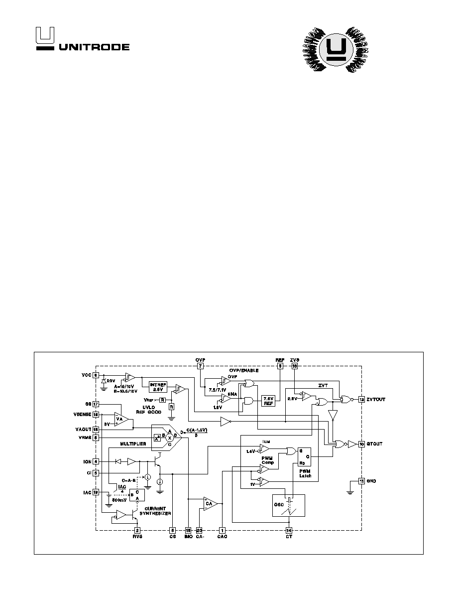
BLOCK DIAGRAM
High Performance Power Factor Preregulator
FEATURES
∑
Controls Boost PWM to Near Unity
Power Factor
∑
Fixed Frequency Average Current
Mode Control Minimizes Line Current
Distortion
∑
Built-in Active Snubber (ZVT) allows
Operation to 500kHz, improved EMI
and Efficiency
∑
Inductor Current Synthesizer allows
Single Current Transformer Current
Sense for Improved Efficiency and
Noise Margin
∑
Accurate Analog Multiplier with Line
Compensator allows for Universal
Input Voltage Operation
∑
High Bandwidth (5MHz), Low Offset
Current Amplifier
∑
Overvoltage and Overcurrent
protection
∑
Two UVLO Threshold Options
∑
150
µ
A Startup Supply Current Typical
∑
Precision 1% 7.5V Reference
6/98
License Patent from Pioneer Magnetics. Pin numbers refer to DIL-20 J or N packages.
UDG-94001-2
2
UC1855A/B
UC2855A/B
UC3855A/B
ABSOLUTE MAXIMUM RATINGS
Supply Voltage VCC
. . . . . . . . . . . . . . . . . . . . . . . . . .
Internally Limited
VCC Supply Clamp Current . . . . . . . . . . . . . . . . . . . . . . . 20mA
PFC Gate Driver Current (continuous) . . . . . . . . . . . . . . ± 0.5A
PFC Gate Driver Current (peak) . . . . . . . . . . . . . . . . . . . ± 1.5A
ZVT Drive Current (continuous
)
. . . . . . . . . . . . . . . . . . . ± 0.25A
ZVT Drive Current (peak
)
. . . . . . . . . . . . . . . . . . . . . . . ± 0.75A
I
nput Current (IAC, R
T
, RVA) . . . . . . . . . . . . . . . . . . . . . . . 5mA
Analog Inputs (except Peak Limit) . . . . . . . . . . . . . .
-
0.3 to 10V
Peak Limit Input . . . . . . . . . . . . . . . . . . . . . . . . . . .
-
0.3 to 6.5V
Softstart Sinking Current . . . . . . . . . . . . . . . . . . . . . . . . . 1.5mA
Storage Temperature . . . . . . . . . . . . . . . . . . .
-
65∞C to +150
∞
C
Junction Temperature . . . . . . . . . . . . . . . . . . .
-
55∞C to +150
∞
C
Lead Temperature (Soldering, 10 sec.) . . . . . . . . . . . . . +300
∞
C
Currents are positive into, negative out of the specified termi-
nal. Consult Packaging Section of Databook for thermal limita-
tions and considerations of packages. All voltages are
referenced to GND.
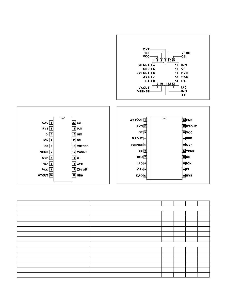
CONNECTION DIAGRAMS
PLCC-20 & LCC-20 (Top View)
Q or L Package
DIL≠20 (Top View)
J or N Package
SOIC-20 (Top View)
DW Package
ELECTRICAL CHARACTERISTICS:
Unless otherwise specified: VCC = 18V, R
T
= 15k, RVS = 23k, CT = 470pF, CI =
150pF
,
VRMS = 1.5V, IAC = 100
µ
A, I
SENSE
= 0V, CA
OUT
= 4V, VAOUT= 3.5V, VSENSE = 3V. T
A
= T
J.
T
A
= ≠55
∞
C to 125∞C
(UC1855A/B)
,
≠40
∞
C to 85∞C (UC2855A/B), 0
∞
C to 70
∞
C (UC3855A/B).
PARAMETER
TEST CONDITIONS
MIN
TYP
MAX
UNITS
Overall
Supply Current, OFF
CAO, VAOUT = 0V, VCC = UVLO
-
0.3V
150
500
µ
A
Supply Current, OPERATING
17
25
mA
VCC Turn-On Threshold
UC1855A
15.5
17.5
V
VCCTurn-Off Threshold
UC1855A,B
9
10
V
VCC Turn-On Threshold
UC1855B
10.5
10.8
V
VCC Clamp
I(VCC) = I
CC(on)
+ 5mA
18
20
22
V
Voltage Amplifier
Input Voltage
2.9
3.1
V
VSENSE Bias Current
-
500
25
500
nA
Open Loop Gain
V
OUT
= 2 to 5V
65
80
dB
V
OUT
High
I
LOAD
= ≠300
µ
A
5.75
6
6.25
V
V
OUT
Low
I
LOAD
= 300
µ
A
0.3
0.5
V
Output Short Circuit Current
V
OUT
= 0V
0.6
3
mA
3
UC1855A/B
UC2855A/B
UC3855A/B
ELECTRICAL CHARACTERISTICS:
Unless otherwise specified: VCC = 18V, R
T
= 15k, RVS = 23k, CT = 470pF, CI =
150pF
,
VRMS = 1.5V, IAC = 100
µ
A, I
SENSE
= 0V, CA
OUT
= 4V, VAOUT= 3.5V, VSENSE = 3V. T
A
= T
J.
T
A
= ≠55
∞
C to 125∞C
(UC1855A/B)
,
≠40
∞
C to 85∞C (UC2855A/B), 0
∞
C to 70
∞
C (UC3855A/B).
PARAMETER
TEST CONDITIONS
MIN
TYP
MAX
UNITS
Current Amplifier
Input Offset Voltage
V
CM
=
-
2.5V
-
4
4
mV
Input Bias Current (Sense)
V
CM
= 2.5V
-
500
500
nA
Open Loop Gain
V
CM
= 2.5V, V
OUT
= 2 to 6V
80
110
dB
V
OUT
High
I
LOAD
=
-
500
µ
A
6
V
V
OUT
Low
I
LOAD
= 500
µ
A
0.3
0.5
V
Output Short Circuit Current
V
OUT
= 0V
1
3
mA
Common Mode Range
-
0.3
5
V
Gain Bandwidth Product
F
IN
= 100kHz, 10mV, P≠P, T
A
= 25∞C
2.5
5
MHz
Reference
Output Voltage
I
REF
= 0mA, T
A
= 25∞C
7.388
7.5
7.613
V
I
REF
= 0mA
7.313
7.5
7.688
V
Load Regulation
I
REF
= 1 to 10 mA
-
15
15
mV
Line Regulation
VCC = 15 to 35V
-
10
10
mV
Short Circuit Current
REF = 0V
20
45
65
mA
Oscillator
Initial Accuracy
T
A
= 25
∞
C
170
200
230
kHz
Voltage Stability
V
CC
= 12 to 18V
1
%
Total Variation
Line, Temp.
160
240
kHz
Ramp Amplitude (P≠P)
4.9
5.9
V
Ramp Valley Voltage
1.1
1.6
V
Enable/OVP/Current Limit
Enable Threshold
1.8
2.2
V
OVP Threshold
7.5
7.66
V
OVP Hysteresis
200
400
600
mV
OVP Propagation Delay
200
ns
OVP Input Bias Current
V= 7.5V
1
10
µ
A
PK
LIMIT
Threshold
1.25
1.5
1.75
V
PK
LIMIT
Input Current
V
PKLIMIT
= 1.5V
100
µ
A
PK
LIMIT
Prop. Delay
100
ns
Multiplier
Output Current - IAC Limited
IAC = 100
µ
A, VRMS = 1V
-
235
-
205
-
175
µ
A
Output Current - Zero
IAC = 0
µ
A
-
2
-
0.2
2
µ
A
Output Current - Power Limited
VRMS = 1.5V, VAOUT = 5.5V
-
250
-
209
-
160
µ
A
Output Current
VRMS = 1.5V, VAOUT = 2V
-
26
µ
A
VRMS = 1.5V VAOUT = 5V
-
190
µ
A
VRMS = 5V, VAOUT = 2V
-
3
µ
A
VRMS = 5V, VAOUT = 5V
-
17
µ
A
Gain Constant
Refer to Note 1
-
0.95
-
0.85
-
0.75
1/V
Gate Driver Output
Output High Voltage
l
OUT
=
-
200mA, VCC = 15V
12
12.8
V
Output Low Voltage
l
OUT
= 200mA
1
2.2
V
Output Low Voltage
l
OUT
= 10mA
300
500
mV
Output Low (UVLO)
l
OUT
= 50mA, VCC = 0V
0.9
1.5
V
Output RISE/FALL Time
C
LOAD
= 1nF
35
ns
Output Peak Current
C
LOAD
= 10nF
1.5
A

4
UC1855A/B
UC2855A/B
UC3855A/B
ELECTRICAL CHARACTERISTICS:
Unless otherwise specified: VCC = 18V, R
T
= 15k, RVS = 23k, CT = 470pF, CI =
150pF
,
VRMS = 1.5V, IAC = 100
µ
A, I
SENSE
= 0V, CA
OUT
= 4V, VAOUT= 3.5V, VSENSE = 3V. T
A
= T
J.
T
A
= ≠55
∞
C to 125∞C
(UC1855A/B)
,
≠40
∞
C to 85∞C (UC2855A/B), 0
∞
C to 70
∞
C (UC3855A/B).
PARAMETER
TEST CONDITIONS
MIN
TYP
MAX
UNITS
ZVT
Reset Threshold
2.3
2.6
2.9
V
Input Bias Current
V = 2.5V, V
CT
= 0
6
20
µ
A
Propagation Delay
Measured at ZVTOUT
100
ns
Maximum Pulse Width
400
ns
Output High Voltage
l
OUT
=
-
100mA, V
CC
= 15V
12
12.8
V
Output Low Voltage
l
OUT
= 100mA
1
2.2
V
l
OUT
= 10mA
300
900
mV
Output Low (UVLO)
l
OUT
= 50mA, V
CC
= 0V
0.9
1.5
V
Output RISE/FALL Time
C
LOAD
= 1nF
35
ns
Output Peak Current
C
LOAD
= 10nF
0.75
A
Current Synthesizer
I
ON
to CS Offset
VION = 0V
30
50
mV
Cl Discharge Current
IAC = 50
µ
A
105
118
140
µ
A
IAC = 500
µ
A
5
µ
A
IAC Offset Voltage
0.3
0.65
1.1
V
ION Buffer Slew Rate
10
V/
µ
s
ION Input Bias Current
V
ION
= 2V
2
15
µ
A
RVS Output Voltage
23k from RVS to GND
2.87
3
3.13
V
Note 1: Gain constant (K) =
IAC VA
V
V
IMO
OUT
RMS
∑
∑
(
. )
(
)
1 5
at V
RMS
= 1.5V, VA
OUT
= 5.5V.
PIN DESCRIPTIONS
CA
-:
This is the inverting input to the current amplifier.
Connect the required compensation components be-
tween this pin and CAOUT. The common mode operating
range for this input is between
-
0.3V and 5V.
CAO
:
This is the output of the wide bandwidth current
amplifier and one of the inputs to the PWM duty cycle
comparator. The output signal generated by this amplifier
commands the PWM to force the correct input current.
The output can swing from 0.1V to 7.5V.
CI
:
The level shifted current sense signal is impressed
upon a capacitor connected between this pin and GND.
The buffered current sense transformer signal charges
the capacitor when the boost switch is on. When the
switch is off, the current synthesizer discharges the ca-
pacitor at a rate proportional to the dI/dt of the boost in-
ductor current. In this way, the discharge current is
approximately equal to
3
4
V
RRVS
IAC
≠
.
Discharging the CI capacitor in this fashion, a "recon-
structed" version of the inductor current is generated us-
ing only one current sense transformer.
CS: The reconstructed inductor current waveform gener-
ated on the CI pin is level shifted down a diode drop to
this pin. Connect the current amplifier input resistor be-
tween CS and the inverting input of the current amplifier.
The waveform on this pin is compared to the multiplier
output waveform through the average current sensing
current amplifier. The input to the peak current limiting
comparator is also connected to this pin. A voltage level
greater than 1.5 volts on this pin will trip the comparator
and disable the gate driver output.
CT: A capacitor from CT to GND sets the PWM oscillator
frequency according to the following equation:
f
CT
∑
1
11200
.
Use a high quality ceramic capacitor with low ESL and
ESR for best results. A minimum CT value of 200pF in-
sures good accuracy and less susceptibility to circuit lay-
out parasitics. The oscillator and PWM are designed to
provide practical operation to 500kHz.
GND: All voltages are measured with respect to this pin.
All bypass and timing capacitors connected to GND
should have leads as short and direct as possible.

5
UC1855A/B
UC2855A/B
UC3855A/B
GTOUT: The output of the PWM is a 1.5A peak totem
pole MOSFET gate driver on GTOUT. A series resistor
between GTOUT and the MOSFET gate of at least 10
ohms should be used to limit the overshoot on GTOUT.
In addition, a low V
F
Schottky diode should be connected
between GTOUT and GND to limit undershoot and possi-
ble erratic operation.
IAC: This is a current input to the multiplier. The current
into this pin should correspond to the instantaneous
value of the rectified AC input line voltage. This is accom-
plished by connecting a resistor directly between IAC and
the rectified input line voltage. The nominal 650mV level
present on IAC negates the need for any additional com-
pensating resistors to accommodate for the zero cross-
ings of the line. A current equal to one fourth of the IAC
current forms one of the inductor current synthesizer in-
puts.
IMO: This is the output of the multiplier, and the non-
inverting input of the current amplifier. Since this output is
a current, connect a resistor between this pin and ground
equal in value to the input resistor of the current amplifier.
The common mode operating range for this pin is
-
0.3V
to 5V.
ION: This pin is the current sensing input. It should be
connected to the secondary side output of a current
sensing transformer whose primary winding is in series
with the boost switch. The resultant signal applied to this
input is buffered and level shifted up a diode to the CI ca-
pacitor on the CI pin. The ION buffer has a source only
output. Discharge of the CI cap is enabled through the
current synthesizer circuitry. The current sense trans-
former termination resistor should be designed to obtain
a 1V input signal amplitude at peak switch current.
OVP: This pin senses the boost output voltage through a
voltage divider. The enable comparator input is TTL com-
patible and can be used as a remote shutdown port. A
voltage level below 1.8V, disables V
REF
, oscillator, and
the PWM circuitry via the enable comparator. Between
1.8V and V
REF
(7.5V) the UC1855 is enabled. Voltage
levels above 7.5V will set the PWM latch via the hystere-
tic OVP comparator and disable both ZVTOUT and
GTOUT until the OVP level has decayed by the nominal
hysteresis of 400mV. If the voltage divider is designed to
initiate an OVP fault at 5% of OV, the internal hysteresis
enables normal operation again when the output voltage
has reached its nominal regulation level. Both the OVP
and enable comparators have direct logical connections
to the PWM output and exhibit typical propagation delays
of 200ns.
REF
:
REF is the output of the precision reference. The
output is capable of supplying 25mA to peripheral cir-
cuitry and is internally short circuit current limited. REF is
disabled and low whenever VCC is below the UVLO
threshold, and when OVP is below 1.8V. A REF "GOOD"
comparator senses REF and disables the stage until
REF has attained approximately 90% of its nominal
value. Bypass REF to GND with a 0.1
µ
F or larger ce-
ramic capacitor for best stability.
RVS: The nominal 3V signal present on the VSENSE pin
is buffered and brought out to the RVS pin. A current pro-
portional to the output voltage is generated by connect-
ing a resistor between this pin and GND. This current
forms the second input to the current synthesizer.
VAO: This is the output of the voltage amplifier. At a
given input RMS voltage, the voltage on this pin will vary
directly with the output load. The output swing is limited
from approximately 100mV to 6V. Voltage levels below
1.5V on this pin will inhibit the multiplier output.
VCC: Positive supply rail for the IC. Bypass this pin to
GND with a 1
µ
F low ESL, ESR ceramic capacitor. This
pin is internally clamped to 20V. Current into this clamp
should be limited to less than 10mA. The UC1855A has a
15.5V (nominal) turn on threshold with 6 volts of hystere-
sis while the UC1855B turns on at 10.5V with 500mV of
hysteresis.
VRMS: This pin is the feedforward line voltage compen-
sation input to the multiplier. A voltage on VRMS propor-
tional to the AC input RMS voltage commands the
multiplier to alter the current command signal by
1/VRMS
2
to maintain a constant power balance. The in-
put to VRMS is generally derived from a two pole low
pass filter/voltage divider connected to the rectified AC
input voltage. This feature allows universal input supply
voltage operation and faster response to input line fluc-
tuations for the PFC boost preregulator. For most de-
signs, a voltage level of 1.5V on this pin should
correspond to low line, and 4.7V for high line. The input
range for this pin extends from 0 to 5.5V.
VSENSE: This pin is the inverting input of the voltage
amplifier and serves as the output voltage feedback point
for the PFC boost converter. It senses the output voltage
through a voltage divider which produces a nominal 3V.
The voltage loop compensation is normally connected
between this pin and VAO. The VSENSE pin must be
above 1.5V at 25∞C, (1.9V at ≠55∞C) for the current syn-
thesizer to work properly.
PIN DESCRIPTIONS (cont.)
6
UC1855A/B
UC2855A/B
UC3855A/B
ZVS: This pin senses when the drain voltage of the main
MOSFET switch has reached approximately zero volts,
and resets the ZVT latch via the ZVT comparator. A mini-
mum and maximum ZVTOUT pulse width are program-
mable from this pin. To directly sense the
400V drain
voltage of the main switch, a blocking diode is connected
between ZVS and the high voltage drain. When the drain
reaches 0V, the level on ZVS is
0.7V which is below the
2.6V ZVT comparator threshold. The maximum ZVTOUT
pulse width is approximately equal to the oscillator blank-
ing period time.
ZVTOUT: The output of the ZVT block is a 750mA peak
totem pole MOSFET gate driver on ZVTOUT. Since the
ZVT MOSFET switch is typically 3X smaller than the
main switch, less peak current is required from this out-
put. Like GTOUT, a series gate resistor and Schottky di-
ode to GND are recommended. This pin may also be
used as a high current synchronization output driver.
PIN DESCRIPTIONS (cont.)
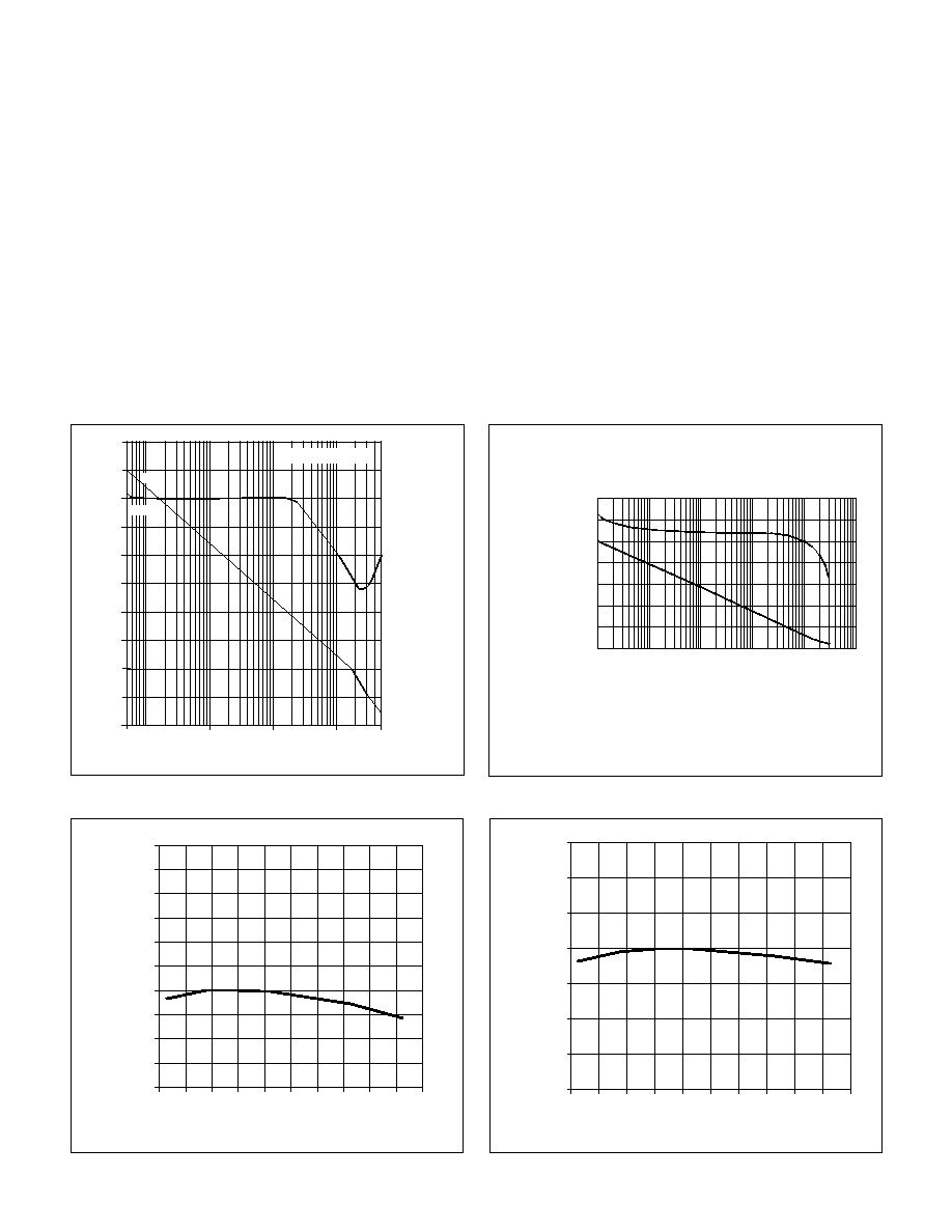
log f
Gain (dB)
-60
-40
-20
0
20
40
60
0
80
-45
Phase
Degrees
100
-90
120
10kHz
1MHz
10MHz
100kHz
Gain
Phase
5.992 496 516 MHz
Figure 1. Current Amplifier Frequency Response
Frequency
kHz
Phase
Margin
degrees
Open-Loop
Gain
dB
-20
0
20
40
60
80
100
120
0.1
1
10
100
1000
10000
Figure 2. Voltage Amplifier Gain Phase vs Frequency
10
12
14
16
18
20
22
24
-60 -40 -20
0
20 40 60 80 100 120 140
TEMPERATURE ∞C
mA
Figure 4. Supply Current ON
2.90
2.92
2.94
2.96
2.98
3.00
3.02
3.04
3.06
3.08
3.10
-60 -40 -20 0
20 40 60 80 100 120 140
TEMPERATURE ∞C
VOL
T
S
Figure 3. Voltage Amplifier Input Threshold
For more information see Unitrode Applications Note U-153.
7
UC1855A/B
UC2855A/B
UC3855A/B
-0.95
-0.93
-0.91
-0.89
-0.87
-0.85
-0.83
-0.81
-0.79
-0.77
-0.75
-60 -40 -20 0
20 40 60 80 100 120 140
TEMPERATURE ∞C
GAI
N
CONST
A
NT
(K)
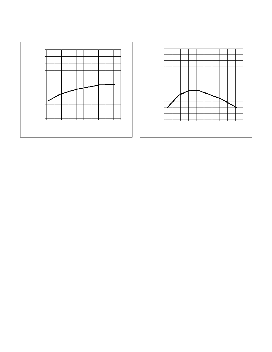
Figure 5. Multiplier Current Gain Constant
170
175
180
185
190
195
200
205
210
215
220
225
230
-60 -40 -20 0
20 40 60 80 100 120 140
TEMPERATURE ∞C
kH
z
Figure 6. Oscillator Initial Accuracy

8
UC1855A/B
UC2855A/B
UC3855A/B
Figure 7. Typical Application
TYPICAL APPLICATION
UDG-95165-1
UNITRODE CORPORATION
7 CONTINENTAL BLVD. ∑ MERRIMACK, NH 03054
TEL. (603) 424-2410 FAX (603) 424-3460

IMPORTANT NOTICE
Texas Instruments and its subsidiaries (TI) reserve the right to make changes to their products or to discontinue
any product or service without notice, and advise customers to obtain the latest version of relevant information
to verify, before placing orders, that information being relied on is current and complete. All products are sold
subject to the terms and conditions of sale supplied at the time of order acknowledgement, including those
pertaining to warranty, patent infringement, and limitation of liability.
TI warrants performance of its semiconductor products to the specifications applicable at the time of sale in
accordance with TI's standard warranty. Testing and other quality control techniques are utilized to the extent
TI deems necessary to support this warranty. Specific testing of all parameters of each device is not necessarily
performed, except those mandated by government requirements.
CERTAIN APPLICATIONS USING SEMICONDUCTOR PRODUCTS MAY INVOLVE POTENTIAL RISKS OF
DEATH, PERSONAL INJURY, OR SEVERE PROPERTY OR ENVIRONMENTAL DAMAGE ("CRITICAL
APPLICATIONS"). TI SEMICONDUCTOR PRODUCTS ARE NOT DESIGNED, AUTHORIZED, OR
WARRANTED TO BE SUITABLE FOR USE IN LIFE-SUPPORT DEVICES OR SYSTEMS OR OTHER
CRITICAL APPLICATIONS. INCLUSION OF TI PRODUCTS IN SUCH APPLICATIONS IS UNDERSTOOD TO
BE FULLY AT THE CUSTOMER'S RISK.
In order to minimize risks associated with the customer's applications, adequate design and operating
safeguards must be provided by the customer to minimize inherent or procedural hazards.
TI assumes no liability for applications assistance or customer product design. TI does not warrant or represent
that any license, either express or implied, is granted under any patent right, copyright, mask work right, or other
intellectual property right of TI covering or relating to any combination, machine, or process in which such
semiconductor products or services might be or are used. TI's publication of information regarding any third
party's products or services does not constitute TI's approval, warranty or endorsement thereof.
Copyright
©
1999, Texas Instruments Incorporated