 | –≠–ª–µ–∫—Ç—Ä–æ–Ω–Ω—ã–π –∫–æ–º–ø–æ–Ω–µ–Ω—Ç: UC285-ADJ | –°–∫–∞—á–∞—Ç—å:  PDF PDF  ZIP ZIP |
UC285 1, UC285 2, UC285 3, UC285 ADJ, UC385 1, UC385 2, UC385 3, UC385 ADJ
FAST TRANSIENT RESPONSE 5 A
LOW DROPOUT REGULATOR
SLUS212E - NOVEMBER 1999 - REVISED FEBRUARY 2004
1
POST OFFICE BOX 655303
∑
DALLAS, TEXAS 75265
D
Fast Transient Response
D
10-mA to 5-A Load Current
D
Short Circuit Protection
D
Maximum Dropout of 500-mV at 5-A Load
Current
D
Separate Bias (VB) and VIN Pins
D
Available in Adjustable or Fixed Output
Voltages
D
5-Pin Package Allows Kelvin Sensing of
Load Voltage
D
Reverse Current Protection
description
The UC385 is a low dropout linear regulator providing a quick response to fast load changes. Combined with
its precision onboard reference, the UC385 excels at driving GTL and BTL buses. Due to its fast response to
load transients, the total capacitance required to decouple the regulator's output can be significantly decreased
when compared to standard LDO linear regulators.
Dropout voltage (VIN to VOUT) is only 490 mV maximum and 350 mV typical at 5-A load (0
∞
C to 100
∞
C).
The onboard bandgap reference is stable with temperature and scaled for a 1.2 V input to the internal power
amplifier. The UC385 is available in fixed output voltages of 1.5 V, 2.1 V, or 2.5 V. The output voltage of the
adjustable version can be set with two external resistors. If the external resistors are omitted, the output voltage
defaults to 1.2 V.
block diagram
+
THERMAL
SHUTDOWN
1.2 V
BANDGAP
REFERENCE
R2
R1
3
5
SHORT
CIRCUIT
SENSE
2
1
4
UC382-ADJ
UC382-1 (1.5 V)
UC382-2 (2.1 V)
UC382-3 (2.5 V)
OPEN
0
2 k
500
2 k
1.5 k
2 k
2.16 k
R1
R2
ADJ
GND
VOUT
VIN
VB
UDG-00084
Copyright
1998-2004, Texas Instruments Incorporated
PRODUCTION DATA information is current as of publication date.
Products conform to specifications per the terms of Texas Instruments
standard warranty. Production processing does not necessarily include
testing of all parameters.
Please be aware that an important notice concerning availability, standard warranty, and use in critical applications of
Texas Instruments semiconductor products and disclaimers thereto appears at the end of this data sheet.
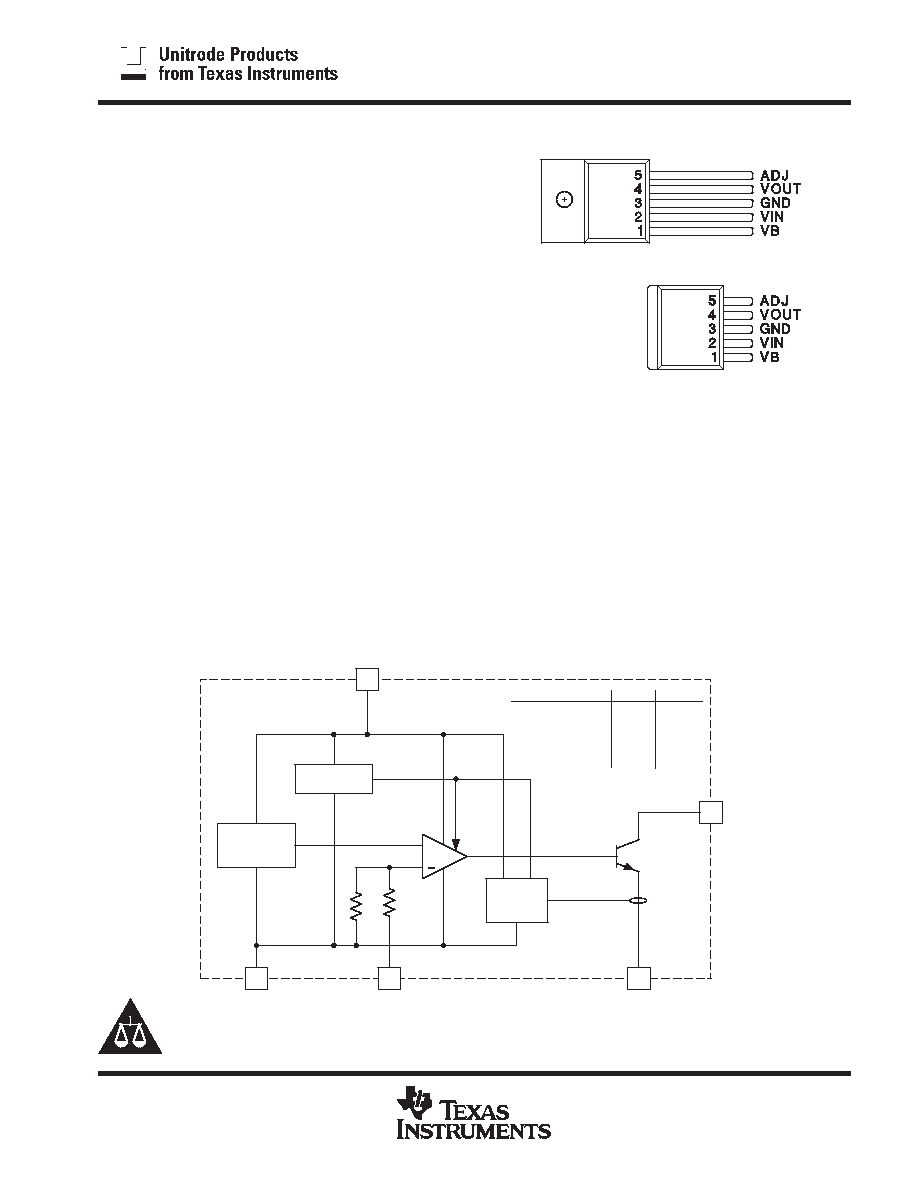
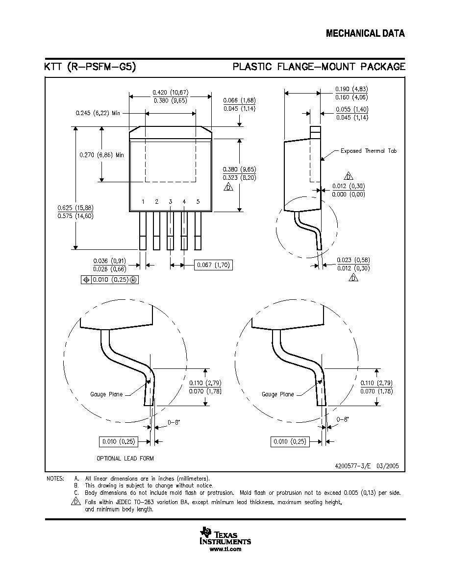
5-PIN TO-263
TD PACKAGE
(TOP VIEW)
5-PIN TO-220
T PACKAGE (TOP VIEW)
Note: Tab = Ground
All trademarks are the property of their respective owners.
UC285 1, UC285 2, UC285 3, UC285 ADJ, UC385 1, UC385 2, UC385 3, UC385 ADJ
FAST TRANSIENT RESPONSE 5 A
LOW DROPOUT REGULATOR
SLUS212E - NOVEMBER 1999 - REVISED FEBRUARY 2004
2
POST OFFICE BOX 655303
∑
DALLAS, TEXAS 75265
absolute maximum ratings over operating free-air temperature (unless otherwise noted)
VIN
7.5 V
. . . . . . . . . . . . . . . . . . . . . . . . . . . . . . . . . . . . . . . . . . . . . . . . . . . . . . . . . . . . . . . . . . . . . . . . . . . . . . . . . . . . .
Output voltage
1.2 V to -6.0 V
. . . . . . . . . . . . . . . . . . . . . . . . . . . . . . . . . . . . . . . . . . . . . . . . . . . . . . . . . . . . . . . . . . . .
Storage temperature
-65
∞
C to 150
∞
C
. . . . . . . . . . . . . . . . . . . . . . . . . . . . . . . . . . . . . . . . . . . . . . . . . . . . . . . . . . . . .
Junction temperature
-55
∞
C to 150
∞
C
. . . . . . . . . . . . . . . . . . . . . . . . . . . . . . . . . . . . . . . . . . . . . . . . . . . . . . . . . . . . .
Lead temperature (soldering, 10 seconds)
300
∞
C
. . . . . . . . . . . . . . . . . . . . . . . . . . . . . . . . . . . . . . . . . . . . . . . . . .
Stresses beyond those listed under "absolute maximum ratings" may cause permanent damage to the device. These are stress ratings only, and
functional operation of the device at these or any other conditions beyond those indicated under "recommended operating conditions" is not
implied. Exposure to absolute-maximum-rated conditions for extended periods may affect device reliability.
AVAILABLE OPTIONS(1)
PACKAGED DEVICES
TJ
TO-220 (T)
TO-263 (TD)(2)
TJ
OUTPUT VOLTAGE
OUTPUT VOLTAGE
1.5 V
2.1 V
2.5 V
1.2 V or ADJ
1.5 V
2.1 V
2.5 V
1.2 V or ADJ
≠40
∞
C to 100
∞
C
285T-1
285T-2
285T-3
285T-ADJ
285TD-1
285TD-2
285TD-3
285TD-ADJ
0
∞
C to 100
∞
C
385T-1
385T-2
385T-3
385T-ADJ
385TD-1
385TD-2
385TD-3
385TD-ADJ
1. For more package and ordering information, see the Package Option Addendum located at the end of this data sheet.
2. For 50 piece reel, add KTTT (e.g., UC285TDKTTT-1); for 500 piece reel, add TR (e.g., UC285TDTR-1).
electrical characteristics unless otherwise stated, these parameters apply for T
A
= -40
∞
C to 100
∞
C
for the UC285-x series and 0
∞
C to 100
∞
C for the UC385-x, VB = 5 V; VIN = 3.3 V, VOUT = 2.5 V, T
A
= T
J
.
PARAMETER
TEST CONDITION
MIN
TYP
MAX
UNIT
UC385-3 Fixed 2.5 V, 5-A Family
Output voltage
UC385-3
IVOUT = 100 mA
2.475
2.5
2.525
V
Output voltage
UC285-3
IVOUT = 100 mA
2.45
2.5
2.525
V
Load regulation
IVOUT = 10 mA to 5 A
0.5
4
mV
VIN PSRR
80
110
dB
VB PSRR
50
65
dB
VIN dropout voltage (VIN - VOUT)
IVOUT = 5 A,
TJ = 25
∞
C
350
425
mV
VIN dropout voltage (VIN - VOUT)
UC385-3
IVOUT = 5 A
350
490
mV
UC285-3
IVOUT = 5 A
350
500
mV
VB dropout (VB - VOUT)
UC385-3
IVOUT = 5 A
1.8
2.1
V
VB dropout (VB - VOUT)
UC285-3
IVOUT = 5 A
1.8
2.2
V
Short circuit current limit
5.1
7.5
A
VB current
IVOUT = 10 mA
8
15
mA
VB current
IVOUT = 5 A
40
100
mA
VIN current
IVOUT = 5 A
4.9
4.96
A
UC385-2 Fixed 2.1 V, 5-A Family
Output voltage
UC385-2
IVOUT = 100 mA
2.079
2.1
2.121
V
Output voltage
UC285-2
IVOUT = 100 mA
2.058
2.1
2.121
V
Load regulation
IVOUT = 10 mA to 5 A
0.5
4
mV
VIN PSRR
80
110
dB
VB PSRR
50
67
dB
UC285 1, UC285 2, UC285 3, UC285 ADJ, UC385 1, UC385 2, UC385 3, UC385 ADJ
FAST TRANSIENT RESPONSE 5 A
LOW DROPOUT REGULATOR
SLUS212E - NOVEMBER 1999 - REVISED FEBRUARY 2004
3
POST OFFICE BOX 655303
∑
DALLAS, TEXAS 75265
electrical characteristics unless otherwise stated, these parameters apply for T
A
= -40
∞
C to 100
∞
C
for the UC285-x series and 0
∞
C to 100
∞
C for the UC385-x, VB = 5 V; VIN = 3.3 V, VOUT = 2.5 V, T
A
= T
J
.
PARAMETER
TEST CONDITION
MIN
TYP
MAX
UNIT
UC385-2 Fixed 2.1 V, 5-A Family (continued)
VIN dropout voltage (VIN - VOUT)
IVOUT = 5 A,
TJ = 25
∞
C
350
425
mV
VIN dropout voltage (VIN - VOUT)
UC385-2
IVOUT = 5 A
350
490
mV
UC285-2
IVOUT = 5 A
350
500
mV
VB dropout (VB - VOUT)
UC385-2
IVOUT = 5 A
1.8
2.1
V
VB dropout (VB - VOUT)
UC285-2
IVOUT = 5 A
1.8
2.2
V
Short circuit current limit
5.1
7.5
A
VB current
IVOUT = 10 mA
8
15
mA
VB current
IVOUT = 5 A
40
100
mA
VIN current
IVOUT = 5 A
4.9
4.96
A
UC385-1 Fixed 1.5 V, 5-A Family
Output voltage
UC385-1
IVOUT = 100 mA
1.485
1.5
1.515
V
Output voltage
UC285-1
IVOUT = 100 mA
1.470
1.5
1.515
V
Load regulation
IVOUT = 10 mA to 5 A
0.5
4
mV
VIN PSRR
80
110
dB
VB PSRR
50
65
dB
VIN dropout voltage (VIN - VOUT)
IVOUT = 5 A,
TJ = 25
∞
C
350
425
mV
VIN dropout voltage (VIN - VOUT)
UC285-1
IVOUT 5 A
350
490
mV
UC285-2
IVOUT = 5 A
350
500
mV
VB dropout (VB - VOUT)
UC385-1
IVOUT = 5 A
1.8
2.1
V
VB dropout (VB - VOUT)
UC285-1
IVOUT = 5 A
1.8
2.2
V
Short circuit current limit
5.1
7.5
A
VB current
IVOUT = 10 mA
8
15
mA
VB current
IVOUT = 5 A
40
100
mA
VIN = current
IVOUT = 5 A
4.9
4.96
A
UC385-ADJ Adjustable, 5-A Family
ADJ voltage
UC385-ADJ
IVOUT - 100 mA
1.188
1.2
1.212
V
ADJ voltage
UC285-ADJ
IVOUT - 100 mA
1.176
1.2
1.212
V
Load regulation
IVOUT = 10 mA to 5 A
0.5
4
mV
VIN PSRR
VOUT programmed for 2.5 V
80
110
dB
VB PSRR VOUT
Programmed for 2.5 V
50
65
dB
VIN dropout voltage (VIN - VOUT)
IVOUT = 5 A,
TJ = 25
∞
C
350
425
mV
VIN dropout voltage (VIN - VOUT)
UC385-ADJ
IVOUT = 5 A
350
490
mV
UC285-ADJ
IVOUT = 5 A
350
500
mV
VB dropout (VB - VOUT)
UC385-ADJ
IVOUT = 5 A
1.8
2.1
V
VB dropout (VB - VOUT)
UC285-ADJ
IVOUT = 5 A
1.8
2.2
V
Short circuit current limit
5.1
7.5
A
VB current
IVOUT = 10 mA
8
15
mA
VB current
IVOUT = 5 A
40
100
mA
VIN current
IVOUT = 5 A
4.9
4.96
A
UC285 1, UC285 2, UC285 3, UC285 ADJ, UC385 1, UC385 2, UC385 3, UC385 ADJ
FAST TRANSIENT RESPONSE 5 A
LOW DROPOUT REGULATOR
SLUS212E - NOVEMBER 1999 - REVISED FEBRUARY 2004
4
POST OFFICE BOX 655303
∑
DALLAS, TEXAS 75265
pin descriptions
ADJ: In the adjustable version, the user programs the output voltage with two external resistors. The resistors
should be 0.1% for high accuracy. The output amplifier is configured as a noninverting operational amplifier. The
resistors should meet the criteria of R3 || R4 < 100
. Connect ADJ to VOUT for an output voltage of 1.2 V. Note
that the point at which the feedback network is connected to the output is the Kelvin sense point.
GND: For accurate results, the GND pin should be referenced to the load ground.
VB: Supplies power to all circuits of the regulator except the output power transistor. The 2-V headroom from
VB to VOUT allows the use of a Darlington output stage for inherently low output impedance and fast response.
(Dropout is derated for junction temperatures below 0
∞
C.)
VIN: Supplies the current to the collector of the output power transistor only. The dropout (VIN-VOUT) is under
100 mV for light loads; maximum dropout is 490 mV at 5 A for T
J
= 0
∞
C to 100
∞
C. (Dropout is derated for junction
temperatures over 100
∞
C.)
VOUT: This pin should be connected to the load via a low impedance path. Avoid connectors which add
significant inductance and resistance. Note that even though a Kelvin sense is available through a 5-pin
package, care must be taken since voltage drops along wire traces add to the dropout voltage.
Figure 1
DROPOUT VOLTAGE (VB - VOUT)
vs.
LOAD CURRENT
1.6
1.7
0
5
4
3
2
1
1.625
1.65
1.675
IL- Load Current - A
VDO
- Dropout V
oltage (VB - VOUT) -
V
TJ = 27
∞
C
Figure 2
DROPOUT VOLTAGE (VIN - VOUT)
vs.
LOAD CURRENT
100
200
300
400
100m
5
IL- Load Current - A
VDO
- Dropout V
oltage (VIN - VOUT) - mV
TJ = 27
∞
C
UC285 1, UC285 2, UC285 3, UC285 ADJ, UC385 1, UC385 2, UC385 3, UC385 ADJ
FAST TRANSIENT RESPONSE 5 A
LOW DROPOUT REGULATOR
SLUS212E - NOVEMBER 1999 - REVISED FEBRUARY 2004
5
POST OFFICE BOX 655303
∑
DALLAS, TEXAS 75265
APPLICATION INFORMATION
The UC385 is easy to use. The adjustable version requires two resistors to set the output voltage. The fixed
versions of the UC385 require no external resistors. All versions of the UC385 require decoupling capacitors
on the input and output. In a typical application, VB and VIN are driven from switching power supplies which
may have large filter capacitors at their outputs. If the UC385 is further than 12 inches from the power supply,
it is recommended to add local decoupling as close as possible to the linear regulator.
Decouple the output of the UC385 with at least 100
µ
F of high quality tantalum or Sanyo OSCON capacitors
close to the VOUT pin for maximum stability. Many applications involving ultrafast GTL or BTL applications
require additional capacitance close to the load. The exact amount will vary according to speed and magnitude
of the load transients and the tolerance allowed for transients on VOUT. When specifying the decoupling
capacitors, the series resistance of the capacitor bank is an important factor in its ability to filter load transients.
The UC385 allows for Kelvin sensing the voltage at the load. This improves regulation performance and
eliminates the voltage drops due to wire trace resistance. This voltage drop must be added to the headroom
(VIN to VOUT and VB to VOUT). The dropout of 350 mV is measured at the pins and does not include additional
drops due to trace resistance.
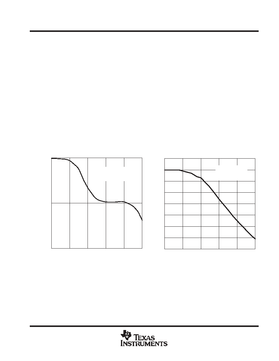
OPEN LOOP PHASE
vs.
FREQUENCY
f - Frequency - Hz
Phase - deg
10 M
1 M
100 k
10 k
1 k
100
-180
-90
0
Figure 3
CO = 100
µ
F
IL = 1 A
Figure 4
OPEN LOOP GAIN
vs.
FREQUENCY
10 M
1 M
100 k
10 k
1 k
100
-10
0
10
20
30
40
50
60
70
f - Frequency - Hz
Gain - dB
CO = 100
µ
F
IL = 1 A
UC285 1, UC285 2, UC285 3, UC285 ADJ, UC385 1, UC385 2, UC385 3, UC385 ADJ
FAST TRANSIENT RESPONSE 5 A
LOW DROPOUT REGULATOR
SLUS212E - NOVEMBER 1999 - REVISED FEBRUARY 2004
6
POST OFFICE BOX 655303
∑
DALLAS, TEXAS 75265
APPLICATION INFORMATION
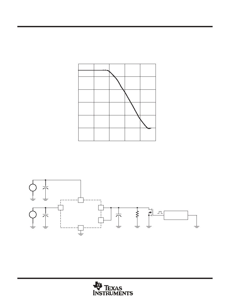
Figure 5
POWER SUPPLY REJECTION RATIO (VB INPUT)
vs.
FREQUENCY
PSSR - Power Supply Rejection Ratio (VB Input) - dB
10 M
1 M
100 k
10 k
1 k
100
0
10
20
30
40
50
60
f - Frequency - Hz
UDG-00085
4
5
1
2
3
ADJ
VOUT
VB
VIN
GND
4.7
µ
F
Tantalum
1
µ
F
Ceramic
100
µ
F
Tantalum
121
R1
UC385-ADJ
Pulse
Generator
VO = 1.2 V
IRF
520
+
+
5 V
3.3 V
_
+
_
+
Figure 6. Transient Test Circuit
UC285 1, UC285 2, UC285 3, UC285 ADJ, UC385 1, UC385 2, UC385 3, UC385 ADJ
FAST TRANSIENT RESPONSE 5 A
LOW DROPOUT REGULATOR
SLUS212E - NOVEMBER 1999 - REVISED FEBRUARY 2004
7
POST OFFICE BOX 655303
∑
DALLAS, TEXAS 75265
APPLICATION INFORMATION
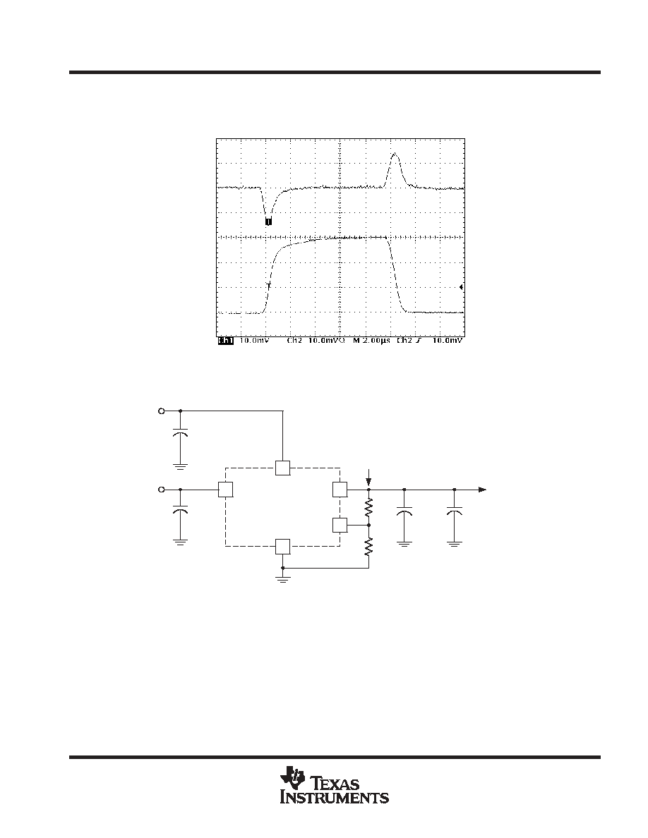
Figure 7
10 mA to 3 A/
µ
s Load Transient Response
3
2
1
0
- Load Current -
A
I O
20
10
0
-10
-20
V
O
- Change in
Output V
oltage - mV
2
µ
s/DIV
UDG-00086
4
5
1
2
3
ADJ
VOUT
VB
VIN
GND
4.7
µ
F
+3.3 V
4.7
µ
F
+5 V
330
µ
F
OSCON
UC385-ADJ
Kelvin
Sense
Point
2.2
µ
F
Ceramic
R3
60
R4
120
+1.8 V
Output
+
+
+
Figure 8. Typical UC385-ADJ Application
UC285 1, UC285 2, UC285 3, UC285 ADJ, UC385 1, UC385 2, UC385 3, UC385 ADJ
FAST TRANSIENT RESPONSE 5 A
LOW DROPOUT REGULATOR
SLUS212E - NOVEMBER 1999 - REVISED FEBRUARY 2004
8
POST OFFICE BOX 655303
∑
DALLAS, TEXAS 75265
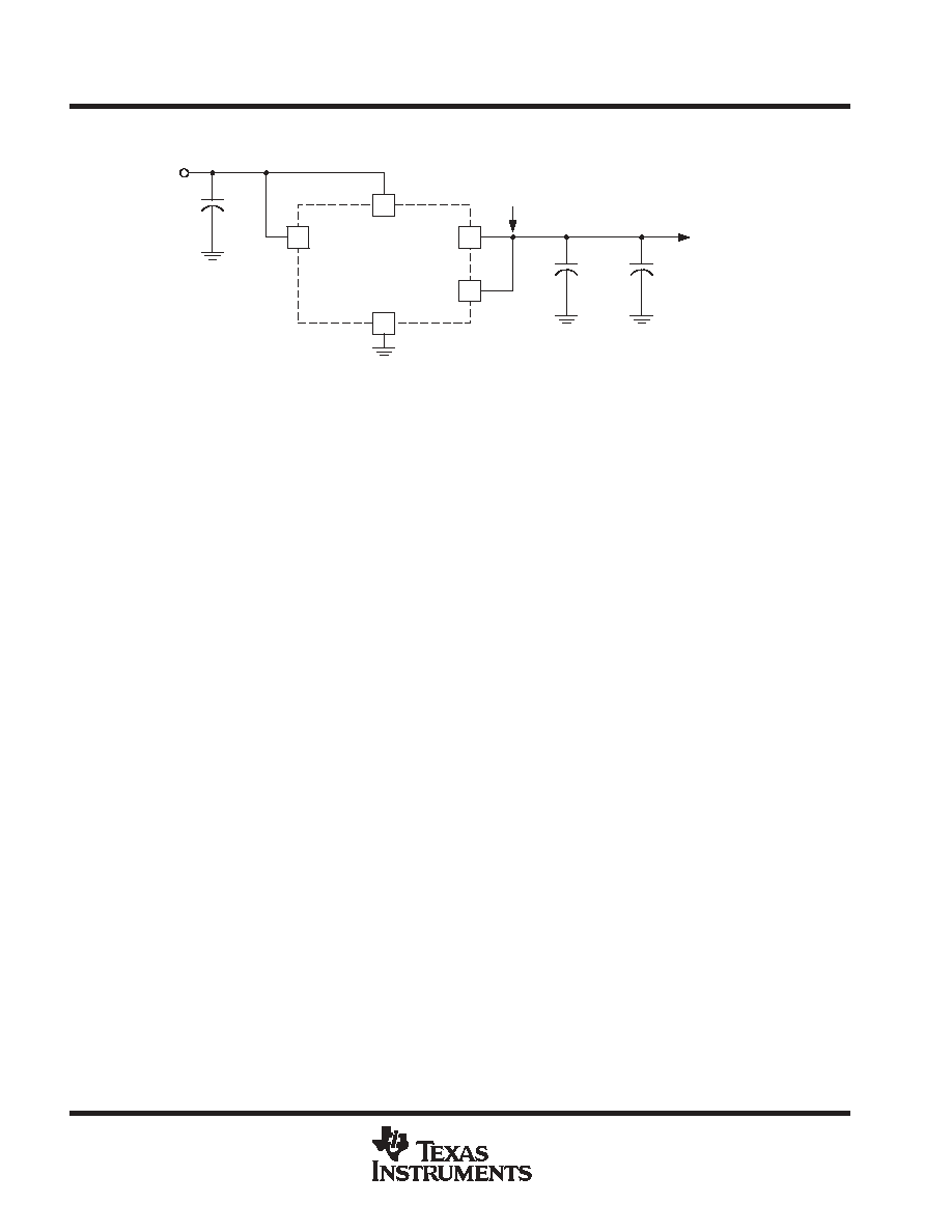
APPLICATION INFORMATION
UDG-00087
4
5
1
2
3
ADJ
VOUT
VB
VIN
GND
4.7
µ
F
+5 V
330
µ
F
OSCON
UC385-1
Kelvin
Sense
Point
2.2
µ
F
Ceramic
+1.5 V
Output
+
+
Figure 9. Typical UC385-1, -2, or -3 Application
PACKAGING INFORMATION
Orderable Device
Status
(1)
Package
Type
Package
Drawing
Pins Package
Qty
Eco Plan
(2)
Lead/Ball Finish
MSL Peak Temp
(3)
UC285T-1
ACTIVE
TO-220
KC
5
50
None
CU SN
Level-NA-NA-NA
UC285T-2
ACTIVE
TO-220
KC
5
50
None
CU SN
Level-NA-NA-NA
UC285T-3
ACTIVE
TO-220
KC
5
50
None
CU SN
Level-NA-NA-NA
UC285T-ADJ
ACTIVE
TO-220
KC
5
50
None
CU SN
Level-NA-NA-NA
UC285TD-1
OBSOLETE
DDPAK/
TO-263
KTT
5
None
Call TI
Call TI
UC285TD-2
OBSOLETE
DDPAK/
TO-263
KTT
5
None
Call TI
Call TI
UC285TD-3
OBSOLETE
DDPAK/
TO-263
KTT
5
None
Call TI
Call TI
UC285TD-ADJ
OBSOLETE
DDPAK/
TO-263
KTT
5
None
Call TI
Call TI
UC285TDKTTT-1
ACTIVE
DDPAK/
TO-263
KTT
5
50
None
CU SN
Level-2-220C-1 YEAR
UC285TDKTTT-2
ACTIVE
DDPAK/
TO-263
KTT
5
50
None
CU SN
Level-2-220C-1 YEAR
UC285TDKTTT-3
ACTIVE
DDPAK/
TO-263
KTT
5
50
None
CU SN
Level-2-220C-1 YEAR
UC285TDKTTT-ADJ
ACTIVE
DDPAK/
TO-263
KTT
5
50
None
CU SN
Level-2-220C-1 YEAR
UC285TDTR-1
ACTIVE
DDPAK/
TO-263
KTT
5
500
None
Call TI
Call TI
UC285TDTR-2
ACTIVE
DDPAK/
TO-263
KTT
5
500
None
Call TI
Call TI
UC285TDTR-3
ACTIVE
DDPAK/
TO-263
KTT
5
500
None
Call TI
Call TI
UC285TDTR-ADJ
ACTIVE
DDPAK/
TO-263
KTT
5
500
None
CU SN
Level-2-220C-1 YEAR
UC385T-1
ACTIVE
TO-220
KC
5
50
None
CU SN
Level-NA-NA-NA
UC385T-2
ACTIVE
TO-220
KC
5
50
None
CU SN
Level-NA-NA-NA
UC385T-3
ACTIVE
TO-220
KC
5
50
None
CU SN
Level-NA-NA-NA
UC385T-ADJ
ACTIVE
TO-220
KC
5
50
None
CU SN
Level-NA-NA-NA
UC385TD-1
OBSOLETE
DDPAK/
TO-263
KTT
5
None
Call TI
Call TI
UC385TD-2
OBSOLETE
DDPAK/
TO-263
KTT
5
None
Call TI
Call TI
UC385TD-3
OBSOLETE
DDPAK/
TO-263
KTT
5
None
Call TI
Call TI
UC385TD-ADJ
OBSOLETE
DDPAK/
TO-263
KTT
5
None
Call TI
Call TI
UC385TDKTTT-1
ACTIVE
DDPAK/
TO-263
KTT
5
50
None
CU SN
Level-2-220C-1 YEAR
UC385TDKTTT-2
ACTIVE
DDPAK/
TO-263
KTT
5
50
None
CU SN
Level-2-220C-1 YEAR
UC385TDKTTT-3
ACTIVE
DDPAK/
TO-263
KTT
5
50
None
CU SN
Level-2-220C-1 YEAR
UC385TDKTTT-ADJ
ACTIVE
DDPAK/
TO-263
KTT
5
50
None
CU SN
Level-2-220C-1 YEAR
PACKAGE OPTION ADDENDUM
www.ti.com
9-Dec-2004
Addendum-Page 1

Orderable Device
Status
(1)
Package
Type
Package
Drawing
Pins Package
Qty
Eco Plan
(2)
Lead/Ball Finish
MSL Peak Temp
(3)
UC385TDTR-1
ACTIVE
DDPAK/
TO-263
KTT
5
500
None
CU SN
Level-2-220C-1 YEAR
UC385TDTR-2
ACTIVE
DDPAK/
TO-263
KTT
5
500
None
CU SN
Level-2-220C-1 YEAR
UC385TDTR-3
ACTIVE
DDPAK/
TO-263
KTT
5
500
None
CU SN
Level-2-220C-1 YEAR
UC385TDTR-ADJ
ACTIVE
DDPAK/
TO-263
KTT
5
500
None
CU SN
Level-2-220C-1 YEAR
UC385TH-ADJ
OBSOLETE
TO-220
KC
5
None
Call TI
Call TI
(1)
The marketing status values are defined as follows:
ACTIVE: Product device recommended for new designs.
LIFEBUY: TI has announced that the device will be discontinued, and a lifetime-buy period is in effect.
NRND: Not recommended for new designs. Device is in production to support existing customers, but TI does not recommend using this part in
a new design.
PREVIEW: Device has been announced but is not in production. Samples may or may not be available.
OBSOLETE: TI has discontinued the production of the device.
(2)
Eco Plan - May not be currently available - please check
http://www.ti.com/productcontent
for the latest availability information and additional
product content details.
None: Not yet available Lead (Pb-Free).
Pb-Free (RoHS): TI's terms "Lead-Free" or "Pb-Free" mean semiconductor products that are compatible with the current RoHS requirements
for all 6 substances, including the requirement that lead not exceed 0.1% by weight in homogeneous materials. Where designed to be soldered
at high temperatures, TI Pb-Free products are suitable for use in specified lead-free processes.
Green (RoHS & no Sb/Br): TI defines "Green" to mean "Pb-Free" and in addition, uses package materials that do not contain halogens,
including bromine (Br) or antimony (Sb) above 0.1% of total product weight.
(3)
MSL, Peak Temp. -- The Moisture Sensitivity Level rating according to the JEDECindustry standard classifications, and peak solder
temperature.
Important Information and Disclaimer:The information provided on this page represents TI's knowledge and belief as of the date that it is
provided. TI bases its knowledge and belief on information provided by third parties, and makes no representation or warranty as to the
accuracy of such information. Efforts are underway to better integrate information from third parties. TI has taken and continues to take
reasonable steps to provide representative and accurate information but may not have conducted destructive testing or chemical analysis on
incoming materials and chemicals. TI and TI suppliers consider certain information to be proprietary, and thus CAS numbers and other limited
information may not be available for release.
In no event shall TI's liability arising out of such information exceed the total purchase price of the TI part(s) at issue in this document sold by TI
to Customer on an annual basis.
PACKAGE OPTION ADDENDUM
www.ti.com
9-Dec-2004
Addendum-Page 2
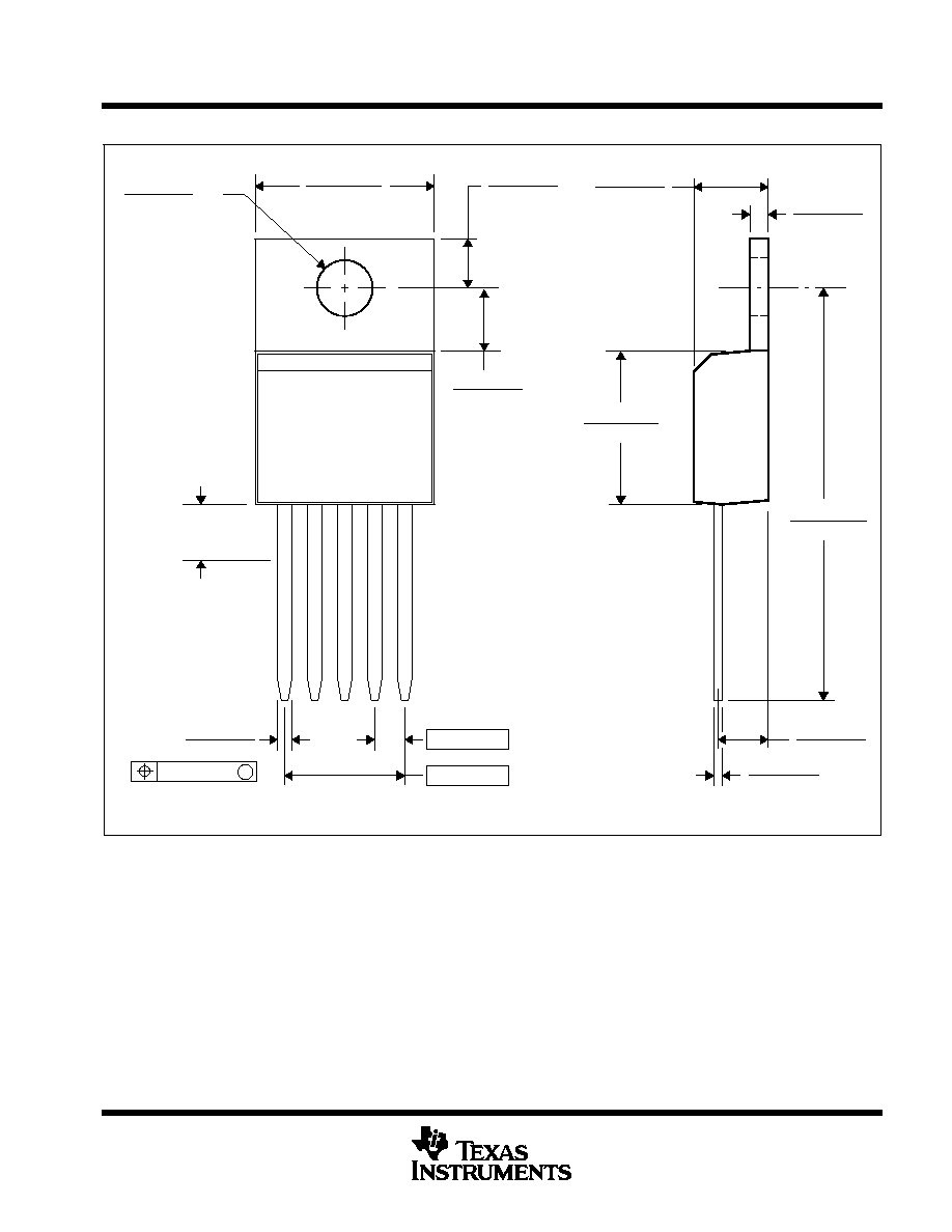
MECHANICAL DATA
MSOT008B ≠ JANUARY 1995 ≠ REVISED SEPTEMBER 2000
1
POST OFFICE BOX 655303
∑
DALLAS, TEXAS 75265
KC (R-PSFM-T5)
PLASTIC FLANGE-MOUNT
4040208/E 09/00
0.420 (10,67)
0.185 (4,70)
0.055 (1,40)
0.147 (3,73)
0.340 (8,64)
1.037 (26,34)
0.040 (1,02)
0.030 (0,76)
0.997 (25,32)
0.380 (9,65)
0.330 (8,38)
0.137 (3,48)
0.045 (1,14)
0.175 (4,46)
0.113 (2,87)
0.122 (3,10)
0.025 (0,64)
0.102 (2,59)
0.012 (0,30)
0.103 (2,62)
0.146 (3,71)
0.156 (3,96)
DIA
(see Note C)
0.125 (3,18)
0.067 (1,70)
0.268 (6,81)
5
1
M
0.010 (0,25)
NOTES: A. All linear dimensions are in inches (millimeters).
B. This drawing is subject to change without notice.
C. Lead dimensions are not controlled within this area.
D. All lead dimensions apply before solder dip.
E. The center lead is in electrical contact with the mounting tab.

IMPORTANT NOTICE
Texas Instruments Incorporated and its subsidiaries (TI) reserve the right to make corrections, modifications,
enhancements, improvements, and other changes to its products and services at any time and to discontinue
any product or service without notice. Customers should obtain the latest relevant information before placing
orders and should verify that such information is current and complete. All products are sold subject to TI's terms
and conditions of sale supplied at the time of order acknowledgment.
TI warrants performance of its hardware products to the specifications applicable at the time of sale in
accordance with TI's standard warranty. Testing and other quality control techniques are used to the extent TI
deems necessary to support this warranty. Except where mandated by government requirements, testing of all
parameters of each product is not necessarily performed.
TI assumes no liability for applications assistance or customer product design. Customers are responsible for
their products and applications using TI components. To minimize the risks associated with customer products
and applications, customers should provide adequate design and operating safeguards.
TI does not warrant or represent that any license, either express or implied, is granted under any TI patent right,
copyright, mask work right, or other TI intellectual property right relating to any combination, machine, or process
in which TI products or services are used. Information published by TI regarding third-party products or services
does not constitute a license from TI to use such products or services or a warranty or endorsement thereof.
Use of such information may require a license from a third party under the patents or other intellectual property
of the third party, or a license from TI under the patents or other intellectual property of TI.
Reproduction of information in TI data books or data sheets is permissible only if reproduction is without
alteration and is accompanied by all associated warranties, conditions, limitations, and notices. Reproduction
of this information with alteration is an unfair and deceptive business practice. TI is not responsible or liable for
such altered documentation.
Resale of TI products or services with statements different from or beyond the parameters stated by TI for that
product or service voids all express and any implied warranties for the associated TI product or service and
is an unfair and deceptive business practice. TI is not responsible or liable for any such statements.
Following are URLs where you can obtain information on other Texas Instruments products and application
solutions:
Products
Applications
Amplifiers
amplifier.ti.com
Audio
www.ti.com/audio
Data Converters
dataconverter.ti.com
Automotive
www.ti.com/automotive
DSP
dsp.ti.com
Broadband
www.ti.com/broadband
Interface
interface.ti.com
Digital Control
www.ti.com/digitalcontrol
Logic
logic.ti.com
Military
www.ti.com/military
Power Mgmt
power.ti.com
Optical Networking
www.ti.com/opticalnetwork
Microcontrollers
microcontroller.ti.com
Security
www.ti.com/security
Telephony
www.ti.com/telephony
Video & Imaging
www.ti.com/video
Wireless
www.ti.com/wireless
Mailing Address:
Texas Instruments
Post Office Box 655303 Dallas, Texas 75265
Copyright
2005, Texas Instruments Incorporated