 | –≠–ª–µ–∫—Ç—Ä–æ–Ω–Ω—ã–π –∫–æ–º–ø–æ–Ω–µ–Ω—Ç: UC2875J | –°–∫–∞—á–∞—Ç—å:  PDF PDF  ZIP ZIP |
UC1875/6/7/8
UC2875/6/7/8
UC3875/6/7/8
DESCRIPTION
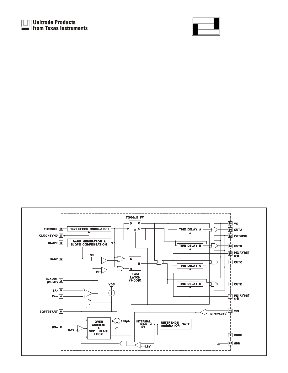
The UC1875 family of integrated circuits implements control of a bridge
power stage by phase-shifting the switching of one half-bridge with respect
to the other, allowing constant frequency pulse-width modulation in combi-
nation with resonant, zero-voltage switching for high efficiency performance
at high frequencies. This family of circuits may be configured to provide
control in either voltage or current mode operation, with a separate
over-current shutdown for fast fault protection.
A programmable time delay is provided to insert a dead-time at the turn-on
of each output stage. This delay, providing time to allow the resonant
switching action, is independently controllable for each output pair (A-B,
C-D).
With the oscillator capable of operation at frequencies in excess of 2MHz,
overall switching frequencies to 1MHz are practical. In addition to the stan-
dard free running mode, with the CLOCKSYNC pin, the user may configure
these devices to accept an external clock synchronization signal, or may
lock together up to 5 units with the operational frequency determined by
the fastest device.
Protective features include an undervoltage lockout which maintains all out-
puts in an active-low state until the supply reaches a 10.75V threshold.
1.5V hysteresis is built in for reliable, boot-strapped chip supply.
Over-current protection is provided, and will latch the outputs in the OFF
state within 70nsec of a fault. The current-fault circuitry implements
full-cycle restart operation.
(continued)
Phase Shift Resonant Controller
FEATURES
∑
Zero to 100% Duty Cycle Control
∑
Programmable Output Turn-On Delay
∑
Compatible with Voltage or Current
Mode Topologies
∑
Practical Operation at Switching
Frequencies to 1MHz
∑
Four 2A Totem Pole Outputs
∑
10MHz Error Amplifier
∑
Undervoltage Lockout
∑
Low Startup Current ≠150
µ
A
∑
Outputs Active Low During UVLO
∑
Soft-Start Control
∑
Latched Over-Current Comparator
With Full Cycle Restart
∑
Trimmed Reference
SLUS229B - JULY 1999 - REVISED JUNE 2004
BLOCK DIAGRAM
UDG-95073
application
INFO
available

2
UC1875/6/7/8
UC2875/6/7/8
UC3875/6/7/8
Dil-20 (Top View) J
or N Package
ABSOLUTE MAXIMUM RATINGS
Supply Voltage (VC, VIN) . . . . . . . . . . . . . . . . . . . . . . . . . . 20V
Output Current, Source or Sink
DC . . . . . . . . . . . . . . . . . . . . . . . . . . . . . . . . . . . . . . . . . 0.5A
Pulse (0.5
µ
s) . . . . . . . . . . . . . . . . . . . . . . . . . . . . . . . . . . 3A
Analog I/0s
(Pins 1, 2, 3, 4, 5, 6, 7, 15, 16, 17, 18, 19) . . . . ≠0.3 to 5.3V
Storage Temperature Range . . . . . . . . . . . . . ≠65∞C to +150∞C
Junction Temperature . . . . . . . . . . . . . . . . . . . ≠55∞C to +150∞C
Lead Temperature (Soldering, 10 sec.) . . . . . . . . . . . . +300∞C
Note:
Pin references are to 20 pin packages. All voltages are
with respect to ground. Currents are positive into, neg-
ative out of, device terminals. Consult Unitrode
databook for information regarding thermal specifica-
tions and limitations of packages.
SOIC-28, (Top View)
DWP Package
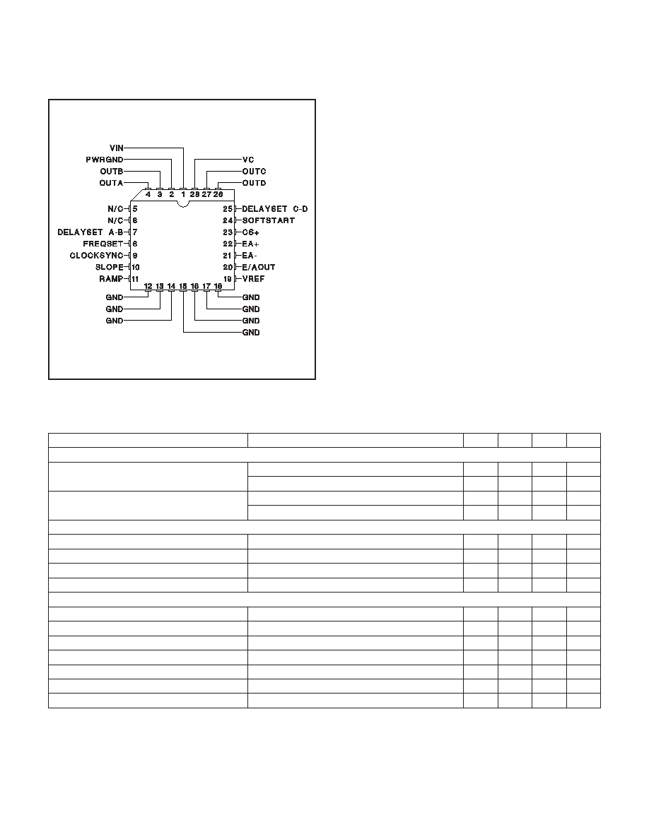
CONNECTION DIAGRAMS
4
25
24
23
OUTA
2
3
1 28
22
21
5
6
7
8
9
12
14
13
15 16
N/C
N/C
OUTC
OUTD
N/C
DELAYSET C-D
SS
CS+
EA+
DELAYSET A-B
FREQSET
CLOCKSYNC
SLOPE
RAMP
E/A-
N/C
N/C
N/C
GND
10
11
17 18
20
19
27 26
OUTB
PWRGND
VIN
N/C
E/A OUT
VREF
N/C
VC
Additional features include an error amplifier with band-
width in excess of 7MHz, a 5V reference, provisions for
soft-starting, and flexible ramp generation and slope com-
pensation circuitry.
These devices are available in 20-pin DIP, 28-pin
"bat-wing" SOIC and 28 lead power PLCC plastic pack-
ages for operation over both 0∞C to 70∞C and ≠25∞C to
+85∞C temperature ranges; and in hermetically sealed
cerdip, surface mount, and ceramic leadless chip carrier
packages for ≠55∞C to +125∞C operation.
Device
UVLO
Turn-On
UVLO
Turn-Off
Delay
Set
UC1875
10.75
9.25V
Yes
UC1876
15.25V
9.25V
Yes
UC1877
10.75V
9.25V
No
UC1878
15.25V
9.25V
No
DESCRIPTION (cont.)
CLCC-28 (Top View) L Package
3
UC1875/6/7/8
UC2875/6/7/8
UC3875/6/7/8
ELECTRICAL CHARACTERISTICS:
Unless otherwise stated, ≠55∞C < T
A
< 125∞C for the UC1875/6/7/8, ≠25∞C < T
A
<
85∞C for the UC2875/6/7/8 and 0∞C < T
A
< 70∞C for the UC3875/6/7/8, VC = VIN = 12V, R
FREQSET
= 12k
, C
FREQSET
= 330pF,
R
SLOPE
= 12k
, C
RAMP
= 200pF, C
DELAYSET A-B
= C
DELAYSET C-D
= 0.01
µ
F, I
DELAYSET A-B
= I
DELAYSET C-D
= ≠500
µ
A, T
A
= T
J
.
PARAMETER
TEST CONDITIONS
MIN
TYP
MAX
UNITS
Undervoltage Lockout
Start Threshold
UC1875/UC1877
10.75
11.75
V
UC1876/UC1878
15.25
V
UVLO Hysteresis
UC1875/UC1877
0.5
1.25
2.0
V
UC1876/UC1878
6.0
V
Supply Current
I
IN
Startup
VIN = 8V, VC = 20V, R
SLOPE
open, I
DELAY
= 0
150
600
µ
A
I
C
Startup
VIN = 8V, VC = 20V, R
SLOPE
open, I
DELAY
= 0
10
100
µ
A
I
IN
30
44
mA
I
C
15
30
mA
Voltage Reference
Output Voltage
T
J
= +25∞C
4.92
5
5.08
V
Line Regulation
11 < VIN < 20V
1
10
mV
Load Regulation
I
VREF
= ≠10mA
5
20
mV
Total Variation
Line, Load, Temperature
4.9
5.1
V
Noise Voltage
10Hz to 10kHz
50
µ
Vrms
Long Term Stability
T
J
= 125∞C, 1000 hours
2.5
mV
Short Circuit Current
VREF = 0V, T
J
= 25∞C
60
mA
PLCC-28 (Top View)
QP Package

4
UC1875/6/7/8
UC2875/6/7/8
UC3875/6/7/8
ELECTRICAL CHARACTERISTICS:
Unless otherwise stated, ≠55∞C < T
A
< 125∞C for the UC1875/6/7/8, ≠25∞C < T
A
<
85∞C for the UC2875/6/7/8 and 0∞C < T
A
< 70∞C for the UC3875/6/7/8, VC = VIN = 12V, R
FREQSET
= 12k
, C
FREQSET
= 330pF,
R
SLOPE
= 12k
, C
RAMP
= 200pF, C
DELAYSET A-B
= C
DELAYSET C-D
= 0.01
µ
F, I
DELAYSET A-B
= I
DELAYSET C-D
= ≠500
µ
A, T
A
= T
J
.
PARAMETER
TEST CONDITIONS
MIN
TYP
MAX
UNITS
Error Amplifier
Offset Voltage
5
15
mV
Input Bias Current
0.6
3
µ
A
AVOL
1V < V
E/AOUT
< 4V
60
90
dB
CMRR
1.5V < V
CM
< 5.5V
75
95
dB
PSRR
11V < VIN < 20V
85
100
dB
Output Sink Current
V
E/AOUT
= 1V
1
2.5
mA
Output Source Current
V
E/AOUT
= 4V
≠1.3
≠0.5
mA
Output Voltage High
I
E/AOUT
= ≠0.5mA
4
4.7
5
V
Output Voltage Low
I
E/AOUT
= 1mA
0
0.5
1
V
Unity Gain BW
(Note 8)
7
11
MHz
Slew Rate
(Note 8)
6
11
V/
µ
sec
PWM Comparator
Ramp Offset Voltage
T
J
= 25∞C (Note 3)
1.3
V
Zero Phase Shift Voltage
(Note 4)
0.55
0.9
V
PWM Phase Shift (Note1) and (Note 7)
V
E/AOUT
> (Ramp Peak + Ramp Offset)
98
99.5
102
%
V
E/AOUT
< Zero Phase Shift Voltage
0
0.5
2
%
Output Skew (Note 1) and (Note 7)
V
E/AOUT
< 1V
5
±20
nsec
Ramp to Output Delay, (Note 8)
UC3875/6/7/8 (Note 6)
65
100
nsec
UC1875/6/7/8, UC2875/6/7/8 (Note 6)
65
125
nsec
Oscillator
Initial Accuracy
T
J
= 25∞C
0.85
1
1.15
MHz
Voltage Stability
11V < VIN < 20V
0.2
2
%
Total Variation
Line, Temperature
0.80
1.20
MHz
Sync Pin Threshold
T
J
= 25∞C
3.8
V
Clock Out Peak
T
J
= 25∞C
4.3
V
Clock Out Low
T
J
= 25∞C
3.3
V
Clock Out Pulse Width
R
CLOCKSYNC
= 3.9k
30
100
nsec
Maximum Frequency, (Note 7)
R
FREQSET
= 5k
2
MHz
Ramp Generator/Slope Compensation
Ramp Current, Minimum
I
SLOPE
= 10
µ
A, V
FREQSET
= VREF
≠11
≠14
µ
A
Ramp Current, Maximum
I
SLOPE
= 1mA, V
FREQSET
= VREF
≠0.8
≠0.95
mA
Ramp Valley
0
V
Ramp Peak - Clamping Level
R
FREQSET
= 100k
3.8
4.1
V
Current Limit
Input Bias
V
CS
+ = 3V
2
5
µ
A
Threshold Voltage
2.4
2.5
2.6
V
Delay to Output, (Note 8)
UC3875/6/7/8
85
125
nsec
UC1875/6/7/8, UC2875/6/7/8
85
150
nsec
5
UC1875/6/7/8
UC2875/6/7/8
UC3875/6/7/8
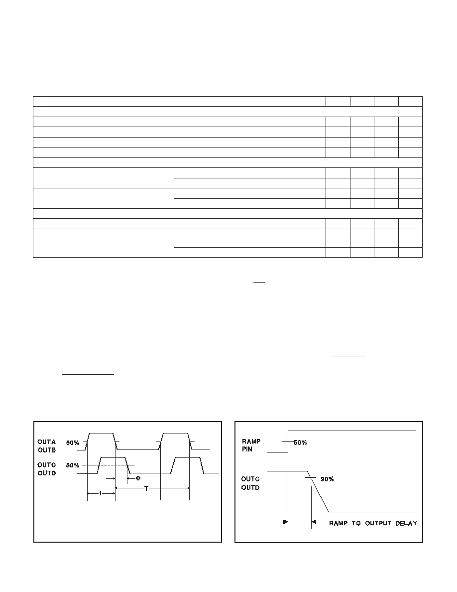
Note 1: Phase shift percentage (0% = 0∞, 100% = 180∞) is defined as
=
200
T
%, where q is the phase shift, and F and T are de-
fined in Figure 1. At 0% phase shift,
F is the output skew.
Note 2: Delay time is defined as delay = T (1/2≠(duty cycle)), where T is defined in Fig. 1.
Note 3: Ramp offset voltage has a temperature coefficient of about ≠4mV/∞C.
Note 4: Zero phase shift voltage has a temperature coefficient of about ≠2mV/∞C.
Note 5: Delay time can be programmed via resistors from the delay set pins to ground. Delay time
∑
62 5 10
12
.
≠
I
DELAY
sec. Where
I
DELAY
=
De lay s e t voltage
R
DELAY
The recommended range for I
DELAY
is 25
mA £ I
DELAY
£ 1mA
Note 6: Ramp delay to output time is defined in Fig. 2.
Note 7: Not production tested at -55
∞
C.
Duty Cycle = t/T
Period = T
T
DHL
(A to C) = T
DHL
(B to D) =
Phase Shift, Output Skew & Delay Time Definitions
UDG-95074
Figure 1
Figure 2
UDG-95075
ELECTRICAL CHARACTERISTICS:
Unless otherwise stated, ≠55∞C < T
A
< 125∞C for the UC1875/6/7/8, ≠25∞C < T
A
<
85∞C for the UC2875/6/7/8 and 0∞C < T
A
< 70∞C for the UC3875/6/7/8, VC = VIN = 12V, R
FREQSET
= 12k
, C
FREQSET
= 330pF,
R
SLOPE
= 12k
, C
RAMP
= 200pF, C
DELAYSET A-B
= C
DELAYSET C-D
= 0.01
µ
F, I
DELAYSET A-B
= I
DELAYSET C-D
= ≠500
µ
A, T
A
= T
J
.
PARAMETER
TEST CONDITIONS
MIN
TYP
MAX
UNITS
Soft-Start/Reset Delay
Charge Current
V
SOFTSTART
= 0.5V
≠20
≠9
≠3
µ
A
Discharge Current
V
SOFTSTART
= 1V
120
230
µ
A
Restart Threshold
4.3
4.7
V
Discharge Level
300
mV
Output Drivers
Output Low Level
I
OUT
= 50mA
0.2
0.4
V
I
OUT
= 500mA
1.2
2.6
V
Output High Level
I
OUT
= ≠50mA
1.5
2.5
V
I
OUT
= ≠500mA
1.7
2.6
V
Delay Set (UC1875 and UC1876 only)
Delay Set Voltage
I
DELAY
= ≠500
µ
A
2.3
2.4
2.6
V
Delay Time, (Note 8)
I
DELAY
= ≠250
µ
A (Note 5) (UC3875/6/7/8,
UC2875/6/7/8)
150
250
400
nsec
I
DELAY
= ≠250
µ
A (Note 5) (UC1875/6/7/8)
150
250
600
nsec

6
UC1875/6/7/8
UC2875/6/7/8
UC3875/6/7/8
CLOCKSYNC (bi-directional clock and synchronization
pin): Used as an output, this pin provides a clock signal.
As an input, this pin provides a synchronization point. In
its simplest usage, multiple devices, each with their own
local oscillator frequency, may be connected together by
the CLOCKSYNC pin and will synchronize on the fastest
oscillator. This pin may also be used to synchronize the
device to an external clock, provided the external signal
is of higher frequency than the local oscillator. A resistor
load may be needed on this pin to minimize the clock
pulse width.
E/AOUT (error amplifier output):
This is is the gain stage
for overall feedback control. Error amplifier output volt-
age levels below 1 volt will force 0∞ phase shift. Since the
error amplifier has a relatively low current drive capabil-
ity, the output may be overridden by driving with a suffi-
ciently low impedance source.
CS+ (current sense):The non-inverting input to the cur-
rent-fault comparator whose reference is set internally to
a fixed 2.5V (separate from VREF). When the voltage at
this pin exceeds 2.5V the current-fault latch is set, the
outputs are forced OFF and a SOFT-START cycle is initi-
ated. If a constant voltage above 2.5V is applied to this
pin the outputs are disabled from switching and held in a
low state until the CS+ pin is brought below 2.5V. The
outputs may begin switching at 0 degrees phase shift be-
fore the SOFTSTART pin begins to rise -- this condition
will not prematurely deliver power to the load.
FREQSET (oscillator frequency set pin):
A resistor and a
capacitor from FREQSET to GND will set the oscillator
frequency.
DELAYSET A-B, DELAYSET C-D (output delay control):
The user programmed current flowing from these pins to
GND set the turn-on delay for the corresponding output
pair. This delay is introduced between turn-off of one
switch and turn-on of another in the same leg of the
bridge to provide a dead time in which the resonant
switching of the external power switches takes place.
Separate delays are provided for the two half-bridges to
accommodate differences in the resonant capacitor
charging currents.
EA≠ (error amplifier inverting input):
This is normally con-
nected to the voltage divider resistors which sense the
power supply output voltage level.
EA+ (error amplifier non-inverting input):
This is normally
connected to a reference voltage used for comparison
with the sensed power supply output voltage level at the
EA+ pin.
GND (signal ground):All voltages are measured with re-
spect to GND. The timing capacitor, on the FREQSET
pin, any bypass capacitor on the VREF pin, bypass ca-
pacitors on VIN and the ramp capacitor, on the RAMP
pin, should be connected directly to the ground plane
near the signal ground pin.
OUTA-OUTD (outputs A-D): The outputs are 2A to-
tem-pole drivers optimized for both MOSFET gates and
level-shifting transformers. The outputs operate as pairs
with a nominal 50% duty-cycle. The A-B pair is intended
to drive one half-bridge in the external power stage and
is syncronized with the clock waveform. The C-D pair
will drive the other half-bridge with switching phase
shifted with respect to the A-B outputs.
PWRGND (power ground):VC should be bypassed with
a ceramic capacitor from the VC pin to the section of the
ground plane that is connected to PWRGND. Any re-
quired bulk reservoir capacitor should parallel this one.
Power ground and signal ground may be joined at a sin-
gle point to optimize noise rejection and minimize DC
drops.
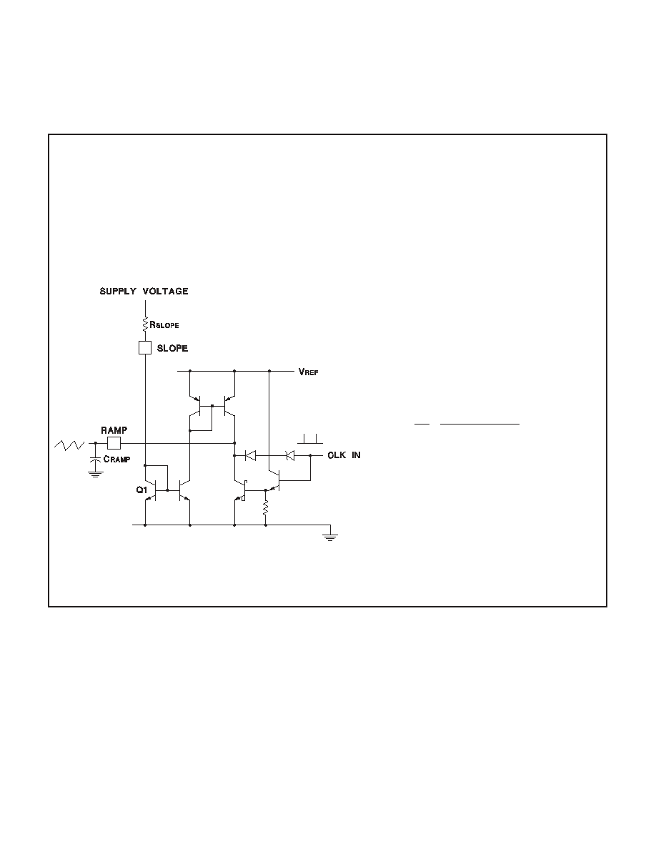
RAMP (voltage ramp):This pin is the input to the PWM
comparator. Connect a capacitor from here to GND. A
voltage ramp is developed at this pin with a slope:
dV
dT
S e ns e Voltage
R
C
S LOPE
R AMP
=
∑
Current mode control may be achieved with a minimum
amount of external circuitry, in which case this pin pro-
vides slope compensation.
Because of the 1.3V offset between the ramp input and
the PWM comparator, the error amplifier output voltage
can not exceed the effective ramp peak voltage and duty
cycle clamping is easily achievable with appropriate val-
ues of R
SLOPE
and C
RAMP
.
SLOPE (set ramp slope/slope compensation):
A resistor
from this pin to VCC will set the current used to generate
the ramp. Connecting this resistor to the DC input line
voltage will provide voltage feed-forward.
SOFTSTART (soft start): SOFTSTART will remain at
GND as long as VIN is below the UVLO threshold.
SOFTSTART will be pulled up to about 4.8V by an inter-
nal 9
µ
A current source when VIN becomes valid (assum-
ing a non-fault condition). In the event of a current-fault
(CS+ voltage exceeding 2.5V), SOFTSTART will be
pulled to GND and them ramp to 4.8V. If a fault occurs
during the SOFTSTART cycle, the outputs will be imme-
diately disabled and SOFTSTART must charge fully prior
to resetting the fault latch.
For paralleled controllers, the SOFTSTART pins may be
paralled to a single capacitor, but the charge currents will
be additive.
PIN DESCRIPTIONS
7
UC1875/6/7/8
UC2875/6/7/8
UC3875/6/7/8
VC (output switch supply voltage):This pin supplies
power to the output drivers and their associated bias cir-
cuitry. Connect VC to a stable source above 3V for nor-
mal operation, above 12V for best performance. This
supply should be bypassed directly to the PWRGND pin
with low ESR, low ESL capacitors.
VIN (primary chip supply voltage):
This pin supplies
power to the logic and analog circuitry on the integrated
circuit that is not directly associated with driving the out-
put stages. Connect VIN to a stable source above 12V
for normal operation. To ensure proper chip functionality,
these devices will be inactive until VIN exceeds the up-
per undervoltage lockout threshold. This pin should by
bypassed directly to the GND pin with low ESR, low ESL
capacitors.
NOTE: When VIN exceeds the UVLO threshold the sup-
ply current (I
IN
) will jump from about 100
µ
A to a current
in excess of 20
µ
A. If the UC1875 is not connected to a
well bypassed supply, it may immediately enter UVLO
again.
VREF: This pin is an accurate 5V voltage reference. This
output is capable of delivering about 60mA to peripheral
circuitry and is internally short circuit current limited.
VREF is disabled while VIN is low enough to force the
chip into UVLO. The circuit is also in UVLO until VREF
reaches approximately 4.75V. For best results bypass
VREF with a 0.1
µ
F, low ESR, low ESL, capacitor to the
GND pin.
PIN DESCRIPTIONS (cont.)
When power is applied to the circuit and VIN is below
the upper UVLO threshold, I
IN
will be below 600
µ
A, the
reference generator will be off, the fault latch is reset,
the soft-start pin is discharged, and the outputs are ac-
tively held low. When VIN exceeds the upper UVLO
threshold, the reference generator turns on. All else re-
mains in the shut-down mode until the output of the ref-
erence, VREF, exceeds 4.75V.
APPLICATION INFORMATION
Undervoltage Lockout Section
UDG-99136
GATE
REFERENCE
GENERATOR
VIN
10.75V/9.25V
VREF
GND
INTERNAL
BIAS
4.75V
TO SOFT-
START
LOGIC
Simplified Oscillator Schematic
UDG-95077
UDG-95079
UDG-95078
The
high
frequency
oscillator
may
be
either
free-running
or
externally
synchronized.
For
free-running operation, the frequency is set via an ex-
ternal resistor and capacitor to ground from the
FREQSET pin.

8
UC1875/6/7/8
UC2875/6/7/8
UC3875/6/7/8
APPLICATION INFORMATION (cont.)
Synchronizing The Oscillator
The CLOCKSYNC pin of the oscillator may be used to synchronize multiple UC1875 devices simply by connecting
the CLOCKSYNC of each UC1875 to the others:
Syncing to external TTL/CMOS
All ICs will sync to chip with the fastest local oscillator.
R1 & RN
may
be needed to keep sync pulse narrow due to capacitance on line.
R1 & RN
may
also be needed to properly terminate R
SYNC
line.
Although each UC1875/6/7/8 has a local oscillator fre-
quency, the group of devices will synchronize to the
fastest oscillator driving the CLOCKSYNC pin. This ar-
rangement allows the synchronizing connection be-
tween ICs to be broken without any local loss of
functionality.
Synchronizing the device to an external clock signal
may be accomplished with a minimum of external cir-
cuitry, as shown in the previous figure.
Capacitive loading on the CLOCKSYNC pin will in-
crease the clock pulse width, and may adversely effect
system performance. Therefore, a resistor to ground
from the CLOCKSYNC pin is optional, but may be re-
quired to offset capacitive loading on this pin. These re-
sistors are shown in the oscillator schematics as R1,
RN.
ICs will sync to fastest chip or TTL clock if it is higher frequency.
R & RN
may
be needed for same reasons as above
UDG-95080
UDG-95081
1875/6/7/8s only
9
UC1875/6/7/8
UC2875/6/7/8
UC3875/6/7/8
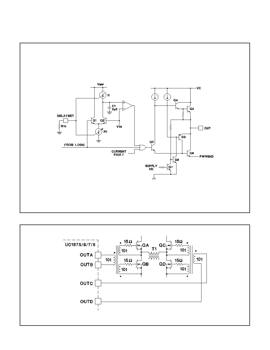
In each of the output stages, transistors Q3 through Q6
form a high-speed totem-pole driver which will source
or sink more than one amp peak with a total delay of
approximately 30 nanoseconds. To ensure a low output
level prior to turn-on, transistors Q7 through Q9 form a
self-biased driver to hold Q6 on prior to the supply
reaching its turn-on threshold. This circuit is operable
when the chip supply is zero. Q6 is also turned on and
held low with a signal from the fault logic portion of the
chip.
APPLICATION INFORMATION (cont.)
Delay Blocks And Output Stages
The delay providing the dead-time is accomplished with
C1 which must discharge to V
TH
before the output can
go high. The time is defined by the current sources, I1,
which is programmed by an external resistor, R
TD
. The
voltage on the Delay Set pins is internally regulated to
2.5V and the range of dead time control is
from 50 to 200 nanoseconds. NOTE: There is no way
to disable the delay circuitry, and the delay time must
be programmed.
The four outputs of the UC1875/6/7/8 interface to the full bridge converter switches as shown below:
Output Switch Orientation
UDG-95083
UDG-95082
3 Winding Bifilar, AWG 30 Kynar Insulation
10
UC1875/6/7/8
UC2875/6/7/8
UC3875/6/7/8
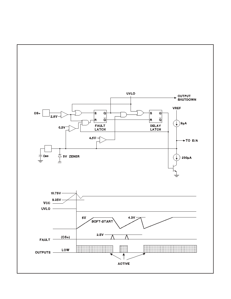
The fault control circuitry provides two forms of power
shutdown:
∑ Complete turn-off of all four output power stages.
∑ Clamping the phase shift command to zero.
Complete turn-off is ordered for an over-current fault or
a low supply voltage. When the SOFTSTART pin
reaches its low threshold, switching is allowed to pro-
ceed while the phase-shift is advanced from zero to its
nominal
value
with
the
time
constant
of
the
SOFT-START capacitor.
The fault logic insures that a continuous fault will insti-
tute a low frequency "hiccup" retry cycle by forcing the
SOFT-START capacitor to charge through its full cycle
between each restart attempt.
APPLICATION INFORMATION (cont.)
Fault/Soft-Start
UDG-95085
UDG-95084
11
UC1875/6/7/8
UC2875/6/7/8
UC3875/6/7/8
APPLICATIONS INFORMATION (cont.)
Slope/Ramp Pins
The ramp generator may be configured for the following
control methods:
∑ Voltage Mode
∑ Voltage Feedforward
∑ Current Mode
∑ Current Mode with Slope Compensation
The figure below shows a voltage-mode configuration.
With R
SLOPE
tied to a stable voltage source, the wave-
form on C
RAMP
will be a constant-slope ramp, providing
conventional voltage-mode control. If R
SLOPE
is con-
nected to the power supply input voltage, a vari-
able-slope ramp will provide voltage feedforward.
For current-mode control the ramp generator may be disabled by grounding the slope pin and using the ramp pin
as a direct current sense input to the PWM comparator.
Voltage Mode Operation
1.
Simple
voltage
mode
operation
achieved by placing R
SLOPE
between VIN
and SLOPE.
2. Voltage Feedforward achieved by plac-
ing R
SLOPE
between supply voltage and
SLOPE pin of UC1875.
RAMP
dV
dT
V
R
C
R s lope
S LOPE
R AMP
∑
UDG-95086
If you should have questions or need additional information, please contact Jody Bustamante at (903) 868-6132 or
j-busta@ti.com.
CONTACT INFORMATION

PACKAGING INFORMATION
Orderable Device
Status
(1)
Package
Type
Package
Drawing
Pins Package
Qty
Eco Plan
(2)
Lead/Ball Finish
MSL Peak Temp
(3)
5962-9455501M3A
ACTIVE
LCCC
FK
28
1
TBD
POST-PLATE
Level-NC-NC-NC
5962-9455501MRA
ACTIVE
CDIP
J
20
1
TBD
A42 SNPB
Level-NC-NC-NC
5962-9455501MXA
OBSOLETE
TO-92
LP
28
TBD
Call TI
Call TI
5962-9455501V3A
ACTIVE
LCCC
FK
28
1
TBD
Call TI
Level-NC-NC-NC
5962-9455501VRA
ACTIVE
CDIP
J
20
1
TBD
Call TI
Level-NC-NC-NC
UC1875J
ACTIVE
CDIP
J
20
1
TBD
A42 SNPB
Level-NC-NC-NC
UC1875J883B
ACTIVE
CDIP
J
20
1
TBD
A42 SNPB
Level-NC-NC-NC
UC1875JQMLV
ACTIVE
CDIP
J
20
TBD
Call TI
Call TI
UC1875L
ACTIVE
LCCC
FK
28
1
TBD
POST-PLATE
Level-NC-NC-NC
UC1875L883B
ACTIVE
LCCC
FK
28
1
TBD
POST-PLATE
Level-NC-NC-NC
UC2875DWP
ACTIVE
SOIC
DW
28
20
Green (RoHS &
no Sb/Br)
CU NIPDAU
Level-2-260C-1 YEAR
UC2875DWPG4
ACTIVE
SOIC
DW
28
20
Green (RoHS &
no Sb/Br)
CU NIPDAU
Level-2-260C-1 YEAR
UC2875DWPTR
ACTIVE
SOIC
DW
28
1000 Green (RoHS &
no Sb/Br)
CU NIPDAU
Level-2-260C-1 YEAR
UC2875DWPTRG4
ACTIVE
SOIC
DW
28
1000 Green (RoHS &
no Sb/Br)
CU NIPDAU
Level-2-260C-1 YEAR
UC2875J
ACTIVE
CDIP
J
20
1
TBD
A42 SNPB
Level-NC-NC-NC
UC2875N
ACTIVE
PDIP
N
20
20
Green (RoHS &
no Sb/Br)
CU NIPDAU
Level-NC-NC-NC
UC2875NG4
ACTIVE
PDIP
N
20
20
Green (RoHS &
no Sb/Br)
CU NIPDAU
Level-NA-NA-NA
UC2875QP
ACTIVE
PLCC
FN
28
37
TBD
Call TI
Level-2-220C-1 YEAR
UC2876N
ACTIVE
PDIP
N
20
20
Green (RoHS &
no Sb/Br)
CU NIPDAU
Level-NC-NC-NC
UC3875DWP
ACTIVE
SOIC
DW
28
20
Green (RoHS &
no Sb/Br)
CU NIPDAU
Level-2-260C-1 YEAR
UC3875DWPG4
ACTIVE
SOIC
DW
28
20
Green (RoHS &
no Sb/Br)
CU NIPDAU
Level-2-260C-1 YEAR
UC3875DWPTR
ACTIVE
SOIC
DW
28
1000 Green (RoHS &
no Sb/Br)
CU NIPDAU
Level-2-260C-1 YEAR
UC3875DWPTRG4
ACTIVE
SOIC
DW
28
1000 Green (RoHS &
no Sb/Br)
CU NIPDAU
Level-2-260C-1 YEAR
UC3875N
ACTIVE
PDIP
N
20
20
Green (RoHS &
no Sb/Br)
CU NIPDAU
Level-NC-NC-NC
UC3875NG4
ACTIVE
PDIP
N
20
20
Green (RoHS &
no Sb/Br)
CU NIPDAU
Level-NC-NC-NC
UC3875QP
ACTIVE
PLCC
FN
28
37
TBD
Call TI
Level-2-220C-1 YEAR
UC3875QPTR
ACTIVE
PLCC
FN
28
750
TBD
Call TI
Level-2-220C-1 YEAR
UC3876N
ACTIVE
PDIP
N
20
20
Green (RoHS &
no Sb/Br)
CU NIPDAU
Level-NC-NC-NC
UC3877DWPTR
ACTIVE
SOIC
DW
28
1000 Green (RoHS &
no Sb/Br)
CU NIPDAU
Level-2-260C-1 YEAR
(1)
The marketing status values are defined as follows:
ACTIVE: Product device recommended for new designs.
LIFEBUY: TI has announced that the device will be discontinued, and a lifetime-buy period is in effect.
PACKAGE OPTION ADDENDUM
www.ti.com
19-Oct-2005
Addendum-Page 1

NRND: Not recommended for new designs. Device is in production to support existing customers, but TI does not recommend using this part in
a new design.
PREVIEW: Device has been announced but is not in production. Samples may or may not be available.
OBSOLETE: TI has discontinued the production of the device.
(2)
Eco
Plan
-
The
planned
eco-friendly
classification:
Pb-Free
(RoHS)
or
Green
(RoHS
&
no
Sb/Br)
-
please
check
http://www.ti.com/productcontent
for the latest availability information and additional product content details.
TBD: The Pb-Free/Green conversion plan has not been defined.
Pb-Free (RoHS): TI's terms "Lead-Free" or "Pb-Free" mean semiconductor products that are compatible with the current RoHS requirements
for all 6 substances, including the requirement that lead not exceed 0.1% by weight in homogeneous materials. Where designed to be soldered
at high temperatures, TI Pb-Free products are suitable for use in specified lead-free processes.
Green (RoHS & no Sb/Br): TI defines "Green" to mean Pb-Free (RoHS compatible), and free of Bromine (Br) and Antimony (Sb) based flame
retardants (Br or Sb do not exceed 0.1% by weight in homogeneous material)
(3)
MSL, Peak Temp. -- The Moisture Sensitivity Level rating according to the JEDEC industry standard classifications, and peak solder
temperature.
Important Information and Disclaimer:The information provided on this page represents TI's knowledge and belief as of the date that it is
provided. TI bases its knowledge and belief on information provided by third parties, and makes no representation or warranty as to the
accuracy of such information. Efforts are underway to better integrate information from third parties. TI has taken and continues to take
reasonable steps to provide representative and accurate information but may not have conducted destructive testing or chemical analysis on
incoming materials and chemicals. TI and TI suppliers consider certain information to be proprietary, and thus CAS numbers and other limited
information may not be available for release.
In no event shall TI's liability arising out of such information exceed the total purchase price of the TI part(s) at issue in this document sold by TI
to Customer on an annual basis.
PACKAGE OPTION ADDENDUM
www.ti.com
19-Oct-2005
Addendum-Page 2
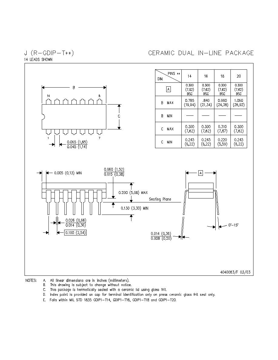
MECHANICAL DATA
MLCC006B ≠ OCTOBER 1996
POST OFFICE BOX 655303
∑
DALLAS, TEXAS 75265
FK (S-CQCC-N**)
LEADLESS CERAMIC CHIP CARRIER
4040140 / D 10/96
28 TERMINAL SHOWN
B
0.358
(9,09)
MAX
(11,63)
0.560
(14,22)
0.560
0.458
0.858
(21,8)
1.063
(27,0)
(14,22)
A
NO. OF
MIN
MAX
0.358
0.660
0.761
0.458
0.342
(8,69)
MIN
(11,23)
(16,26)
0.640
0.739
0.442
(9,09)
(11,63)
(16,76)
0.962
1.165
(23,83)
0.938
(28,99)
1.141
(24,43)
(29,59)
(19,32)
(18,78)
**
20
28
52
44
68
84
0.020 (0,51)
TERMINALS
0.080 (2,03)
0.064 (1,63)
(7,80)
0.307
(10,31)
0.406
(12,58)
0.495
(12,58)
0.495
(21,6)
0.850
(26,6)
1.047
0.045 (1,14)
0.045 (1,14)
0.035 (0,89)
0.035 (0,89)
0.010 (0,25)
12
13
14
15
16
18
17
11
10
8
9
7
5
4
3
2
0.020 (0,51)
0.010 (0,25)
6
1
28
26
27
19
21
B SQ
A SQ
22
23
24
25
20
0.055 (1,40)
0.045 (1,14)
0.028 (0,71)
0.022 (0,54)
0.050 (1,27)
NOTES: A. All linear dimensions are in inches (millimeters).
B. This drawing is subject to change without notice.
C. This package can be hermetically sealed with a metal lid.
D. The terminals are gold plated.
E. Falls within JEDEC MS-004

MECHANICAL DATA
MPLC004A ≠ OCTOBER 1994
1
POST OFFICE BOX 655303
∑
DALLAS, TEXAS 75265
FN (S-PQCC-J**)
PLASTIC J-LEADED CHIP CARRIER
4040005 / B 03/95
20 PIN SHOWN
0.026 (0,66)
0.032 (0,81)
D2 / E2
0.020 (0,51) MIN
0.180 (4,57) MAX
0.120 (3,05)
0.090 (2,29)
D2 / E2
0.013 (0,33)
0.021 (0,53)
Seating Plane
MAX
D2 / E2
0.219 (5,56)
0.169 (4,29)
0.319 (8,10)
0.469 (11,91)
0.569 (14,45)
0.369 (9,37)
MAX
0.356 (9,04)
0.456 (11,58)
0.656 (16,66)
0.008 (0,20) NOM
1.158 (29,41)
0.958 (24,33)
0.756 (19,20)
0.191 (4,85)
0.141 (3,58)
MIN
0.441 (11,20)
0.541 (13,74)
0.291 (7,39)
0.341 (8,66)
18
19
14
13
D
D1
1
3
9
E1
E
4
8
MIN
MAX
MIN
PINS
**
20
28
44
0.385 (9,78)
0.485 (12,32)
0.685 (17,40)
52
68
84
1.185 (30,10)
0.985 (25,02)
0.785 (19,94)
D / E
0.395 (10,03)
0.495 (12,57)
1.195 (30,35)
0.995 (25,27)
0.695 (17,65)
0.795 (20,19)
NO. OF
D1 / E1
0.350 (8,89)
0.450 (11,43)
1.150 (29,21)
0.950 (24,13)
0.650 (16,51)
0.750 (19,05)
0.004 (0,10)
M
0.007 (0,18)
0.050 (1,27)
NOTES: A. All linear dimensions are in inches (millimeters).
B. This drawing is subject to change without notice.
C. Falls within JEDEC MS-018

IMPORTANT NOTICE
Texas Instruments Incorporated and its subsidiaries (TI) reserve the right to make corrections, modifications,
enhancements, improvements, and other changes to its products and services at any time and to discontinue
any product or service without notice. Customers should obtain the latest relevant information before placing
orders and should verify that such information is current and complete. All products are sold subject to TI's terms
and conditions of sale supplied at the time of order acknowledgment.
TI warrants performance of its hardware products to the specifications applicable at the time of sale in
accordance with TI's standard warranty. Testing and other quality control techniques are used to the extent TI
deems necessary to support this warranty. Except where mandated by government requirements, testing of all
parameters of each product is not necessarily performed.
TI assumes no liability for applications assistance or customer product design. Customers are responsible for
their products and applications using TI components. To minimize the risks associated with customer products
and applications, customers should provide adequate design and operating safeguards.
TI does not warrant or represent that any license, either express or implied, is granted under any TI patent right,
copyright, mask work right, or other TI intellectual property right relating to any combination, machine, or process
in which TI products or services are used. Information published by TI regarding third-party products or services
does not constitute a license from TI to use such products or services or a warranty or endorsement thereof.
Use of such information may require a license from a third party under the patents or other intellectual property
of the third party, or a license from TI under the patents or other intellectual property of TI.
Reproduction of information in TI data books or data sheets is permissible only if reproduction is without
alteration and is accompanied by all associated warranties, conditions, limitations, and notices. Reproduction
of this information with alteration is an unfair and deceptive business practice. TI is not responsible or liable for
such altered documentation.
Resale of TI products or services with statements different from or beyond the parameters stated by TI for that
product or service voids all express and any implied warranties for the associated TI product or service and
is an unfair and deceptive business practice. TI is not responsible or liable for any such statements.
Following are URLs where you can obtain information on other Texas Instruments products and application
solutions:
Products
Applications
Amplifiers
amplifier.ti.com
Audio
www.ti.com/audio
Data Converters
dataconverter.ti.com
Automotive
www.ti.com/automotive
DSP
dsp.ti.com
Broadband
www.ti.com/broadband
Interface
interface.ti.com
Digital Control
www.ti.com/digitalcontrol
Logic
logic.ti.com
Military
www.ti.com/military
Power Mgmt
power.ti.com
Optical Networking
www.ti.com/opticalnetwork
Microcontrollers
microcontroller.ti.com
Security
www.ti.com/security
Telephony
www.ti.com/telephony
Video & Imaging
www.ti.com/video
Wireless
www.ti.com/wireless
Mailing Address:
Texas Instruments
Post Office Box 655303 Dallas, Texas 75265
Copyright
2005, Texas Instruments Incorporated