 | –≠–ª–µ–∫—Ç—Ä–æ–Ω–Ω—ã–π –∫–æ–º–ø–æ–Ω–µ–Ω—Ç: UC2903J | –°–∫–∞—á–∞—Ç—å:  PDF PDF  ZIP ZIP |
UC1903
UC2903
UC3903
Quad Supply and Line Monitor
FEATURES
∑
Inputs for Monitoring up to Four
Separate Supply Voltage Levels
∑
Internal Inverter for Sensing a
Negative Supply Voltage
∑
Line/Switch Sense Input for Early
Power Source Failure Warning
∑
Programmable Under- and
Over-Voltage Fault Thresholds
with Proportional Hysteresis
∑
A Precision 2.5V Reference
∑
General Purpose Op-Amp for
Auxiliary Use
∑
Three High Current, >30mA,
Open-Collector Outputs Indicate
Over-Voltage, Under-Voltage
and Power OK Conditions
∑
Input Supply Under-Voltage
Sensing and Start-Latch
Eliminate Erroneous Fault Alerts
During Start-Up
∑
8-40V Supply Operation with
7mA Stand-By Current
DESCRIPTION
The UC1903 family of quad supply and line monitor integrated circuits will re-
spond to under- and over-voltage conditions on up to four continuously moni-
tored voltage levels. An internal op-amp inverter allows at least one of these
levels to be negative. A separate line/switcher sense input is available to pro-
vide early warning of line or other power source failures.
The fault window adjustment circuit on these devices provides easy program-
ming of under- and over-voltage thresholds. The thresholds, centered around
a precision 2.5V reference, have an input hysteresis that scales with the win-
dow width for precise, glitch-free operation. A reference output pin allows the
sense input fault windows to be scaled independently using simple resistive
dividers.
The three open collector outputs on these devices will sink in excess of 30mA
of load current when active. The under- and over-voltage outputs respond af-
ter separate, user defined, delays to respective fault conditions. The third out-
put is active during any fault condition including under- and over-voltage,
line/switcher faults, and input supply under-voltage. The off state of this out-
put indicates a "power OK" situation.
An additional, uncommitted, general purpose op-amp is also included. This
op-amp, capable of sourcing 20mA of output current, can be used for a num-
ber of auxiliary functions including the sensing and amplification of a feed-
back error signal when the 2.5V output is used as a system reference.
In addition, these ICs are equipped with a start-latch to prevent erroneous un-
der-voltage indications during start-up. These parts operate over an 8V to
40V input supply range and require a typical stand-by current of only 7mA.
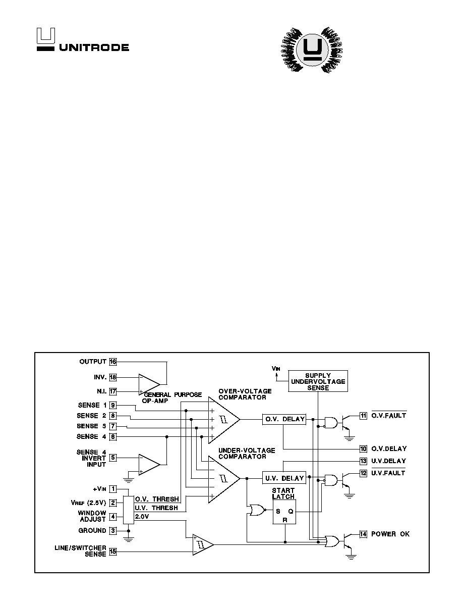
BLOCK DIAGRAM
4/97
Note: Pin numbers refer to J, N and DW packages.
UC1903
UC2903
UC3903
Supply Voltage (+V
IN
). . . . . . . . . . . . . . . . . . . . . . . . . . . . . +40V
Open Collector Output Voltages. . . . . . . . . . . . . . . . . . . . . +40V
Open Collector Output Currents . . . . . . . . . . . . . . . . . . . . 50mA
Sense 1-4 Input Voltages . . . . . . . . . . . . . . . . . . . -0.3V to +20V
Line/Switcher Sense Input Voltage . . . . . . . . . . . -0.3V to +40V
Op-Amp and Inverter Input Voltages . . . . . . . . . . -0.3V to +40V
Op-Amp and Inverter Output Currents . . . . . . . . . . . . . . -40mA
Window Adjust Voltage. . . . . . . . . . . . . . . . . . . . . 0.0V to +10V
Delay Pin Voltages . . . . . . . . . . . . . . . . . . . . . . . . . 0.0V to +5V
Reference Output Current . . . . . . . . . . . . . . . . . . . . . . . -40mA
Power Dissipation at T
A
= 25∞C (Note 1) . . . . . . . . . . . 1000mW
Power Dissipation at T
C
= 25∞C (Note 1) . . . . . . . . . . . 2000mW
Operating Junction Temperature . . . . . . . . . . . -55∞C to +150∞C
Storage Temperature . . . . . . . . . . . . . . . . . . . . -65∞C to +150∞C
Lead Temperature (Soldering, 10 Seconds) . . . . . . . . . . 300∞C
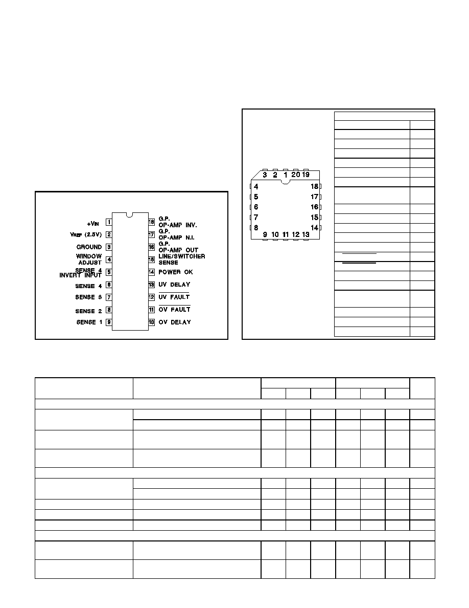
CONNECTION DIAGRAMS
DIL-18, SOIC-18 (TOP VIEW)
J or N, DW Package
PACKAGE PIN FUNCTION
FUNCTION
PIN
+VIN
1
V
REF
(2.5V)
2
GROUND
3
GROUND
4
WINDOW ADJUST
5
N/C
6
SENSE 4 INVERT
INPUT
7
SENSE 4
8
SENSE 3
9
SENSE 2
10
SENSE 1
11
OV DELAY
12
OV FAULT
13
UV FAULT
14
UV DELAY
15
POWER OK
16
LINE/SWITCHER
SENSE
17
G.P. OP-AMP OUT
18
G.P. OP-AMP N.I.
19
G.P. OP-AMP INV.
20
PLCC-20, LCC-20
(TOP VIEW)
Q, L Package
ELECTRICAL CHARACTERISTICS:
Unless otherwise stated, these specifications apply for T
A
= ≠55∞C to +125∞C for the
UC1903; ≠40∞C to +85∞C for the UC2903; and 0∞C to +70∞C for the UC3903; +V
IN
=
15V; Sense Inputs (Pins 6≠9 and Pin 15) = 2.5V; V
PIN 4
= 1.0V, T
A
= T
J.
PARAMETERS
TEST CONDITIONS
UC1903 / UC2903
UC3903
UNITS
MIN
TYP
MAX
MIN
TYP
MAX
Supply
Input Supply Current
No Faults
7
9
7
11
mA
UV, OV and Line Fault
10
15
10
18
mA
Supply Under Voltage
Threshold (V
SUV
)
Fault Outputs Enabled
6.0
7.0
7.5
5.5
7.0
8.0
V
Minimum Supply to Enable
Power OK Output
3.0
4.0
3.0
4.0
V
Reference
Output Voltage (V
REF
)
T
J
= 25∞C
2.485
2.5
2.515
2.470
2.5
2.530
V
Over Temperature
2.465
2.535
2.465
2.535
V
Load Regulation
I
L
= 0 to 10mA
1
10
1
15
mV
Line Regulation
+V
IN
= 8 to 40V
1
4
1
8
mV
Short Circuit Current
T
J
= 25∞C
40
40
mA
Fault Thresholds (Note 4)
OV Threshold Adj.
Offset from V
REF
as a function of V
PIN 4
Input = Low to High, 0.5V
V
PIN 4
2.5V
.230
.25
.270
.230
.25
.270
V/V
UV Threshold Adj.
Offset from V
REF
as a function of V
PIN 4
Input = High to Low, 0.5V
V
PIN 4
2.5V
-.270
-.25
-.230
-.270
-.25
-.230
V/V
ABSOLUTE MAXIMUM RATINGS (Note 1)
Note 1: Voltages are referenced to ground (Pin 3). Currents
are positive into, negative out of, the specified terminals.
Consult Packaging Section of Databook for thermal
limitations and considerations of package.
2
ELECTRICAL CHARACTERISTICS:
PARAMETERS
TEST CONDITIONS
UC1903/UC2903
UC3903
UNITS
MIN
TYP
MAX
MIN
TYP
MAX
Fault Thresholds (cont.)
OV & UV Threshold Hyst.
0.5V
V
PIN 4
2.5V
10
20
30
10
20
30
mV/V
OV & UV Threshold Supply
Sensitivity
+V
IN
= 8V to 40V
.002
.01
.002
.02
%/V
Adjust Pin (Pin 4)
Input Bias Current
0.5V
V
PIN 4
2.5V
±
1
±
10
±
1
±
12
µ
A/V
Line Sense Threshold
Input = High to Low
1.94
2.0
2.06
1.9
2.0
2.1
V
Line Sense Threshold Hyst.
125
175
225
100
175
250
mV
Sense Inputs
Sense 1-4
Input Bias Current
Input = 2.8V (Note 2)
1
3
1
6
µ
A
Input = 2.2 (Note 2)
-1
-3
-1
-6
µ
A
Line Sense Input
Bias Current
Input = 2.3V (Note 2)
1
3
1
6
µ
A
OV and UV Fault Delay
Charging Current
60
60
µ
A
Threshold Voltage
Delay Pin = Low to High
1.8
1.8
V
Threshold Hysteresis
T
J
= 25∞C
250
250
mV
Delay
Ratio of Threshold Voltage to Charging
Current
20
30
50
20
30
50
ms/
µ
F
Fault Outputs (OV, UV, & Power 0K)
Maximum Current
V
OUT
= 2V
30
70
30
70
mA
Saturation Voltage
I
OUT
= 12mA
.25
.40
.25
.40
V
Leakage Current
V
OUT
= 40 V
3
25
3
25
µ
A
Sense 4 Inverter (Note 3)
Input Offset Voltage
2
8
2
10
mV
Input Bias Current
.1
2
.1
4
µ
A
Open Loop Gain
65
80
65
80
dB
PSRR
+V
IN
= 8 to 40 V
65
100
65
100
dB
Unity Gain Frequency
1
1
MHz
Slew Rate
.4
.4
V/
µ
s
Short Circuit Current
T
J
= 25∞C
40
40
mA
G.P. Op-Amp (Note 3)
Input Offset Voltage
1
5
1
8
mV
Input Bias Voltage
.1
2
.1
4
µ
A
Input Offset Current
.01
.5
.01
1.0
µ
A
Open Loop Gain
65
120
65
120
dB
CMRR
V
CM
= 0 to +V
IN
= 2.0V
65
100
65
100
dB
PSRR
+V
IN
= 8 to 40V
65
100
65
100
dB
Unity Gain Frequency
1
1
MHz
Slew Rate
.4
.4
V/
µ
s
Short Circuit Current
T
J
= 25∞C
40
40
mA
Note 2: These currents represent maximum input bias currents required as the sense inputs cross appropriate thresholds.
Note 3: When either the G.P. OP-Amp, or the Sense 4 Inverter, are configured for sensing a negative supply voltage, the divider
resistance at the inverting input should be chosen such that the nominal divider current is
1.4mA. With the divider current
at or below this level possible latching of the circuit is avoided. Proper operation for currents at or below 1.4mA is 100%
tested in production.
Note 4: Reference to pin numbers in this specification pertain to 18 pin DIL N and J packages and 18 pin SOIC DW package.
UC1903
UC2903
UC3903
Unless otherwise stated, these specifications apply for T
A
= ≠55∞C to +125∞C for the
UC1903; ≠40∞C to +85∞C for the UC2903; and 0∞C to +70∞C for the UC3903; +V
IN
=
15V; Sense Inputs (Pins 6≠9 and Pin 15) = 2.5V; V
PIN 4
= 1.0V, T
A
= T
J.
3
UC1903
UC2903
UC3903
Typical 2.5V Reference
Temperature Characteristic
Typical Fault Delay
Temperature Characteristic (C
DELAY
270pF)
OPERATION AND APPLICATION INFORMATION
Figure 1. The UC1903 fault window circuitry generates OV and UV thresholds centered around the 2.5V reference.
Window magnitude and threshold hysteresis are proportional to the window adjust input voltage at Pin 4.
4

Setting a Fault Window
The fault thresholds on the UC1903 are generated by cre-
ating positive and negative offsets, equal in magnitude,
that are referenced to the chip's 2.5V reference. The re-
sulting fault window is centered around 2.5V and has a
magnitude equal to that of the applied offsets. Simplified
schematics of the fault window and reference circuits are
shown in Figure 1 (see previous page). The magnitude of
the offsets is determined by the voltage applied at the
window adjust pin, Pin 4. A bias cancellation circuit keeps
the input current required at Pin 4 low, allowing the use of
a simple resistive divider off the reference to set the ad-
just pin voltage.
The adjust voltage at Pin 4 is internally applied across R
4
,
and an 8k resistor. The resulting current is mirrored four
times to generate current sources I
OA
, I
OB
, I
OC
, and I
OD
,
all equal in magnitude. When all four of the sense inputs
are inside the fault window, a no-fault condition, Q
4
and
Q
5
are turned on. In combination with D
1
and D
2
this pre-
vents L
OB
and L
OD
from affecting the fault thresholds. In
this case, the OV and UV thresholds are equal to V
REF
+
I
OA
(R
5
+ R
6
) and V
REF
- I
OC
(R
7
+ R
8
) respectively. The
fault window can be expressed as:
(1) 2.5V
±
V
ADJ
4
.
In terms of a sensed nominal voltage level, V
S,
the win-
dow as a percent variation is:
(2) V
S
±
(
10
V
ADJ
)
%.
When a sense input moves outside the fault window given
in equation(1), the appropriate hysteresis control signal
turns off Q
4
or Q
5
. For the under-voltage case, Q
5
is dis-
abled and current source I
OB
flows through D
2
. The net
current through R
7
becomes zero as I
OB
cancels I
OC
, giv-
ing an 8% reduction in the UV threshold offset. The over-
voltage case is the same, with Q
4
turning off, allowing I
OD
to cancel the current flow, I
OA
, through R
6
. The result is a
UC1903
UC2903
UC3903
Figure 2.
The fault window and threshold hysteresis scale as a
function of the voltage applied at Pin 4, the window adjust pin.
Figure 4.
The general purpose op-amp on the UC1903 can be
used to create a sense input with an independently tighter fault
window.
Figure 3.
Using the reference output and a resistive divider, a
sense input with an independently wider fault window can be
generated.
Figure 4 demonstrates one of many auxiliary functions
that the uncommitted op-amp on the UC1903 can be
used for. Alternatively, this op-amp can be used to buffer
high impedance points, perform logic functions, or for
sensing and amplification. For example, the G.P. op-amp,
combined with the 2.5V reference, can be used to pro-
duce and buffer an optically coupled feedback signal in
isolated supplies with primary side control. The output
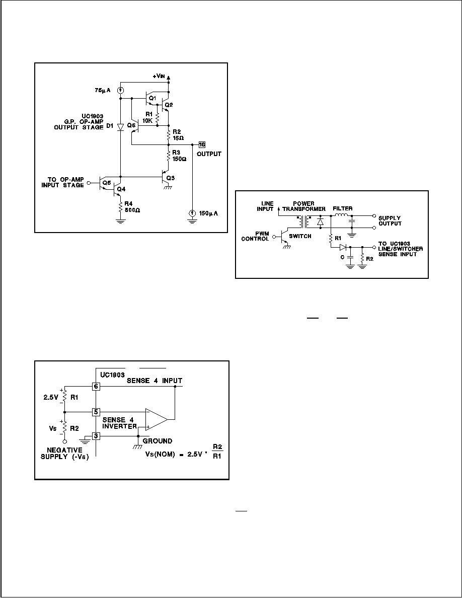
stage of this op-amp is detailed in Figure 5. The NPN
emitter follower provides high source current capability.
20mA while the substrate device, Q
3
, provides good
transient sinking capability.
Fault window for the Sense Input,
in percent, is:
±
10 (V
ADJ
)
∑
R
3
+
R
1
R
2
/
(
R
1
+
R
2
)
R
3
,
for:
V
S
(
NOM
)
∑
R
2
R
1
+
R
2
= 2.5V
Fault window for the sense input, in percent, is:
±
10 (V
ADJ
)
∑
R
2
R
1
+
R
2
OPERATION AND APPLICATION INFORMATION
hysteresis at the sense inputs which is always 8% of the
window magnitude. This is shown graphically in Figure 2.
Fault Windows Can Be Scaled Independently
In many applications, it may be desirable to monitor vari-
ous supply voltages, or voltage levels, with varying fault
windows. Using the reference output and external resis-
tive dividers this is easily accomplished with the UC1903.
Figures 3 and 4 illustrate how the fault window at any
sense input can be scaled independently of the remaining
inputs.
5
UC1903
UC2903
UC3903
Sensing a Negative Voltage Level
The UC1903 has a dedicated inverter coupled to the
sense 4 input. With this inverter, a negative voltage level
can be sensed as shown in Figure 6. The output of the in-
verter is an unbiased emitter follower. By tying the invert-
ing input, Pin 5, high the output emitter follower will be
reverse biased, leaving the sense 4 input in a high imped-
ance state. In this manner, the sense 4 input can be used,
as the remaining sense inputs would be, for sensing posi-
tive voltage levels.
Using The Line/Switcher Sense Output
The line switcher sense input to the UC1903 can be used
for early detection of line, switcher, or other power source,
failures. Internally referenced to 2.0V, the line sense com-
parator will cause the POWER OK output to indicate a
fault (active low) condition when the LINE/SWITCHER
SENSE input goes from above to below 2.0V. The line
sense comparator has approximately 175mV of hystere-
sis requiring the line/switcher input to reach 2.175V be-
fore the POWER OK output device can be turned off,
allowing a no-fault indication. In Figure 7 an example
showing the use of the LINE/SWITCHER SENSE input
for early switcher-fault detection is detailed. A sample sig-
nal is taken from the output of the power transformer, rec-
tified and filtered, and used at the line/switcher input. By
adjusting the R
2
C time constant with respect to the
switching frequency of the supply and the hold up time of
the output capacitor, switcher faults can be detected be-
fore supply outputs are significantly affected.
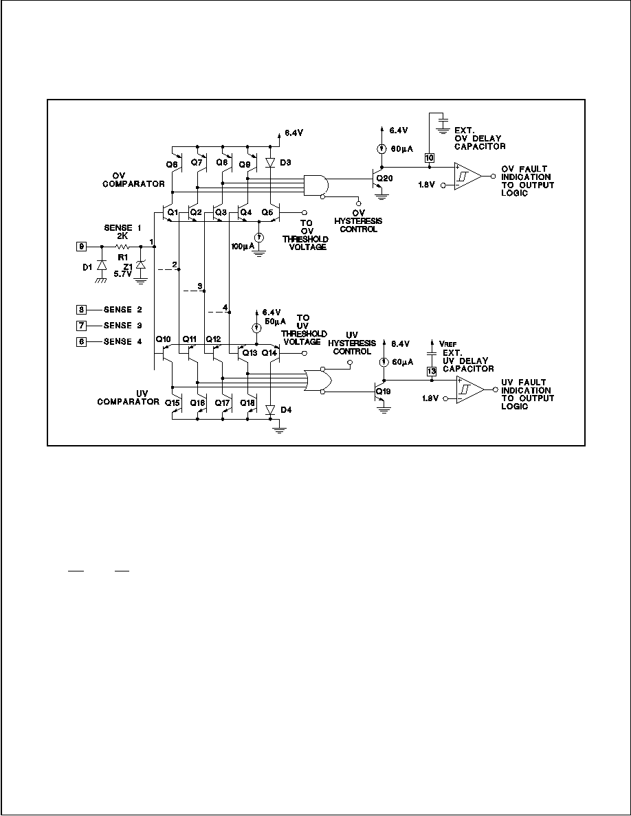
OV and UV Comparators Maintain Accurate
Thresholds
The structure of the OV and UV comparators, shown in
Figure 8 results in accurate fault thresholds even in the
case where multiple sense inputs cross a fault threshold
simultaneously. Unused sense inputs can be tied either to
the 2.5V reference, or to another, utilized, sense input.
The four under- and over-voltage sense inputs on the
UC1903 are clamped as detailed on the Sense 1 input in
Figure 8. The series 2k resistor, R
1
, and zener diode Z
1
,
prevent extreme under- and over-voltage conditions from
inverting the outputs of the fault comparators. A parasitic
diode, D
1
, is present at the inputs as well. Under normal
operation it is advisable to insure that voltage levels at all
of the sense inputs stay above -0.3V. The same type of
input protection exists at the line sense input, Pin 15, ex-
cept a 5k series resistor is used.
The fault delay circuitry on the UC1903 is also shown in
Figure 8. In the case of an over-voltage condition at one
of the sense inputs Q
20
is turned off, allowing the internal
60
µ
A current source to charge the user-selected delay
capacitor. When the capacitor voltage reaches 1.8V, the
OV and POWER OK outputs become active low. When
the fault condition goes away Q
20
is turned back on, rap-
idly discharging the delay capacitor. Operation of the un-
der-voltage delay is, with appropriate substitutions, the
same.
Figure 5.
The G.P. op-amp on the UC1903 has a high source
current (
20mA) capability and enhanced transient sinking capa-
bility through substrate device Q
3
.
Figure 7.
The line/switcher sense input can be used for an
early line or switcher fault indication.
Figure 6.
Inverting the sense 4 input for monitoring a negative
supply is accommodated with the dedicated inverter.
Note: A similar scheme w/the G.P. op-amp will allow a sec-
ond negative supply to be monitored.
OPERATION AND APPLICATION INFORMATION (continued)
6
UC1903
UC2903
UC3903
OPERATION AND APPLICATION INFORMATION (continued)
UNITRODE CORPORATION
7 CONTINENTAL BLVD.
∑
MERRIMACK, NH 03054
TEL. (603) 424-2410
∑
FAX (603) 424-3460
Start Latch and Supply Under-Voltage Sense Allow
Predictable Power-Up
The supply under-voltage sense and start-latch circuitry
on the UC1903 prevents fault indications during start-up
or low input supply (+V
IN
) conditions. When the input sup-
ply voltage is below the supply under-voltage threshold
the OV and UV fault outputs are disabled and the
POWER OK output is active low. The POWER OK output
will remain active until the input supply drops below ap-
proximately 3.0V. With +V
IN
below this level, all of the
open collector outputs will be off.
When the input supply is low, the under-voltage sense cir-
cuitry resets the start-latch. With the start-latch reset, the
UV fault output will remain disabled until the input supply
rises to its normal operating level (8-40V), and all of the
sense inputs are above the under-voltage threshold. This
allows slow starting, or supply sequencing, without an ar-
tificial under-voltage fault indication. Once the latch is set,
the UV fault output will respond if any of the sense inputs
drop below the under-voltage threshold.
Figure 8.
The OV and UV comparators on the UC1903 trigger respective fault delay circuits when one or more of the sense inputs
move outside the fault window. Input clamps insure proper operation under extreme fault conditions. Terminating the UV delay ca-
pacitor to V
REF
assures correct logic at power up.
7

IMPORTANT NOTICE
Texas Instruments and its subsidiaries (TI) reserve the right to make changes to their products or to discontinue
any product or service without notice, and advise customers to obtain the latest version of relevant information
to verify, before placing orders, that information being relied on is current and complete. All products are sold
subject to the terms and conditions of sale supplied at the time of order acknowledgement, including those
pertaining to warranty, patent infringement, and limitation of liability.
TI warrants performance of its semiconductor products to the specifications applicable at the time of sale in
accordance with TI's standard warranty. Testing and other quality control techniques are utilized to the extent
TI deems necessary to support this warranty. Specific testing of all parameters of each device is not necessarily
performed, except those mandated by government requirements.
CERTAIN APPLICATIONS USING SEMICONDUCTOR PRODUCTS MAY INVOLVE POTENTIAL RISKS OF
DEATH, PERSONAL INJURY, OR SEVERE PROPERTY OR ENVIRONMENTAL DAMAGE ("CRITICAL
APPLICATIONS"). TI SEMICONDUCTOR PRODUCTS ARE NOT DESIGNED, AUTHORIZED, OR
WARRANTED TO BE SUITABLE FOR USE IN LIFE-SUPPORT DEVICES OR SYSTEMS OR OTHER
CRITICAL APPLICATIONS. INCLUSION OF TI PRODUCTS IN SUCH APPLICATIONS IS UNDERSTOOD TO
BE FULLY AT THE CUSTOMER'S RISK.
In order to minimize risks associated with the customer's applications, adequate design and operating
safeguards must be provided by the customer to minimize inherent or procedural hazards.
TI assumes no liability for applications assistance or customer product design. TI does not warrant or represent
that any license, either express or implied, is granted under any patent right, copyright, mask work right, or other
intellectual property right of TI covering or relating to any combination, machine, or process in which such
semiconductor products or services might be or are used. TI's publication of information regarding any third
party's products or services does not constitute TI's approval, warranty or endorsement thereof.
Copyright
©
1999, Texas Instruments Incorporated