 | –≠–ª–µ–∫—Ç—Ä–æ–Ω–Ω—ã–π –∫–æ–º–ø–æ–Ω–µ–Ω—Ç: UC2907DW | –°–∫–∞—á–∞—Ç—å:  PDF PDF  ZIP ZIP |
UC1907, UC2907, UC3907
LOAD SHARE CONTROLLER
SLUS165C ≠ MARCH 1999 - REVISED JANUARY 2002
1
www.ti.com
FEATURES
D
Fully Differential High Impedance Voltage
Sensing
D
Accurate Current Amplifier for Precise
Current Sharing
D
Opto Coupler Driving Capability
D
1.25% Trimmed Reference
D
Master Status Indication
D
4.5-V to 35-V Operation
DESCRIPTION
The UCx907 family of load share controller ICs provides all the necessary features to allow
multiple-independent-power modules to be paralleled such that each module supplies only its proportionate share
to total-load current.
This sharing is accomplished by controlling each module's power stage with a command generated from a
voltage-feedback amplifier whose reference can be independently adjusted in response to a common-share-bus
voltage. By monitoring the current from each module, the current share bus circuitry determines which paralleled
module would normally have the highest output current and, with the designation of this unit as the master, adjusts
all the other modules to increase their output current to within 2.5% of that of the master.
The current share bus signal interconnecting all the paralleled modules is a low-impedance, noise-insensitive line
which will not interfere with allowing each module to act independently should the bus become open or shorted to
ground. The UC3907 controller will reside on the output side of each power module and its overall function is to supply
a voltage feedback loop. The specific architecture of the power stage is unimportant. Either switching or linear designs
may be utilized and the control signal may be either directly coupled or isolated though the use of an optocoupler or
other isolated medium.
Other features of the UC3907 include 1.25% accurate reference: a low-loss, fixed-gain current-sense amplifier, a fully
differential, high-impedance voltage sensing capability, and a status indicator to designate which module is
performing as master.
Copyright
2000, Texas Instruments Incorporated
PRODUCTION DATA information is current as of publication date.
Products conform to specifications per the terms of Texas Instruments
standard warranty. Production processing does not necessarily include
testing of all parameters.
Please be aware that an important notice concerning availability, standard warranty, and use in critical applications of
Texas Instruments semiconductor products and disclaimers thereto appears at the end of this data sheet.
1
2
3
4
5
6
7
8
16
15
14
13
12
11
10
9
C/S OUT
C/S (+)
C/S (≠)
(≠) SENSE
POWER RETURN
ARTIFICIAL GND
VREF
ISET
STATUS INDICATE
CURRENT SHARE BUS
ADJ OUT
ADJ INPUT
COMP
(+) SENSE
VCC
OPTO DRIVE
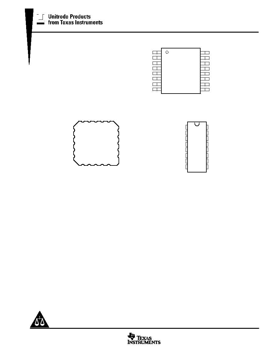
DIL-16 J or N PACKAGE
(TOP VIEW)
1
2
3
4
5
6
7
8
16
15
14
13
12
11
10
9
C/S OUT
C/S (+)
C/S (≠)
(≠) SENSE
POWER RETURN
ARTIFICIAL GND
VREF
ISET
STATUS INDICATE
CURRENT SHARE BUS
ADJ OUT
ADJ INPUT
COMP
(+) SENSE
VCC
OPTO DRIVE
SOIC-16 DW PACKAGE
(TOP VIEW)
19
20
1
3
2
17
18
16
15
14
13
12
11
9
10
5
4
6
7
8
ADJ OUT
ADJ INPUT
N/C
COMP
(+) SENSE
C/S (≠)
(≠) SENSE
N/C
POWER RETURN
ARTIFICIAL GND
C/S (+)
C/S OUT
N/C
ST
A
TUS INDICA
TE
CURRENT
SHARE BUS
ISET
N/C
OPT
O DRIVE
VCC
VREF
PLCC-20, LCC-20,
Q OR L PACKAGE
(TOP VIEW)
UC1907, UC2907, UC3907
LOAD SHARE CONTROLLER
SLUS165C ≠ MARCH 1999 - REVISED JANUARY 2002
2
www.ti.com
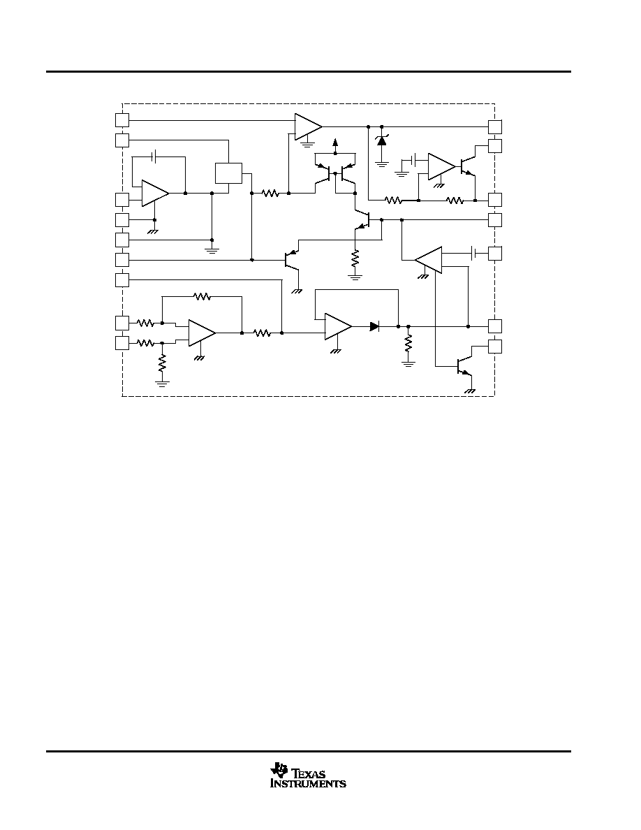
block diagram
11
14
10
13
8
9
12
15
16
7
5
4
1
6
3
2
2 k
2 k
+
≠
40 k
40 k
CURRENT SENSE
AMPLIFIER
100
+
≠
BUFFER
AMPLIFIER
+
≠
+
50 mV
ADJUST
AMPLIFIER
ADJ
V
CC
1 k
V
REF
1.75 V
+
≠
+
GROUND
AMPLIFIER
0.25 V
GND
+
≠
50 k
20 k
+
1.0 V
1.75 V
VOLTAGE ERROR AMPLIFIER
STATUS INDICATE
CURRENT SHARE BUS
ADJ INPUT
ADJ OUT
ISET
OPTO DRIVE
COMP
(+) SENSE
VCC (4.5 V TO 35 V)
(≠) SENSE
POWER RTN
ARTIFICIAL GND
VREF
C/S OUT
C/S (≠)
C/S (+)
DRIVE
AMPLIFIER
+
≠
DRV
10 k
17.5 k
absolute maximum ratings over operating free-air temperature (unless otherwise noted)
Supply voltage
35 V
. . . . . . . . . . . . . . . . . . . . . . . . . . . . . . . . . . . . . . . . . . . . . . . . . . . . . . . . . . . . . . . . . . . . . . . . . . . . .
Opto out voltage
35 V
. . . . . . . . . . . . . . . . . . . . . . . . . . . . . . . . . . . . . . . . . . . . . . . . . . . . . . . . . . . . . . . . . . . . . . . . . . .
Opto out current
20 mA
. . . . . . . . . . . . . . . . . . . . . . . . . . . . . . . . . . . . . . . . . . . . . . . . . . . . . . . . . . . . . . . . . . . . . . . . . . .
Status indicate sink current
20 mA
. . . . . . . . . . . . . . . . . . . . . . . . . . . . . . . . . . . . . . . . . . . . . . . . . . . . . . . . . . . . . . . . .
C/S input voltage
35 V
. . . . . . . . . . . . . . . . . . . . . . . . . . . . . . . . . . . . . . . . . . . . . . . . . . . . . . . . . . . . . . . . . . . . . . . . . . .
Share bus voltage
≠0.3 V to 35 V
. . . . . . . . . . . . . . . . . . . . . . . . . . . . . . . . . . . . . . . . . . . . . . . . . . . . . . . . . . . . . . . . . .
Other analog inputs and outputs (zener clamped) maximum forced voltage
≠0.3 V to10 V
. . . . . . . . . . . . . . . .
Other analog inputs and outputs (zener clamped) maximum forced current
±
10 mA
. . . . . . . . . . . . . . . . . . . . .
Ground amp sink current
50 mA
. . . . . . . . . . . . . . . . . . . . . . . . . . . . . . . . . . . . . . . . . . . . . . . . . . . . . . . . . . . . . . . . . . .
Pins 1, 9, 12, 15 sink current
20 mA
. . . . . . . . . . . . . . . . . . . . . . . . . . . . . . . . . . . . . . . . . . . . . . . . . . . . . . . . . . . . . . . .
Storage temperature range, T
stg
≠65
∞
C to 150
∞
C
. . . . . . . . . . . . . . . . . . . . . . . . . . . . . . . . . . . . . . . . . . . . . . . . . . .
Junction temperature, T
J
≠55
∞
C to 150
∞
C
. . . . . . . . . . . . . . . . . . . . . . . . . . . . . . . . . . . . . . . . . . . . . . . . . . . . . . . . . .
Lead temperature (solder 10 seconds)
300
∞
C
. . . . . . . . . . . . . . . . . . . . . . . . . . . . . . . . . . . . . . . . . . . . . . . . . . . . . . .
Pin Nos. refer to 16 Pin DIL Package.
Currents are positive into, negative out of the specified terminal. Consult packaging section of databook for thermal limitations and considerations
of package.
UC1907, UC2907, UC3907
LOAD SHARE CONTROLLER
SLUS165C ≠ MARCH 1999 - REVISED JANUARY 2002
3
www.ti.com
electrical characteristics, these specifications apply for T
A
= ≠55
∞
C to 125
∞
C for UC1907, ≠40
∞
C to
85
∞
C for UC2907, and 0
∞
C to 70
∞
C for UC3907, V
IN
= 15 V, T
A
= T
J
(unless otherwise stated )
PARAMETER
TEST CONDITIONS
MIN
TYP
MAX
UNITS
Voltage Amp Section
Inp t oltage
COMP = 1 V,
TA = 25
∞
C
1.975
2.000
2.025
V
Input voltage
COMP = 1 V,
over temp
1.960
2.000
2.040
V
Line regulation
VIN = 4.5 V to 35 V
15
mV
Load regulation
IL reference = 0.0 mA to ≠10 mA
10
mV
Long term stability
TA = 125
∞
C,
1000hrs See Note 2
5
25
mV
Total output variation
Line, load, temp
1.960
2.040
Input adjust range
ADJ OUT from max high to max low
85
100
115
mV
Input bias current
≠1
µ
A
Open loop gain
COMP = 0.75 V to 1.5 V
65
dB
Unity gain bandwidth
TA = 25
∞
C
See Note 2
700
kHz
Output sink current
(+) SENSE = 2.2 V,
COMP = 1 V
6
15
mA
Output source current
(+) SENSE = 1.8 V,
COMP = 1 V
400
600
µ
A
VOUT high
(+) SENSE = 1.8 V,
IL = ≠400
µ
1.85
2
V
VOUT low
(+) SENSE = 2.2 V,
IL = 1 mA
0.15
0.40
V
Reference Section
O tp t oltage
TA = 25
∞
C
1.970
2.000
2.030
V
Output voltage
Over operating temp
1.955
2.000
2.045
V
Short circuit current
VREF = 0.0 V
≠15
≠30
≠60
mA
Ground Amp Section
Output voltage
200
250
300
mV
Common mode variation
(≠) SENSE from 0.0 V to 2 V
5
mV
Load reg lation
IL = 0.0 mA to 20 mA,
TA = 25
∞
C
10
mV
Load regulation
IL = 0.0 mA to 20 mA,
over temp
15
mV
Adjust Amp Section
Input offset voltage
ADJ OUT = 1.5 V, VCM = 0.0 V
40
50
60
mV
Input bias current
≠2
µ
A
Open loop gain
1.5 V
ADJ OUT
2.25 V
65
dB
Unity gain bandwidth
TA = 25
∞
C, COUT =1
µ
F
See Note 2
500
Hz
Transconductance
IOUT = ≠10
µ
A to 10
µ
A, VOUT = 1.5 V
1.7
3
4.5
ms
Output sink current
VID = 0.0 V,
ADJ OUT = 1.5 V
55
135
225
µ
A
Output source current
VID = 250 mV,
ADJ OUT = 1.5 V
110
200
350
µ
A
VOUT high
VID = 250 mV,
IOUT = ≠ 50 mA
2.20
2.70
2.90
V
VOUT low
VID = 0.0 V,
IOUT = 50 mA
0.75
1.15
V
Common mode rejection ratio
VCM = 0.0 to 10 V
70
dB
Output gain to V/A
VOUT ADJ OUT = 1.5 V to 2 V,
(+) SENSE/
ADJ OUT
50
57
64
mV/V
NOTE 1: Unless otherwise specified all voltages are with respect to (≠) SENSE. Currents are positive into, negative out of the specified terminal.
NOTE 2: Ensured by design. Not production tested.
UC1907, UC2907, UC3907
LOAD SHARE CONTROLLER
SLUS165C ≠ MARCH 1999 - REVISED JANUARY 2002
4
www.ti.com
electrical characteristics, these specifications apply for T
A
= ≠55
∞
C to 125
∞
C for UC1907, ≠40
∞
C to
85
∞
C for UC2907, and 0
∞
C to 70
∞
C for UC3907, V
IN
= 15 V, T
A
= T
J
(unless otherwise stated )
PARAMETER
TEST CONDITIONS
MIN
TYP
MAX
UNITS
Current Amp Section
Gain
VCM = 0.0 V,
VID = 50 mV to 100 mV
19.2
19.6
20.1
V/V
O tp t oltage
VC/S (+) = VC/S (≠) = 0.0 V, TA = 25
∞
C
210
250
290
mV
Output voltage
VC/S (+) = VC/S (≠) = 0.0 V, over temp
180
250
330
mV
Input offset change with common mode
input
VCM = 0 V to 13 V
600
µ
V/V
VOUT high
VID = 1 V
10
14.5
V
VOUT low
VID = ≠ 1 V,
IL = 1 mA
350
450
mV
Power supply rejection ratio
VIN = 4.5 V to 35 V,
VCM = 0.0 V
60
dB
Slew rate
0.4
V/
µ
s
Drive Amp Section RSET = 500
to Artificial GND, Opto Drive = 15 V
Voltage gain
COMP = 0.5 V to 1 V
2.3
2.5
2.6
V/V
ISET VOUT high
(+) SENSE = 2.2 V
3.8
4.1
4.4
V
ISET VOUT low
(+) SENSE = 1.8 V
270
300
mV
Opto out voltage range
4
35
V
Zero current input threshold
1.55
1.65
1.75
V
Buffer Amp Section
Input offset voltage
Input = 1 V
5
mV
Output off impedance
Input = 1 V,
output = 1.5 V to 2 V
5
10
20
k
Output source current
Input = 1 V,
output = 0.5 V
6
15
mA
Common mode rejection ratio
VCM = 0.3 V to 10 V
70
dB
Power supply rejection ratio
VIN = 4.5 V to 35 V
70
dB
Under Voltage Lockout Section
Startup threshold
3.7
4.4
V
Threshold hysteresis
200
mV
Status Indicate Section
VOUT low
ADJ OUT = current share bus
0.2
0.5
V
Output leakage
ADJ OUT = 1 V,
VOUT = 35 V
0.1
5
µ
A
Total Stand by Current Section
Startup current
VIN = UVLO ≠ 0.2 V
3
5
mA
Operating current
VIN = 35 V
6
10
mA
NOTE 1: Unless otherwise specified all voltages are with respect to (≠) SENSE. Currents are positive into, negative out of the specified terminal.
NOTE 2: Ensured by design. Not production tested.

UC1907, UC2907, UC3907
LOAD SHARE CONTROLLER
SLUS165C ≠ MARCH 1999 - REVISED JANUARY 2002
5
www.ti.com
pin assignments
(≠) SENSE: (Pin 4) This is a high-impedance pin allowing remote sensing of the system ground, bypassing any
voltage drops which might appear in the power return line. This point should be considered as the true ground. Unless
otherwise stated, all voltages are with respect to this point.
Artificial Ground: (Pin 6) This is a low-impedance-circuit ground which is exactly 250 mV above the (≠) SENSE
terminal. This offset allows the ground buffer amplifier negative headroom to return all the control bias and operating
currents while maintaining a high impedance at the (≠) SENSE input.
Power RTN: (Pin 5) This should be the most negative voltage available and can range from zero to 5 V below the
(≠) SENSE terminal. It should be connected as close to the power source as possible so that voltage drops across
the return line and current-sensing impedances lie between this terminal and the (≠) SENSE point.
VREF: (Pin 7) The internal voltage reference is a band-gap circuit set at 2.0 V with respect to the (≠) SENSE input
(1.75 V above the artificial ground), and an accuracy of
±
1.5%. This circuit, as well as all the other chip functions, will
work over a supply voltage range of 4.5 V to 35 V allowing operation from unregulated dc, an auxiliary voltage, or
the same output voltage that it is controlling. Under-voltage lockout has been included to insure proper startup by
disabling internal bias currents until the reference rises into regulation.
Voltage Amplifier: (Pins 11, 12) This circuit is the feedback-control-gain stage for the power module's output-voltage
regulation, and overall-loop compensation will normally be applied around this amplifier. Its output will swing from
slightly above the ground return to an internal clamp of 2.0 V. The reference trimming is performed closed loop, and
measured at pin 11, (+) SENSE. The value is trimmed to 2 V
±
1.25%.
Drive Amplifier: (Pins 8, 9, 12) This amplifier is used as an inverting buffer between the voltage amplifier's output
and the medium used to couple the feedback signal to the power controller. It has a fixed-voltage gain of 2.5 and is
usually configured with a current-setting resistor to ground. This establishes a current-sinking output optimized to
drive optical couplers biased at any voltage from 4.5 V to 35 V, with current levels up to 20 mA. The polarity of this
stage is such that an increasing voltage at the voltage amplifier's sense input (as, for example, at turnon) will increase
the opto's current. In a nonisolated application, a voltage signal ranging from 0.25 V to 4.1 V may be taken from the
current-setting output but it should be noted that this voltage will also increase with increasing sense voltage and an
external inverter may be required to obtain the correct feedback polarity.
Current Amplifier: (Pins 1, 2, 3) This amplifier has differential-sensing capability for use with an external shunt in
the power-return line. The common mode range of its input will accommodate the full range between the power return
point and VCC-2 V which will allow undefined-line impedances on either side of the current shunt. The gain is
internally set at 20, giving the user the ability to establish the maximum-voltage drop across the current-sense resistor
at any value between 50 mV and 500 mV. While the bandwidth of this amplifier may be reduced with the addition of
an external-output capacitor to ground, in most cases this is not required as the compensation of the adjust amplifier
will typically form the dominant pole in the adjust loop.
Buffer Amplifier: (Pins 1, 15) This amplifier is a unidirectional buffer which drives the current-share bus. The line
which will interconnect all power modules paralleled for current sharing. Since the buffer amplifier will only source
current, it insures that the module with the highest-output current will be the master and drive the bus with a
low-impedance drive capability. All other buffer amplifiers will be inactive with each exhibiting a 10-k
load impedance
to ground. The share bus terminal is protected against both shorts to ground and accidental voltages in excess of
50 V.