 | –≠–ª–µ–∫—Ç—Ä–æ–Ω–Ω—ã–π –∫–æ–º–ø–æ–Ω–µ–Ω—Ç: UC29431 | –°–∫–∞—á–∞—Ç—å:  PDF PDF  ZIP ZIP |

UC19431
UC29431
UC39431
UC39431B
DESCRIPTION
The UC39431 is an adjustable shunt voltage regulator with 100mA sink ca-
pability.
The
architecture,
comprised
of
an
error
amplifier
and
transconductance amplifier, gives the user separate control of the small
signal error voltage frequency response along with a fixed linear
transconductance. A minimum 3MHz gain bandwidth product for both the
error and transconductance amplifiers assures fast response. In addition to
external programming, the IC has three internal resistors that can be con-
nected in six different configurations to provide regulated voltages of 2.82V,
3.12V, 5.1V, 7.8V, 10.42V, and 12.24V. A sister device (UC39432) provides
access to the non-inverting error ampilifer input and reference, while elimi-
nating the three internal resistors.
Precision Adjustable Shunt Regulator
FEATURES
∑
Multiple On-Chip Programmable
Reference Voltages
∑
0.4% Initial Accuracy
∑
0.7% Overall Reference Tolerance
∑
2.2V to 36.0V Operating Supply
Voltage and User Programmable
Reference
∑
36.0V Operating Supply Voltage
∑
Reference Accuracy Maintained For
Entire Range of Supply Voltage
∑
Superior Accuracy and Easier
Compensation for Optoisolator
Application
∑
Improved Architecture Provides a
Known Linear Transconductance with
a +5% Typical Tolerance
04/99
BLOCK DIAGRAM
UDG-95087

2
UC19431
UC29431
UC39431
UC39431B
DIL-8, SOIC-8 (Top View)
N or J, D Package
ABSOLUTE MAXIMUM RATINGS
Supply Voltage: V
. . . . . . . . . . . . . . . . . . . . . . . . . . . . . 36V
Regulated Output: V . . . . . . . . . . . . . . . . . . . . . . . . . . . . . . 36V
Internal Resistors: R1, R2, R3 . . . . . . . . . . . . . . . . . . . . . . . 13V
E/A Input: SENSE . . . . . . . . . . . . . . . . . . . . . . . . . . . . . . . . . 6V
E/A Compensation: COMP . . . . . . . . . . . . . . . . . . . . . . . . . . 6V
Output Sink Current: I . . . . . . . . . . . . . . . . . . . . . . . . . . . 140mA
Power Dissipation at T
A
25∞C (DIL-8) . . . . . . . . . . . . . . . . . 1W
Derate 8mW/∞C for T
A
> 25∞C
Storage Temperature Range . . . . . . . . . . . . . ≠65∞C to +150∞C
Junction Temperature . . . . . . . . . . . . . . . . . . . ≠55∞C to +150∞C
Lead Temperature (Soldering, 10 sec.) . . . . . . . . . . . . . +300∞C
Currents are positive into, negative out of the specified termi-
nal. Consult Packaging Section of Databook for thermal limita-
tions and considerations of packages.
ELECTRICAL CHARACTERISTICS:
Unless otherwise stated, these specifications apply for T
A
= ≠55∞C to +125∞C and
COLL Output = 2.4V to 36.0V for the UC19431, T
A
= ≠25∞C to +85∞C and COLL Output = 2.3V to 36.0V for the UC29431, and T
A
= 0∞C to +70∞C and COLL Output = 2.3V to 36.0V for the UC39431/B, VCC = 15V, I
COLL
= 10mA, T
A
= T
J
.
PARAMETER
TEST CONDITIONS
MIN
TYP
MAX
UNITS
Reference Voltage Tolerance
T
A
= 25∞C
19431*
1.295
1.3
1.305
V
39431B
1.29
1.3
1.31
V
Reference Temperature Tolerance
V
COLL
= 5.0
19431*
1.291
1.3
1.309
V
39431B
1.286
1.3
1.314
V
Reference Line Regulation
Reference Load Regulation
VCC = 2.2V to 36.0V, V
COLL
= 5V
I
COLL
= 10mA to 50mA, V
COLL
= 5V
19431*
10
38
mV
39431B
19431*
10
10
57
38
mV
mV
39431B
10
57
mV
Sense Input Current
≠0.5
≠0.2
µ
A
Minimum Operating Current
VCC = 36.0V, V
COLL
= 5V
0.50
0.80
mA
Collector Current Limit
V
COLL
= VCC = 36.0V, Ref = 1.35V
130
145
mA
Collector Saturation
I
COLL
= 20mA
0.7
1.1
1.5
V
Transconductance (gm)
VCC = 2.4V to 36.0V,
V
COLL
= 3V, I
COLL
= 20mA
19431*
≠170
≠140
≠110
mS
39431B
≠180
≠140
≠100
mS
5.1V Reference
Internal Divider
19431*
5.05
5.1
5.15
V
39431B
5
5.1
5.2
V
12.24V Reference
Internal Divider
19431*
12
12.24
12.5
V
39431B
12
12.24
12.5
V
Error Amplifier AVOL
60
90
dB
Error Amplifier GBW
(Note 1)
3.0
5
MHz
Transconductance Amplifier GBW
3
MHz
* Also applies to the UC29431 and UC39431
Note: The internal divider can be configured to give six unique references. These references are 2.82V, 3.12V, 5.1V, 7.8V,
10.42V, 12.24V.
Note 1: Guaranteed by design. Not 100% tested in production.
CONNECTION DIAGRAM

3
UC19431
UC29431
UC39431
UC39431B
COLL: The collector of the output transistor with a maxi-
mum voltage of 36V.
This pin is the output of the
transconductance amplifier. The overall open loop volt-
age gain of the transconductance amplifier is gm ∑ RL,
where gm is designed to be ≠140mS ±30mS and RL rep-
resents the output load.
COMP: The output of the error amplifier and the input to
the transconductance amplifier. This pin is available to
compensate the high frequency gain of the error ampli-
fier. It is internally voltage limited to approximately 2.0V.
GND: The reference and power ground for the device.
The power ground of the output transistor is isolated on
the chip from the substrate ground used to bias the re-
mainder of the device.
R1, R2, R3: Connection points to the three internal resis-
tors.
SENSE: The inverting terminal of the error amplifier used
as both the voltage sense input to the error amplifier and
its other compensation point. The error amplifier uses the
SENSE input to compare against the 1.3V on-chip refer-
ence.
The SENSE pin is also used as the undervoltage lockout
(UVLO). It is intended to keep the chip from operating un-
til the internal reference is properly biased. The thresh-
old is approximately 1V. It is important that once the
UVLO is released, the error amplifier can drive the
transconductance amplifier to stabilize the loop. If a ca-
pacitor is connected between the SENSE and COMP
pins to create a pole, it will limit the slew rate of the error
amplifier. To increase the bandwidth and ensure startup
at low load current, it is recommended to create a zero
along with the pole as shown in the shunt regulator appli-
cation. The error amplifier must slew 2.0V to drive the
transconductance amplifier initially on.
VCC: The power connection for the device. The minimum
to maximum operating voltage is 2.2V to 36.0V. The qui-
escent current is typically 0.50mA.
PIN DESCRIPTIONS (cont.)
Figure 1. Typical 5.1V shunt regulator application.
UDG-95088

4
UC19431
UC29431
UC39431
UC39431B
Magnetic Amplifier Controller Application
The 0.4% initial reference makes the UC39431 ideal as a
programmable shunt regulator. By adding two external
resistors, the on-chip 1.3V reference can be gained to
any voltage between 2.2V (2.4V for the UC39431) and
36.0V. The input bias current is typically maintained at
0.2µA
for
the
output
voltage
range.
Since
the
non-inverting error amplifier input is not available, a 5.1k
non-inverting input impedance is added to the input of
the error amplifier. This allows the user to choose the
SENSE pin input impedance to cancel the minimal offset
voltage caused by the input bias current.
Frequency Compensation
The UC39431 shunt regulator is designed with two
independant gain stages. The error amplifier provides
90dB of gain with a typical gain bandwidth product of
5MHz. The error amplifier provides sufficient gain in or-
der for the sense voltage to be accurately compared to
the 1.3V on-chip reference. Complete control of the fre-
quency response of the error amplifier is accomplished
with the COMP pin. By putting negative feedback across
the error amplifier, either a pole or a pole-zero can be
added.
The second gain stage is the transconductance (gm) am-
plifier. The gm amplifier is designed with a known linear
140mS of transconductance. The voltage gain is conse-
quently gm ∑ Ro, where Ro is the output impedance at
the collector pin. The frequency response of the
transconductance amplifier is controlled with the COLL
pin. The gain bandwidth product of the gm amplifier is
typically 3MHz. A pole or pole-zero can be added to this
stage by connecting a capacitor or a series capacitor and
resistor between COLL and GND.
The compensation of a control loop containing the
UC39431 is made easier due to the independant com-
pensation capability of the error amplifier and gm ampli-
fier. As shown in the applications information, a pole-zero
is created with a series resistor and capacitor between
SENSE and COMP. The pole created is dominant, while
the zero is used to increase the bandwidth and cancel
the effects of the pole created by the capacitor between
the COLL and GND pins.
APPLICATION INFORMATION
6
5
7
4
20k
4k
REF
2.85k
2
22.4k
16k
5.1
8
1
3
1.3V
0.5V
GND
COLL
I
COLL
40.2K
6.8nF
21K
V
SENSE
R1
R2
R3
SENSE
2K
COMP
VCC
Figure 2. 15.0V optocoupler application.
UDG-99051
5
UC19431
UC29431
UC39431
UC39431B
Optocoupler Application
The two amplifier circuit architecture employed in the
UC39431 is most advantageous for the optocoupler ap-
plication. The error amplifier provides a fixed open loop
gain that is available to apply flexible loop compensation
of either poles or zeroes. A fixed transconductance am-
plifier provides a linear current source compared to the
typical transistor's exponential output characteristics. It
also eliminates the traditional optocoupler's CTR varia-
tions with power supply and voltage, and the need to
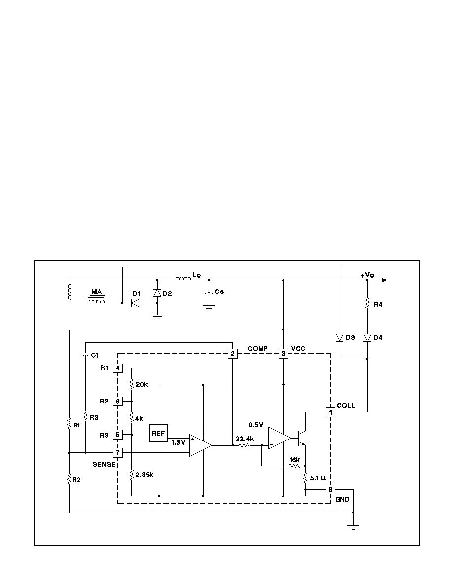
suffer the additional voltage drop of a series resistor.
Magnetic Amplifier Controller Application
The UC39431 makes an excellent controller for magnetic
amplifier regulated outputs. Working from either a square
wave drive or from a PWM signal controlled by another
output, a saturable reactor provides highly efficient con-
trol, requiring only a reset current which can be gener-
ated from its own output.
APPLICATION INFORMATION (cont.)
Figure 3. Magnetic amplifier controller application.
UDG-95090

6
UC19431
UC29431
UC39431
UC39431B
Figure 4. Internal 1.3V vs. temperature.
Figure 5. Error amp voltage gain and phase vs.
frequency.
UNITRODE CORPORATION
7 CONTINENTAL BLVD. ∑ MERRIMACK, NH 03054
TEL. (603) 424-2410 ∑ FAX (603) 424-3460
UDG-95092
UDG-95091
Table 1. Resistor divider connection table for shunt applications
REGULATED VOLTAGE
CONNECT R1 TO:
CONNECT R2 TO:
CONNECT R3 TO:
2.82V
SENSE (pin 7)
COLL (pin 1)
SENSE (pin 7)
3.12V
open
COLL (pin 1)
SENSE (pin 7)
5.1V
COLL (pin 1)
SENSE (pin 7)
open
7.8V
COLL (pin 1)
SENSE (pin 7)
GND (pin 8)
10.42V
COLL (pin 1)
SENSE (pin 7)
SENSE (pin 7)
12.24V
COLL (pin 1)
open
SENSE (pin 7)
Note: To obtain the shunt regulated or optocoupler sensed voltage specified in the left column, connect the internal resistors (R1,
R2, R3) as indicated. Refer to the shunt regulator application in Fig.1.

IMPORTANT NOTICE
Texas Instruments and its subsidiaries (TI) reserve the right to make changes to their products or to discontinue
any product or service without notice, and advise customers to obtain the latest version of relevant information
to verify, before placing orders, that information being relied on is current and complete. All products are sold
subject to the terms and conditions of sale supplied at the time of order acknowledgement, including those
pertaining to warranty, patent infringement, and limitation of liability.
TI warrants performance of its semiconductor products to the specifications applicable at the time of sale in
accordance with TI's standard warranty. Testing and other quality control techniques are utilized to the extent
TI deems necessary to support this warranty. Specific testing of all parameters of each device is not necessarily
performed, except those mandated by government requirements.
CERTAIN APPLICATIONS USING SEMICONDUCTOR PRODUCTS MAY INVOLVE POTENTIAL RISKS OF
DEATH, PERSONAL INJURY, OR SEVERE PROPERTY OR ENVIRONMENTAL DAMAGE ("CRITICAL
APPLICATIONS"). TI SEMICONDUCTOR PRODUCTS ARE NOT DESIGNED, AUTHORIZED, OR
WARRANTED TO BE SUITABLE FOR USE IN LIFE-SUPPORT DEVICES OR SYSTEMS OR OTHER
CRITICAL APPLICATIONS. INCLUSION OF TI PRODUCTS IN SUCH APPLICATIONS IS UNDERSTOOD TO
BE FULLY AT THE CUSTOMER'S RISK.
In order to minimize risks associated with the customer's applications, adequate design and operating
safeguards must be provided by the customer to minimize inherent or procedural hazards.
TI assumes no liability for applications assistance or customer product design. TI does not warrant or represent
that any license, either express or implied, is granted under any patent right, copyright, mask work right, or other
intellectual property right of TI covering or relating to any combination, machine, or process in which such
semiconductor products or services might be or are used. TI's publication of information regarding any third
party's products or services does not constitute TI's approval, warranty or endorsement thereof.
Copyright
©
1999, Texas Instruments Incorporated