 | –≠–ª–µ–∫—Ç—Ä–æ–Ω–Ω—ã–π –∫–æ–º–ø–æ–Ω–µ–Ω—Ç: UC3176QP | –°–∫–∞—á–∞—Ç—å:  PDF PDF  ZIP ZIP |

10/94
∑
Dual Power Operational Amplifiers
∑
±
2A Output Current Guaranteed
∑
Precision Current Sense Amplifier
∑
Two Supply Monitoring Inputs
∑
Parking Function and Under-Voltage
Lockout
∑
Safe Operating Area Protection
∑
3V to 35V Operation
Full Bridge Power Amplifier
UC3176
UC3177
FEATURES
DESCRIPTION
The UC3176/7 family of full bridge power amplifiers is rated for a continu-
ous output current of 2A. Intended for use in demanding servo applications
such as disk head positioning, the onboard current sense amplifier can be
used to obtain precision control of load current, or where voltage mode
drive is required, a standard voltage feedback scheme can be used. Out-
put stage protection includes foldback current limiting and thermal shut-
down, resulting in a very rugged device.
Auxiliary functions on this device include a dual input under-voltage com-
parator that can be programmed to respond to low voltage conditions on
two independent supplies. In response to an under-voltage condition the
power Op-Amps are inhibited and a high current, 100mA, open collector
drive output is activated. A separate Park/Inhibit command input.
The devices are operational over a 3V to 35V supply range. Internal un-
der-voltage lockout provides predictable power-up and power-down char-
acteristics.
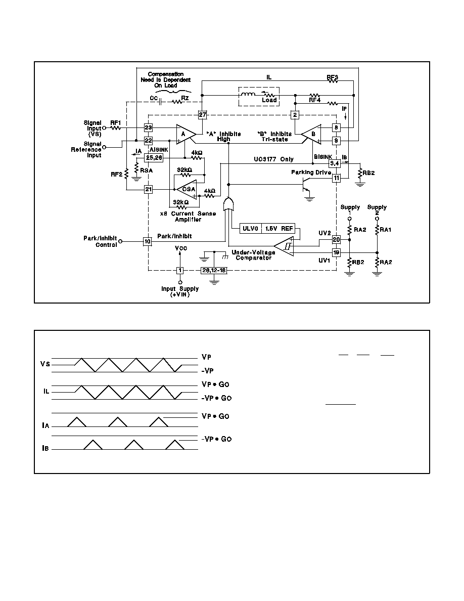
BLOCK DIAGRAM

Input Supply voltage, (+V
IN
) . . . . . . . . . . . . . . . . . . . . . . . 40V
Park/Inhibit, UV1 and UV2 inputs (zener clamped)
Maximum forced voltage . . . . . . . . . . . . . . . . -0.3V to 10V
Maximum forced current. . . . . . . . . . . . . . . . . . . . .
±
10mA
Other Input Voltages. . . . . . . . . . . . . . . . . . . . . -0.3V to +V
IN
Al
SINK
and Bl
SINK
Voltages . . . . . . . . . . . . . . . . . . -0.3V to 6V
Open Collector Output Voltages. . . . . . . . . . . . . . . . . . . . 40V
A and B Output Currents (Continuous)
Source . . . . . . . . . . . . . . . . . . . . . . . . . . Internally Limited
Sink. . . . . . . . . . . . . . . . . . . . . . . . . . . . . . . . . . . . . . . 2.5A
Total Supply Current (Continuous). . . . . . . . . . . . . . . . . . . 4A
Parking Drive Output Current (Continuous) . . . . . . . . 200mA
Supply OK Output Current, UC3177 (Continuous) . . . 30mA
Operating Junction Temperature . . . . . . . . -55∞C to +150∞C
Power Dissipation at TC = +75∞C
QP package. . . . . . . . . . . . . . . . . . . . . . . . . . . . . . . . . 4W
Storage Temperature . . . . . . . . . . . . . . . . . -65∞C to +150∞C
Note 1: Unless otherwise indicated, voltages are reference to
ground and currents are positive into, negative out of, the
specified terminals.
PARAMETER
TEST CONDITIONS
MIN.
TYP.
MAX. UNITS
Input Supply
Supply Current
+V
IN
= 12V
18
25
mA
+V
IN
= 35V
21
30
mA
UVOL Threshold
+V
IN
low to high
2.8
3.0
V
Threshold Hysteresis
220
300
mV
Power, Amplifier, A and B
Input Offset Voltage
V
CM
= 6V, V
OUT
= 6V
8
mV
Input Bias Current
V
CM
= 6V, Except A+ Input
-500
-100
nA
Input Bias Current at A+/Reference Input
(A+/Ref - BI
SINK
)/36kohms; T
J
= 25∞C
23
28
35
µ
A/V
Input Offset Current B Amp (UC3176 Only) V
CM
= 6V
200
nA
CMRR
V
CM
= 1 to 33V, +V
IN
=35V, V
OUT
= 6V
70
100
dB
PSRR
+V
IN
= 5 to 35V, V
CM
= 2.5V
70
100
dB
Large Signal Voltage Gain
V
OUT
= 3V, w/
IOUT
= 1A to V
OUT
= 9V, w/
IOUT
= -1A
1.5
4
V/mV
Thermal Feedback
+V
IN
= 20V, Pd = 20W at opposite output
25
200
µ
V/W
Saturation Voltage
I
OUT
= -2A, High Side, T
J
= 25∞
1.9
V
CI
OUT
= 2A, Low Side, T
J
= 25∞C
1.6
V
Total V
SAT
at 2A, T
J
= 25∞C
3.5
3.7
V
Unity Gain Bandwidth
1
MHz
Slew Rate
1
V/
µ
s
Differential I
OUT
Sense Error Current
I
OUT
(A) = -I
OUT
(B), /I
OUT
/- /AI
SINK
- BI
SINK/
in Bridge Configuration
I
OUT
200mA
3.0 6.0 mA
I
OUT
2A
5.0
10
mA
High Side Current Limiting
=V
IN
- V
OUT
< 12V
-2.7
-2.0
A
UC3176
UC3177
ABSOLUTE MAXIMUM RATINGS (Note 1)
QP package:
Thermal Resistance Junction to Leads,
JL
. . . . . . 15∞C/W
Thermal Resistance Junction to Ambient,
JA
. . . . 50∞C/W
THERMAL DATA
PACKAGE PIN FUNCTION
FUNCTION
PIN
+V
IN
1
B Output
2
BI
SINK
(Sense)
3
BI
SINK
4
N/C
5-7
B- Input
8
*
9
Park/Inhibit
10
Parking Drive
11
Gnd (Heat Flow Pins)
12-18
UV1
19
UV2
20
Current Feedback
21
A+ Input
22
A- Input
23
N/C
24
AI
SINK
25
AI
SINK
(Sense)
26
A Output
27
Gnd
28
*Pin 9: UC3176, B+ Input
UC3177, Supply OK
PLCC-28 (Top View)
QP Package
CONNECTION DIAGRAM
ELECTRICAL CHARACTERISTICS:
Unless otherwise stated, specifications hold for T
A
= 0 to 70∞C, +V
IN
= 12V, T
A
= T
J.
2
PARAMETER
TEST CONDITIONS
MIN.
TYP.
MAX. UNITS
Current Sense Amplifier
Input Offset Voltage
V
CM
= 0V, A+/Ref at 6V
3
mV
Ref = 2V to 20V, +V
IN
= 35, change with Ref
input voltage
600
µ
V/V
Thermal Gradient Sensitivity
+V
IN
= 20V, Ref = 10V Pd = 20W @ A or B
output
5.0
75
µ
V/W
PSRR
Ref = 2.5V, +V
IN
= 5 to 35V
70
100
dB
Gain
/AI
SINK
- BI
SINK
/
0.5V
7.8
8
8.1
V/V
Slew Rate
2
V/
µ
S
3dB Bandwidth
1
MHz
Max Output Current
I
SOURCE
= +V
IN
- V
OUT
= 0.5V
2.5
3.5
mA
Output Saturation Voltage
I
SOURCE
= 1.5mA, High Side
0.15
0.30
V
I
SINK
= 5mA, Low Side
1.4
1.7
V
Under-Voltage Comparator
Threshold Voltage
Low to High, other input at 5V
1.44
1.50
1.56
V
Threshold Hysteresis
50
70
80
mV
Input Current
Input = 2V, other input at 5V
-2
-.05
µ
A
Supply OK V
SAT
(UC3177 Only)
I
OUT
= 5mA
0.45
V
Supply OK Leakage (UC3177 Only)
V
OUT
= 35V
5
µ
A
Park/Inhibit
Park/Inhibit Thl'd
1.1
1.3
1.7
V
Park/Inhibit Input Current
At threshold
60
100
µ
A
Parking Drive Saturation Voltage
I
OUT
= 100mA
0.3
0.7
V
Parking Drive Leakage
V
OUT
= 35V
15
µ
A
Thermal Shutdown
Shutdown Temperature
165
∞C
UC3176
UC3177
ELECTRICAL CHARACTERISTICS:
Unless otherwise stated, specifications hold for T
A
= 0 to 70∞C, +V
IN
= 12V, T
A
= T
J.
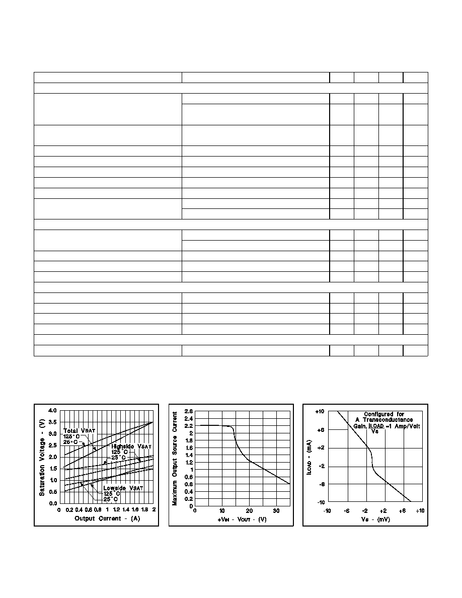
Output Saturation Voltage
vs Current
Maximum Source Current
vs +V
IN
- V
OUT
Crossover Current Error
Characteristic
3
UC3176
UC3177
Transconductance (G
O
) =
I
L
V
S
=
R
F2
R
F1
◊
1
8
R
S
with: R
SA
= R
SB
and R
F3
= R
F4
Parking Current (I
P
) =
V
IN
-
1.5
R
P
+
R
L
where: R
L
= load resistance
Under-Voltage Thresholds, at Supplies
High to Low Threshold, (V
LH
) = 1.425 (R
A
+ R
B
)/R
B
Low to High Threshold, (V
HL
) = 1.5 (R
A
+ R
B
)/R
B
APPLICATION AND OPERATION INFORMATION
DESIGN EQUATIONS
WAVEFORMS FOR ABOVE APPLICATION
UNITRODE INTEGRATED CIRCUITS
7 CONTINENTAL BLVD.
∑
MERRIMACK, NH 03054
TEL. (603) 424-2410
∑
FAX (603) 424-3460
4

IMPORTANT NOTICE
Texas Instruments and its subsidiaries (TI) reserve the right to make changes to their products or to discontinue
any product or service without notice, and advise customers to obtain the latest version of relevant information
to verify, before placing orders, that information being relied on is current and complete. All products are sold
subject to the terms and conditions of sale supplied at the time of order acknowledgement, including those
pertaining to warranty, patent infringement, and limitation of liability.
TI warrants performance of its semiconductor products to the specifications applicable at the time of sale in
accordance with TI's standard warranty. Testing and other quality control techniques are utilized to the extent
TI deems necessary to support this warranty. Specific testing of all parameters of each device is not necessarily
performed, except those mandated by government requirements.
CERTAIN APPLICATIONS USING SEMICONDUCTOR PRODUCTS MAY INVOLVE POTENTIAL RISKS OF
DEATH, PERSONAL INJURY, OR SEVERE PROPERTY OR ENVIRONMENTAL DAMAGE ("CRITICAL
APPLICATIONS"). TI SEMICONDUCTOR PRODUCTS ARE NOT DESIGNED, AUTHORIZED, OR
WARRANTED TO BE SUITABLE FOR USE IN LIFE-SUPPORT DEVICES OR SYSTEMS OR OTHER
CRITICAL APPLICATIONS. INCLUSION OF TI PRODUCTS IN SUCH APPLICATIONS IS UNDERSTOOD TO
BE FULLY AT THE CUSTOMER'S RISK.
In order to minimize risks associated with the customer's applications, adequate design and operating
safeguards must be provided by the customer to minimize inherent or procedural hazards.
TI assumes no liability for applications assistance or customer product design. TI does not warrant or represent
that any license, either express or implied, is granted under any patent right, copyright, mask work right, or other
intellectual property right of TI covering or relating to any combination, machine, or process in which such
semiconductor products or services might be or are used. TI's publication of information regarding any third
party's products or services does not constitute TI's approval, warranty or endorsement thereof.
Copyright
©
1999, Texas Instruments Incorporated