 | –≠–ª–µ–∫—Ç—Ä–æ–Ω–Ω—ã–π –∫–æ–º–ø–æ–Ω–µ–Ω—Ç: UC3178QP | –°–∫–∞—á–∞—Ç—å:  PDF PDF  ZIP ZIP |
5/93
UC3178
Full Bridge Power Amplifier
∑
Precision Current Control
∑
±
450mA Load Current
∑
1.2V Typical Total Vsat at
450mA
∑
Programmable Over-Current
Control
∑
Range Control for 4:1 Gain
Change
∑
Compensation Adjust Pin for
Range Bandwidth Control
∑
Inhibit Input and UVLO
∑
3V to 15V Operation
∑
12mA Quiescent Supply
Current
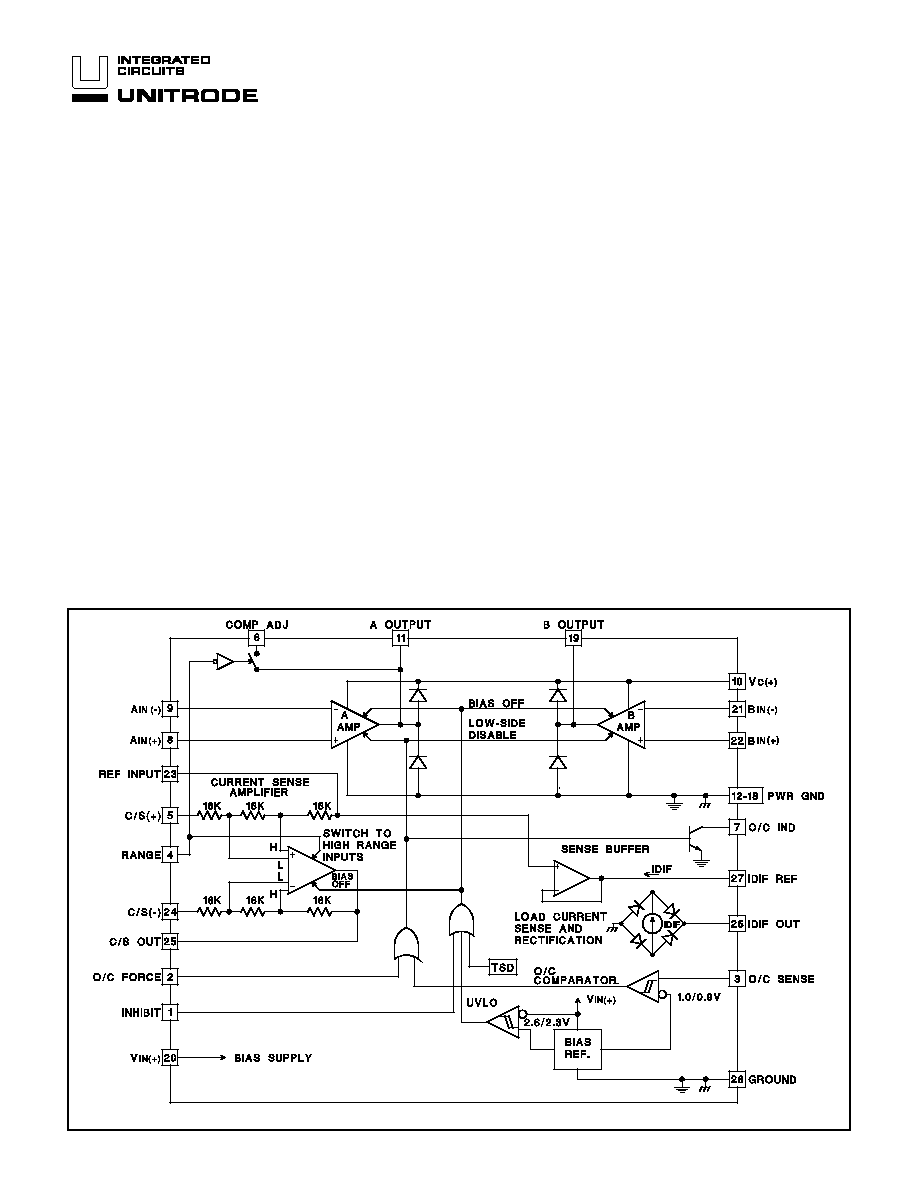
The UC3178 full-bridge power amplifier, rated for continuous output current
of 0.45 Amperes, is intended for use in demanding servo applications. This
device includes a precision current sense amplifier that senses load current
with a single resistor in series with the load. The UC3178 is optimized to con-
sume a minimum of supply current, and is designed to operate in both 5V
and 12V systems. The power output stages have a low saturation voltage
and are protected with current limiting and thermal shutdown. When inhibited,
the device will draw less than 1.5mA of total supply current.
Auxiliary functions on this device include a load current sensing and rectifica-
tion function that can be configured with the device's over-current comparator
to provide tight control on the maximum commanded load current. The closed
loop transconductance of the configured power amplifier can be switched be-
tween a high and low range with a single logic input. The 4:1 change in gain
can be used to extend the dynamic range of the servo loop. Bandwidth vari-
ations that would otherwise result with the gain change can be controlled with
a compensation adjust pin.
This device is packaged a power PLCC, "QP" package which maintains a
standard 28-pin outline, but with 7 pins along one edge directly tied to the die
substrate for improved thermal performance.
FEATURES
BLOCK DIAGRAM
DESCRIPTION
UDG-92010
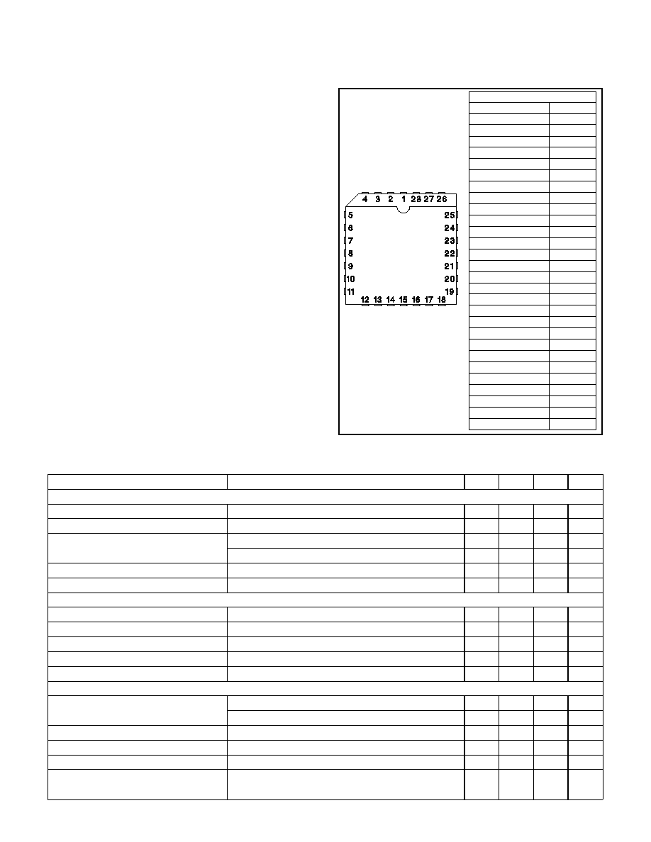
PLCC - 28 (Top View)
QP Package
ABSOLUTE MAXIMUM RATINGS
THERMAL DATA
UC3178
Input Supply Voltage, (V
IN
(+), V
C
(+)) . . . . . . . . . . . . . . . . . . 20V
O/C Sense, Logic Inputs, and REF Input
Maximum forced voltage . . . . . . . . . . . . . . . . . -0.3V to 10V
Maximum forced current . . . . . . . . . . . . . . . . . . . . . .
±
10mA
A & B Amplifier Inputs . . . . . . . . . . . . . -0.3V to (V
IN
(+) + 1.0V)
O/C Indicate Open Collector Output Voltage . . . . . . . . . . . . 20V
A and B Output Currents(continuous)
Source . . . . . . . . . . . . . . . . . . . . . . . . . . . . Internally Limited
Sink . . . . . . . . . . . . . . . . . . . . . . . . . . . . . . . . . . . . . . . . 0.6A
Output Diode Current (pulsed)* . . . . . . . . . . . . . . . . . . . . . 0.5A
O/C Ind Output Current(continuous) . . . . . . . . . . . . . . . . 20mA
Operating Junction Temperature . . . . . . . . . . . . . . . . . . +150
∞
C
Storage Temperature . . . . . . . . . . . . . . . . . . . -65
∞
C to +150
∞
C
*Notes: Unless otherwise indicated, voltages are referenced to
ground and currents are positive into, negative out of, the speci-
fied terminals, "Pulsed" is defined as a less than 10% duty cy-
cle pulse with a maximum duration of 500
µ
s
.
QP package: (see packaging section of UICC data book for more
details on thermal performance)
Thermal Resistance Junction to Leads,
jl . . . . . . . . 15
∞
C/W
Thermal Resistance Junction to Ambient,
ja . . . 30-40
∞
C/W
CONNECTION DIAGRAM
PARAMETER
TEST CONDITIONS
MIN
TYP
MAX
UNITS
Input Supply
V
IN
(+)Supply Current
12
16
mA
V
C
(+) Supply Current
I
OUT
= OA
1.2
2.0
mA
Total Supply Current
Supplies = 5V,I
OUT
= OA
12
16
mA
Supplies = 12V,I
OUT
= OA
13
18
mA
V
IN
(+) UVLO Threshold
low to high
2.6
2.8
V
UVLO Threshold Hysterisis
300
mV
Over-Current (O/C) Comparator
Input Bias Current
V input = 0.8V
-1.0
-.01
µ
A
Thresholds
low to high
0.97
1.0
1.03
V
Threshold Hysterisis
85
100
115
mV
O/C IND Vsat
I
OUT
= 5mA, V input low
0.2
0.45
V
O/C IND Leakage
V
OUT
= 20V
5.0
µ
A
Power Amplifiers A and B
Input Offset Voltage
A Amplifier, V
CM
= 6V
4.0
mV
B Amplifier, V
CM
= 6V
12.0
mV
Input Bias Current
V
CM
= 6V
-500
-50
µ
CMRR
V
CM
= 0.5 to 13V, Supplies = 15V
70
90
dB
PSRR
V
IN
(+) = 4 to 15V, V
CM
= 1.5V
70
90
dB
Large Signal Voltage Gain
Supplies = 12V, V
OUT
= 1V, I
OUT
= 300mA
to V
OUT
= 10.5V, I
OUT
= -300mA
3.0
15.0
V/mV
Unless otherwise stated specifications hold for T
A
= 0
∞
C to 70
∞
C, V
C
(+) = V
IN
(+) =
12V, REF Input = V
IN
(+)/2, O/C Input & Inhibit Input = 0V.
Note: The above numbers for
jl are maximums for the limiting
thermal resistance of the package in a standard mounting con-
figuration. The
ja numbers are meant to be guidelines for the
thermal performance of the device/pc-board system. All of the
above numbers assume no ambient airflow.
PACKAGE PIN FUNCTION
FUNCTION
PIN
Inhibit
1
O/C Force
2
O/C Sense
3
Range
4
C/S(+)
5
Comp Adj
6
O/C Ind
7
A
IN
(+) 8
A
IN
(-)
9
V
C
(+) Supply
10
A Output
11
Pwr Gnd
12
Pwr Gnd
13
Pwr Gnd
14
Pwr Gnd
15
Pwr Gnd
16
Pwr Gnd
17
Pwr Gnd
18
B Output
19
V
IN
(+) 20
B
IN
(-)
21
B
IN
(+) 22
REF Input
23
C/S(+)
24
C/S Out
25
IDIF Out
26
IDIF REF
27
Ground
28
ELECTRICAL CHARACTERISTICS:
2
PARAMETER
TEST CONDITIONS
MIN
TYP
MAX
UNITS
Power Amplifiers A & B (cont.)
Gain Bandwith Product
A Amplifier
2.0
MHz
B Amplifier
1.0
MHz
Slew Rate
1.0
V/
µ
s
High-Side Current Limit
0.45
0.65
A
Output Saturation Voltage
High-Side, I
OUT
= -100mA
0.75
V
High-Side, I
OUT
= -300mA
0.85
V
High-Side, I
OUT
= -450mA
0.9
V
Low-Side, I
OUT
= 100mA
0.2
V
Low-Side, I
OUT
= 300mA
0.25
V
Low-Side, I
OUT
= 450mA
0.30
V
Total Vsat, I
OUT
= 100mA
0.95
1.2
V
Total Vsat, I
OUT
= 300mA
1.05
1.4
V
Total Vsat, I
OUT
= 450mA
1.25
1.6
V
High-Side Diode, Vf
I
D
= 450mA
1.30
V
Current Sense Amplifier
Input Offset Voltage
V
CM
= 6V, Low range mode
2.0
mV
High range mode
4.0
mV
Input Offset Change
V
CM
= -1V to 13V, Supplies = 12V, Low Range Mode
2000
µ
V/V
with Common Mode Input
V
CM
= -1V to 13V, Supplies = 12V, High Range Mode
4000
µ
V/V
Voltage Gain
V
DIFF
= +1.0 to -1.0V, Vcm = 6V, High Range Mode
0.485
0.50
0.515
V/V
V
DIFF
= +1.0 to -1.0V, Vcm = 6V, Low Range Mode
1.95
2.0
2.05
V/V
Saturation Voltage
Low-Side, I
OUT
= 1mA
0.1
0.3
V
High-Side, I
OUT
= -1mA, Referenced to = V
IN
(+)
0.1
0.3
V
Input Bias Current at Ref. Input
(REF Input - C/S(+))/48kohms, Tj = 25
∞
C
15
21
27
µ
A/V
Load Current Sense and Rectification
Sense Buffer Offset Voltage
REF Input to IDIF REF, I
OUT
=
±
1mA 10
mV
Sense Buffer CMRR
I
OUT
=
±
1mA, REF Input = 2V to 10V
70
90 dB
IDIF REF to IDIF Out Current
IDIF =
±
100
µ
A, IDIF Out = 1V
0.95
1.0
1.05
A/A
Ratio
IDIF =
±
1mA, IDIF Out = 1V
0.94
1.0
1.06
A/A
IDIF Out Supply Sensitivity
IDIF Out =
±
1mA, V
IN
(+) = 4V to 15V,REF Input = 2V
1.0
5.0
µ
A/V
IDIF Out Common Mode Sensitivity
I
OUT
=
±
1mA, REF Input = 2V to10V, IDIF Out = 1V
(delta IDIF Out/delta REF Input)
1.0
5.0
µ
A/V
Auxiliary Functions
Inhibit Input Threshold
0.6
1.1
1.7
V
Inhibit Input Current
Inhibit Input = 1.7V
-1.0
-0.5
µ
A
O/C Force Input Threshold
0.6
1.1
1.7
V
O/C Force Input Current
O/C Force Input = 1.7V
50
100
µ
A
Range Input Threshold
0.6
1.1
1.7
V
Range Input Current
Range Input = 1.7V
50
100
µ
A
COMP ADJ Pin Saturation
Range Input = 0V, Pin Current =
±
500
µ
A, Referenced
Voltage
to A
OUT
0.02
0.1
V
COMP ADJ Leakage Current
Range Input = 1.7V, Supplies = 12V
A
OUT
-V
Comp Adj
=
±
6V
5.0
µ
A
Total Supply Current When Inhibited
V
IN
(+) and V
C
(+) currents
1.0
1.5
mA
Thermal Shutdown Temperature
165
∞
C
UC3178
Unless otherwise stated specifications hold for T
A
= 0
∞
C to 70
∞
C , V
C
(+) = V
IN
(+) = 12V,
REF Input = V
IN
(+)/2, O/C Input & Inhibit Input = 0V.
ELECTRICAL
CHARACTERISTICS (cont.):
3

A & B OUT: Outputs for the A & B power amplifiers,
providing differential drive to the load during normal op-
eration. During a UVLO, Inhibit, or O/C condition both of
these outputs will be in a high, source only state. High-
side diodes are included to catch inductive load currents
flowing into these pins, inductive kicks on the low-side are
caught by the high-side output transistors.
A
IN
(+): Non-inverting input to the A amplifier. Normally tied
to the REF Input when the current sense amplifier is used.
A
IN
(-): Inverting input to the A amplifier. Used as the sum-
ming node to close the loop on the overall power
amplifier.
B
IN
(+):
Non-inverting input to the B amplifier. This pin nor-
mally sets the reference point for the differential voltage
swing at the load.
B
IN
(-): Inverting input to the B amplifier. Used to program
the gain of the B amplifier.
COMP ADJ: The compensation adjust pin allows the user
to provide an auxiliary compensation network for the A am-
plifier that is only active when the current sense amplifier is
in the low range. With this option, the user can control the
change in bandwidth that would otherwise result from the
gain change in the feedback loop.
C/S(+): The non-inverting input to the current sense ampli-
fier is typically tied to the load side of the series current
sense resistor. This pin can be pulled below ground during
an abrupt load current change with an inductive load.
Proper operation of the current sense amplifier will result if
this pin does not go below ground by an amount greater
than:
(REF Input / 2 ) - 0.3V.
C/S(-): The inverting input to the current sense amplifier is
typically tied to the connection between the B amplifier
output and the current sense resistor that is in series with
the load.
C/S Output: The output of the current sense amplifier has
a 1.5mA current source pull-up and an active NPN pull-
down. The output will pull to within 0.3V of either rail with
a load current of less than 1mA.
GND: Reference point for the internal reference, O/C
comparator, and other low-level circuitry.
IDIF OUT: Current source output pin. The value of the out-
put current is nominally equal to the magnitude of the
current through the IDIF REF pin.
IDIF REF: Output of the IDIF sense buffer. Voltage on this
pin will track the applied voltage on the REF Input pin.
Current through this pin is full wave rectified and appears
as a current sourced from the IDIF OUT pin.
Inhibit : A high impedance logic input that disables the A
and B power amplifiers, the IDIF sense buffer, and the
Current Sense amplifier. This input has an internal pull-up
that will inhibit the device if the input is left open.
O/C Force: Logic input that forces the O/C condition.
O/C IND: Open collector ouput that indicates, with an ac-
tive low state, an O/C condition.
O/C Sense: Input to the Over Current Comparator. When
this input is above its 1V threshold the low-side devices of
both the A & B power amplifiers will be disabled forcing a
high, source only, state at both outputs.
PWR GND: Current return for all high level circuitry, this
pin should be connected to the same potential as GND.
Range: When this pin is open or at a logic low potential,
the current sense amplifier will be in its low range mode.
In this mode the voltage gain of the amplifier will be 2. If
this pin is brought to a logic high, the gain of the current
sense amplifier will change into its high range value of
0.5. This factor of four change in gain will vary the overall
transconductance of the power amplifier by the same ra-
tio, with the transconductance being the highest in the
high mode. This feature allows improved dynamic range
of load current control for a given control input range and
resolution.
REF Input: Sets the Reference level at the C/S Output,
and is normally tied to the system reference level for in-
puts to the power amplifier.
V
IN
(+): Provides bias supply to the device. The High-Side
drive to the power stages on both the A and B amplifiers
is referenced to this pin. The High-side saturation volt-
ages, and UVLO are specified and measured with respect
to this supply pin.
V
C
(+): This supply pin is the high current supply to the
collectors of the high-side NPN output devices on the A
and B amplifiers. This supply should be powered when-
ever the A or B amplifiers are to be activated. This pin can
operate approximately 400mV below the V
IN
(+) supply
without affecting the voltage available to the load.
UC3178
PIN DESCRIPTIONS:
4
UC3178
UNITRODE INTEGRATED CIRCUITS
7 CONTINENTAL BLVD.
∑
MERRIMACK, NH 03054
TEL (603) 424-2410
∑
FAX (603) 424-3460
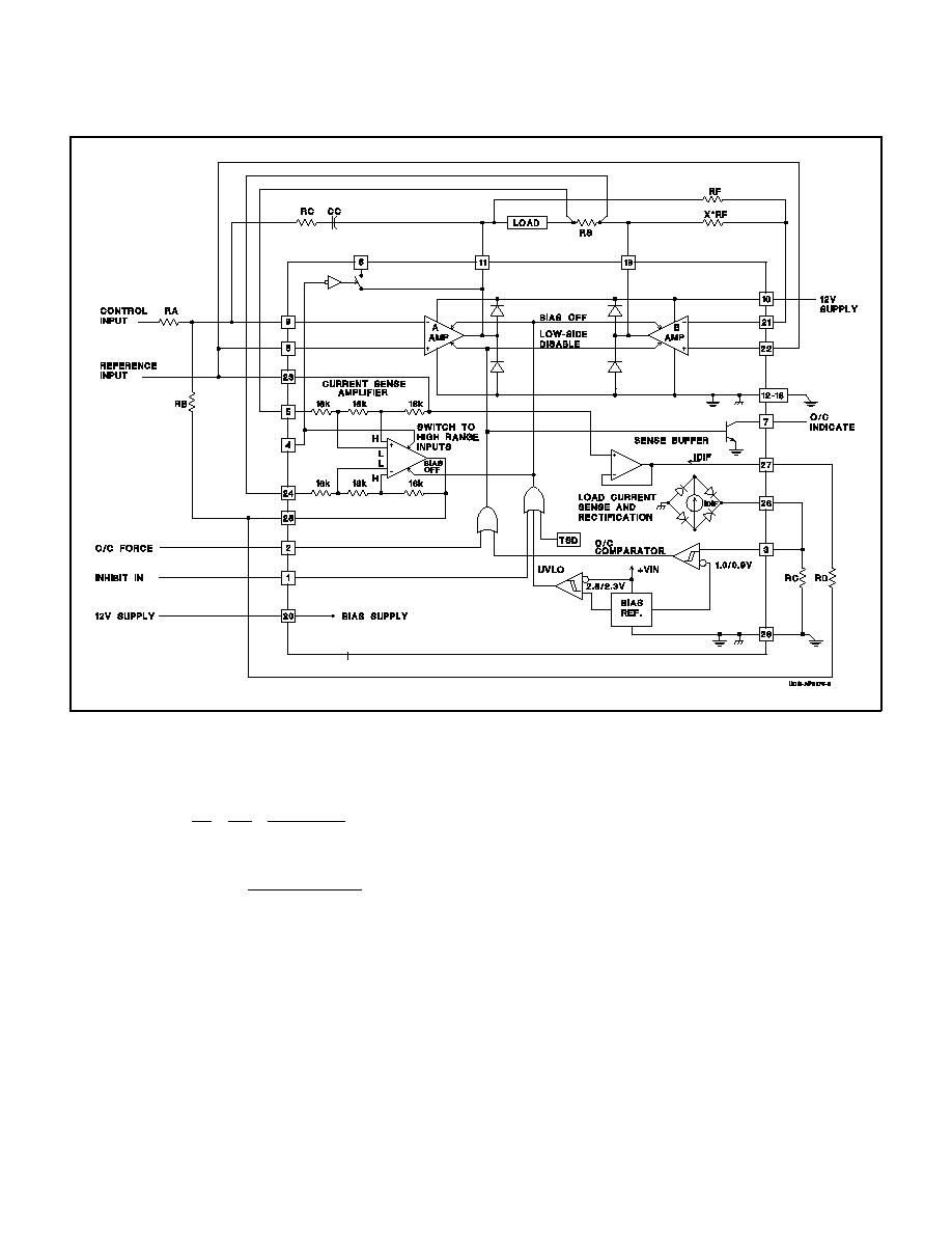
TYPICAL APPLICATION
Power amplifier transconductance
Go
=
Il
Vs
=
RB
RA
∑
1
AV
CS
∑
RS
Peak commanded load current
Il
MAX
=
V
o/c
∑
RD
RS
∑
AV
CS
∑
RE
where:
Il is the load current
Vs is the input command voltage
AV
CS
is the current sense amplifier gain
= 2.0 in low range mode
= 0.5 in high range mode
V
O/C
is the 1.0V over-current comparator threshold
UDG-92009
5

IMPORTANT NOTICE
Texas Instruments and its subsidiaries (TI) reserve the right to make changes to their products or to discontinue
any product or service without notice, and advise customers to obtain the latest version of relevant information
to verify, before placing orders, that information being relied on is current and complete. All products are sold
subject to the terms and conditions of sale supplied at the time of order acknowledgement, including those
pertaining to warranty, patent infringement, and limitation of liability.
TI warrants performance of its semiconductor products to the specifications applicable at the time of sale in
accordance with TI's standard warranty. Testing and other quality control techniques are utilized to the extent
TI deems necessary to support this warranty. Specific testing of all parameters of each device is not necessarily
performed, except those mandated by government requirements.
CERTAIN APPLICATIONS USING SEMICONDUCTOR PRODUCTS MAY INVOLVE POTENTIAL RISKS OF
DEATH, PERSONAL INJURY, OR SEVERE PROPERTY OR ENVIRONMENTAL DAMAGE ("CRITICAL
APPLICATIONS"). TI SEMICONDUCTOR PRODUCTS ARE NOT DESIGNED, AUTHORIZED, OR
WARRANTED TO BE SUITABLE FOR USE IN LIFE-SUPPORT DEVICES OR SYSTEMS OR OTHER
CRITICAL APPLICATIONS. INCLUSION OF TI PRODUCTS IN SUCH APPLICATIONS IS UNDERSTOOD TO
BE FULLY AT THE CUSTOMER'S RISK.
In order to minimize risks associated with the customer's applications, adequate design and operating
safeguards must be provided by the customer to minimize inherent or procedural hazards.
TI assumes no liability for applications assistance or customer product design. TI does not warrant or represent
that any license, either express or implied, is granted under any patent right, copyright, mask work right, or other
intellectual property right of TI covering or relating to any combination, machine, or process in which such
semiconductor products or services might be or are used. TI's publication of information regarding any third
party's products or services does not constitute TI's approval, warranty or endorsement thereof.
Copyright
©
1999, Texas Instruments Incorporated