 | –≠–ª–µ–∫—Ç—Ä–æ–Ω–Ω—ã–π –∫–æ–º–ø–æ–Ω–µ–Ω—Ç: UC3584N | –°–∫–∞—á–∞—Ç—å:  PDF PDF  ZIP ZIP |
UC1584
UC2584
UC3584
03/99
FEATURES
∑
Practical Operation at Switching
Frequencies up to 1MHz
∑
Wide Band Error Amplifier
∑
Undervoltage Lockout with Hysteresis
∑
Output Active Low During UVLO
∑
Soft Start/Maximum Duty Cycle
Control
∑
Trimmed Bandgap Reference
∑
Internally Regulated 15V Boost
Supply
∑
Short Circuit Protection with
Programmable Delay
Secondary Side Synchronous Post Regulator
DESCRIPTION
The UC3584 is a low voltage, Secondary Side Synchronous Post Regula-
tor. It is intended to be used for auxiliary output voltage regulation in single
secondary winding, multiple output power supplies (for more details refer
to the Application Section of this Data sheet). The UC3584 is most suited
for systems where the main output is regulated between 5V and 14V. Out-
put voltages regulated by the UC3584 can range from virtually 0V up to
the output voltage of the main output.
Auxiliary output voltage regulation with the UC3584 uses leading edge
modulation making it compatible to primary side peak current or voltage
mode control. The UC3584 clock circuit is synchronized to the switching
frequency utilizing the falling edge of the transformer's secondary winding
waveform.
15
13
14
16
11
9
10
12
SYNC
CT
RT
VREG
VCC
220pF
15k
100pF
1k
BST2
PGND
FB
BST1
0.1
µ
F
1N4148
0.1
µ
F
10
µ
F
SOLID
TANTALUM
+
1N4148
33
µ
H
COLTRONICS
470
µ
F
+
2
4
3
1
6
8
7
5
COMP
SS
CDLY
GND
SRC
OUT
VFLT
1.5
µ
F
120pF
1000pF
0.1
µ
F
3300pF
20k
30.1k
1500pF
1.33k
24.3k
3.3V
AUX
100
1.5W
0.1
µ
F
390
µ
F
33
µ
H
COILTRONICS
CSHD
10-45L
IRFR024
4.75k
3.57k
3.3
+
+
+
+
7
µ
H
OS-CON
330
µ
F
+
1
µ
F
+
5V
MAIN
170kHz
PUSH-PULL
2
2
10
10
10BQ040
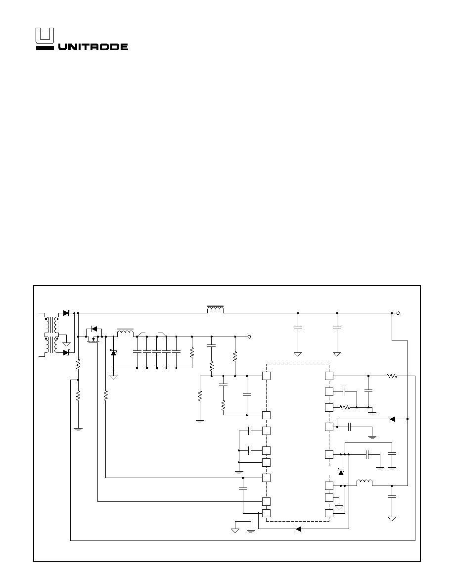
TYPICAL APPLICATION DIAGRAM.
UDG-99062
2
UC1584
UC2584
UC3584
ABSOLUTE MAXIMUM RATINGS
Supply Voltage . . . . . . . . . . . . . . . . . . . . . . . . . . . . . . . . . . 20V
V
FLT
Voltage . . . . . . . . . . . . . . . . . . . . . . . . . . . 50V, 30V at 2A
Supply Current . . . . . . . . . . . . . . . . . . . . . . . . . . . . . . . . . 50mA
Analog Inputs. . . . . . . . . . . . . . . . . . . . . . . . . . . . . . ≠0.3 to 20V
SYNC Maximum Sink Current . . . . . . . . . . . . . . . . . . . . . 600
µ
A
PWM Driver, I
OUT
. . . . . . . . . . . . . . . . . . . . . . . . . . . .
±
300mA
PWM Driver, I
OUT
(Peak) . . . . . . . . . . . . . . . . . . . . . . . . .
±
1.5A
Maximum Operating Frequency . . . . . . . . . . . . . . . . . . . . 1MHz
Power Dissipation at T
A
= 60∞C . . . . . . . . . . . . . . . . . . . . . . 1W
Storage Temperature . . . . . . . . . . . . . . . . . . . . ≠65∞C to 150∞C
Junction Temperature . . . . . . . . . . . . . . . . . . . . ≠55∞C to 150∞C
Lead Temperature (Soldering, 10 sec.) . . . . . . . . . . . . . . 300∞C
Currents are positive into, negative out of specified terminal.
Consult Packaging Section of Databook for thermal limitations
and considerations of packages.
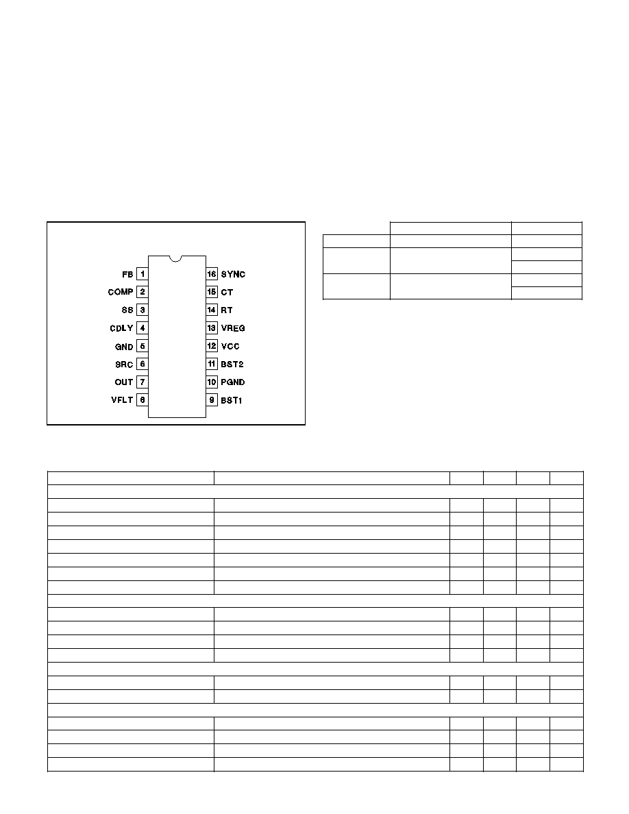
CONNECTION DIAGRAMS
DIL-16, SOIC-16 (Top View)
J, N or DW Packages
ELECTRICAL CHARACTERISTICS:
Unless otherwise specified, T
A
= 0∞C to 70∞C for the UC3584, ≠40∞C to 85∞C for
the UC2584, and ≠55∞C to 125∞C for the UC1584, VCC = 15V. T
A
= T
J
.
PARAMETERS
TEST CONDITIONS
MIN
TYPE
MAX
UNITS
Error Amplifier
FB
COMP = FB
1.468
1.5
1.532
V
I
FB
V
COMP
= V
FB
150
300
450
nA
COMP V
OL
FB = 1.6V, I
COMP
= 200
µ
A
50
400
mV
COMP V
OH
FB = 1.4V, I
COMP
= ≠200
µ
A
5.1
5.5
7
V
AVOL
60
80
dB
PSRR (COMP)
COMP = FB, VCC = 14V to 16V
60
dB
GBW Product
F = 100kHz
5
10
MHz
Oscillator
Frequency
R
T
= 3.75k, C
T
= 400pF, No Synchronization
500
kHz
Ramp Low
R
T
= 3.75k, C
T
= 400pF, No Synchronization
1.75
V
Ramp High
R
T
= 3.75k, C
T
= 400pF, No Synchronization
3.5
V
Ramp Amplitude
R
T
= 3.75k, C
T
= 400pF, No Synchronization
1.75
V
PWM
Maximum Duty Cycle
COMP = 4.5V
90
%
Minimum Duty Cycle
COMP = 0V
0
%
PWM DRIVER
V
SAT
High
V
FLT
≠ V
OUT
, I
OUT
= ≠100mA
2.5
3
V
V
SAT
Low
V
OUT
≠ V
SRC
, I
OUT
= 50mA
0.8
2.2
V
T
RISE
Load = 1nF, SRC = 0V, Measure V
OUT
1V to 9V
75
100
ns
T
FALL
Load = 1nF, SRC = 0V, Measure V
OUT
9V to 1V
25
100
ns
TEMPERATURE RANGE
PACKAGE
UC1584J
≠55∞C to +125∞C
CDIP
UC2584DW
≠40∞C to +85∞C
SOIC-Wide
UC2584N
PDIP
UC3584DW
0∞C to +70∞C
SOIC-Wide
UC3584N
PDIP
ORDERING INFORMATION

3
UC1584
UC2584
UC3584
ELECTRICAL CHARACTERISTICS:
Unless otherwise specified, T
A
= 0∞C to 70∞C for the UC3584, ≠40∞C to 85∞C for the
UC2584, and ≠55∞C to 125∞C for the UC1584, VCC = 15V. T
A
= T
J
.
PARAMETERS
TEST CONDITIONS
MIN
TYPE
MAX
UNITS
Soft Start
Charge Current
30
µ
A
Discharge Current
1
mA
SS Delay
C
SS
= 500nF
50
ms
Fault Latch
Charge Current
30
µ
A
Discharge Current
5
mA
Fault Latch Delay
CDLY = 500nF
50
ms
UVLO
VCC On
10.5
V
Hysteresis
1.7
V
Regulated Voltage
V
REG
I
REG
= 0mA to 1mA
4.8
5.2
V
VCC Regulator
VCC
Boost inductor connected to 5V
14
15
16
V
I
CC
No Load, Boost Circuitry Inactive
12
40
mA
No Load, Boost Circuitry Active (Note 1)
55
mA
Note 1: Guaranteed by design. Not 100% tested in production.
BLOCK DIAGRAM
UDG-97141

4
UC1584
UC2584
UC3584
PIN DESCRIPTIONS
BST1: Collector of the boost switch. This is the
connection point of the external boost inductor and boost
diode. The boost converter generates the bias supply for
the UC3584 from the regulated 5V output.
BST2: See BST1. BST2 must be connected externally
to BST1 pin.
CDLY: Delay Set.
External CDLY capacitor sets the
delay from the time Short Circuit condition is detected
and Fault Condition is asserted.
COMP: Output of the Voltage Error Amplifier.
CT: Connect the Timing Capacitor between CT and GND.
FB: Inverting Input of the Voltage Error Amplifier.
GND: Analog System Ground.
OUT: Output of the floating driver for an external,
N-channel MOSFET.
PGND: Power Ground. This is the reference node for the
boost bias supply regulator. PGND and GND must be
connected externally.
RT: A Timing Resistor connected between RT and GND
sets the discharge current of the timing capacitor.
SRC: Source connection of the floating driver to the
external switch.
SS: Soft Start. An external capacitor is connected
between SS and GND to set the duration of the Soft
Start cycle.
SYNC:
Synchronization
Pin.
The
UC3584
is
synchronized from the falling edge of the transformer's
secondary winding. Voltage must exceed 1V at minimum
input line.
VCC: Bias supply of the chip, approximately 15V. This is
also the output of the boost regulator. The VCC pin must
be decoupled to PGND.
VFLT: Positive rail of the floating driver's bias supply.
Decouple to SRC using a high frequency (ceramic)
capacitor.
VREG: Output of the internal 5V regulated supply. Must
be decoupled to GND.
Biasing the UC3584
Bias supply for the UC3584 is generated from the main
output of the power supply by a boost regulator. The in-
ductor, diode and capacitor of the boost converter are ex-
ternal components, while the boost switch is internal to
the chip. The boost converter operates in a burst mode
with a built-in hysteresis of approximately 1V centered at
15V. This is a bang-bang controller and when enabled
has a fixed duty cycle of 75%.
Undervoltage Detection
The UVLO circuit of the UC3584 monitors the voltage on
VCC. During power up and power down, the pulse width
modulator and the output driver are disabled and OUT is
held active low. Operation is enabled when VCC reaches
10.5V. The UVLO circuitry has a built-in hysteresis of
1.7V (10.5V to 8.8V) thus VCC must drop below 8.8V in
order to assert UVLO again.
Precision Reference
An internal precision bandgap reference provides accu-
rate voltages to the error amplifier and other control sec-
tions of the IC. A buffered 5V regulated voltage is also
available for external circuitry on the VREG pin. This pin
must be decoupled to the signal GND connection by a
good quality high frequency capacitor.
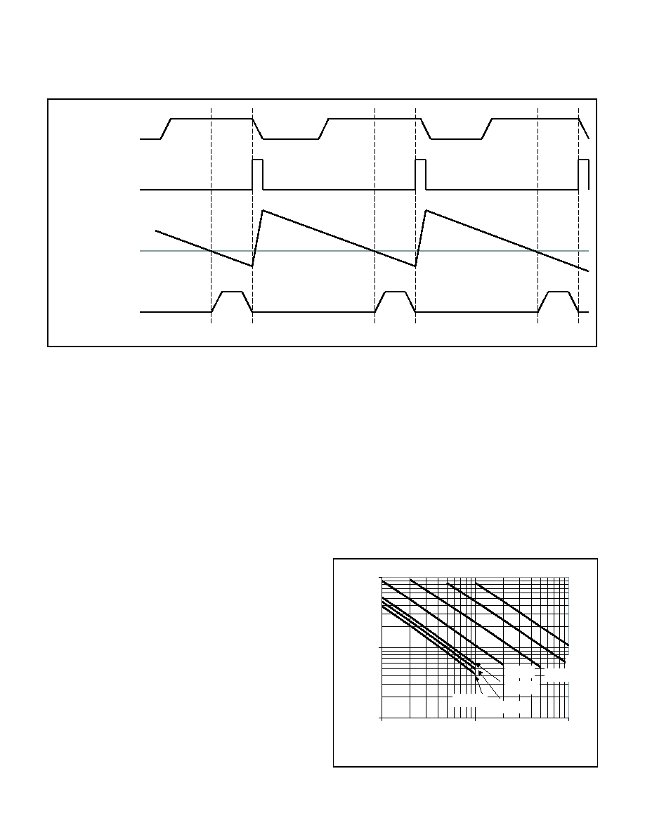
Oscillator and Trailing Edge Synchronization
The UC3584 is outfitted with a synchronizable oscillator
which also generates a ramp signal across the C
T
capac-
itor for the PWM comparator. For easy implementation of
the leading edge pulse width modulation technique, the
oscillator has an inverted ramp waveform as shown in
Fig. 1. The free running oscillator frequency is deter-
mined by the timing components, R
T
and C
T
, according
to the following approximate equations:
R
D
T
MAX
=
-
9 3
1
1 7
.
.
(
)
(
)
f
C
R
C
OSC
T
T
T
=
-
◊
∑
∑
2
8 2 10
8
0 9
.
.
where
R
T
is the timing resistor, its value should be between
1k
and 100k
,
C
T
is the timing capacitor,
D
MAX
is the desired maximum duty cycle, and
f
OSC
is the free running oscillator frequency.
Figure 2 graphically depicts the measured frequency
data.
APPLICATION INFORMATION
5
UC1584
UC2584
UC3584
Edge Modulation
During normal operation the oscillator must be synchro-
nized to the falling edge of the transformer secondary
waveform. Synchronization is achieved by connecting
SYNC to the secondary winding via a resistor divider.
The resistor divider must be chosen to provide a SYNC
pin voltage in excess of 1V at the lowest operating volt-
age on the transformer secondary winding. The UC3584
will generate a narrow internal synchronization pulse
which will synchronize the oscillator to the switching fre-
quency of the main converter.
PWM and Output Driver
The UC3584 employs leading edge modulation tech-
nique to set the required on time of its output. Leading
edge modulation is preferred for secondary side regula-
tion in multiple output converters to prevent ambiguity in
the primary current waveform. In fact, this is the only fea-
sible technique to preserve compatibility with primary
side peak current mode control.
As Fig. 1 depicts the UC3584 utilizes voltage mode con-
trol to regulate output voltage. The output pulse width
(the on-time of the MOSFET switch) is determined on a
cycle-by-cycle basis by comparing the output of the volt-
age error amplifier and the ramp waveforms across the
timing capacitor. OUT is asserted when the voltage on
COMP exceeds the voltage on CT. There are three more
conditions which must be satisfied to obtain an active
high on the OUT pin. These conditions are:
1. VCC within normal range (UVLO is inactive),
2. No fault condition is detected,
3. C
T
is discharging.
During the fast charging time of the C
T
capacitor is held
low.
Ultimately, the output of the PWM circuitry controls the
conduction interval of an external N-channel MOSFET
switch in the power supply. The UC3584 employs an
on-board, floating gate driver circuit to interface to the
external switch. An external capacitor connected be-
tween VFLT and SRC acts as a floating power supply for
V
SEC
C
T
OUT
COMP
INTERNAL
SYNC PULSE
Figure 1. Trailing edge synchronization, leading edge modulation.
APPLICATION INFORMATION (cont.)
UDG-99064
1.E+04
1.E+05
1.E+06
1.E+03
1.E+04
1.E+05
TIMING RESISTOR (Ohms)
FREQUENCY
(Hz)
47pF
100pF
220pF
470pF
1000pF
1200pF
1500pF
Figure 2. Oscillator frequency vs. R
T
with C
T
as a
parameter.

6
UC1584
UC2584
UNITRODE CORPORATION
7 CONTINENTAL BLVD. ∑ MERRIMACK, NH 03054
TEL. (603) 424-2410 FAX (603) 424-3460
the driver during the on-time of the switch. Charge is be-
ing replenished to the bootstrap capacitor during the
off-time of the switch through the bootstrap diode con-
nected between VCC and VFLT as shown in the typical
application diagram.
Soft Start
The UC3584 Soft Start circuitry is designed to implement
closed loop startup of the power supply output. During
Soft Start, the reference to the noninverting input of the
error amplifier is controlled by the voltage across the soft
start capacitor on SS. As this voltage rises, it provides an
increasing reference to the error amplifier. Once the soft
start capacitor charges above the 1.5V precision refer-
ence of the error amplifier, SS gets disconnected from
the noninverting input of the error amplifier. This tech-
nique allows the error amplifier to stay in its linear mode
and to regulate the output voltage of the power supply
according to the gradually increasing reference voltage
on its noninverting input. Further advantage of the closed
loop start up scheme is the absence of output voltage
overshoot during power up of the power supply output.
Fault Detection
Fault Detection feature is implemented to detect exces-
sive overload conditions. Under these conditions the er-
ror amplifier output goes high to command the maximum
duty cycle. As soon as the error amplifier's output ex-
ceeds 5V, the fault delay capacitor connected to the
CDLY pin starts charging. If C
DLY
capacitor voltage
reaches 2V before the error amplifier output falls back
below 5V, a fault condition is declared, the PWM output
is disabled and soft start cycle is initiated. Under persis-
tent fault conditions the UC3584 will continuously cycle
through soft start sequence, attempting to bring the out-
put to its regulated, nominal voltage. The value of C
DLY
capacitor should be chosen large enough to delay the
activation of the fault sequence in case of load transients
which can also cause the error amplifier output to go
high temporarily.
Error Amplifier
The Error Amplifier of the UC3584 is used to regulate the
voltage of an auxiliary output in a power supply. The
noninverting input of the error amplifier is connected to
an internal, 1.5V reference. The inverting input (FB pin)
is tied to an output voltage divider. The compensation
network of the negative feedback loop is connected be-
tween the amplifier's output (COMP pin) and FB. The
noninverting input of the error amplifier is also connected
to the SS node through a diode. This arrangement allows
closed loop soft start for the output of a power supply
regulated by the UC3584. Closed loop soft start assures
that the error amplifier is kept in active mode and the out-
put voltage of the converter follows the reference voltage
on its noninverting input as it ramps up (following the SS
node). If a fault condition is detected, SS node gets
pulled to ground, forcing the error amplifier's reference
low. Consequently, the error amplifier's output voltage
goes low and duty cycle is reduced.
APPLICATION INFORMATION (cont.)

IMPORTANT NOTICE
Texas Instruments and its subsidiaries (TI) reserve the right to make changes to their products or to discontinue
any product or service without notice, and advise customers to obtain the latest version of relevant information
to verify, before placing orders, that information being relied on is current and complete. All products are sold
subject to the terms and conditions of sale supplied at the time of order acknowledgement, including those
pertaining to warranty, patent infringement, and limitation of liability.
TI warrants performance of its semiconductor products to the specifications applicable at the time of sale in
accordance with TI's standard warranty. Testing and other quality control techniques are utilized to the extent
TI deems necessary to support this warranty. Specific testing of all parameters of each device is not necessarily
performed, except those mandated by government requirements.
CERTAIN APPLICATIONS USING SEMICONDUCTOR PRODUCTS MAY INVOLVE POTENTIAL RISKS OF
DEATH, PERSONAL INJURY, OR SEVERE PROPERTY OR ENVIRONMENTAL DAMAGE ("CRITICAL
APPLICATIONS"). TI SEMICONDUCTOR PRODUCTS ARE NOT DESIGNED, AUTHORIZED, OR
WARRANTED TO BE SUITABLE FOR USE IN LIFE-SUPPORT DEVICES OR SYSTEMS OR OTHER
CRITICAL APPLICATIONS. INCLUSION OF TI PRODUCTS IN SUCH APPLICATIONS IS UNDERSTOOD TO
BE FULLY AT THE CUSTOMER'S RISK.
In order to minimize risks associated with the customer's applications, adequate design and operating
safeguards must be provided by the customer to minimize inherent or procedural hazards.
TI assumes no liability for applications assistance or customer product design. TI does not warrant or represent
that any license, either express or implied, is granted under any patent right, copyright, mask work right, or other
intellectual property right of TI covering or relating to any combination, machine, or process in which such
semiconductor products or services might be or are used. TI's publication of information regarding any third
party's products or services does not constitute TI's approval, warranty or endorsement thereof.
Copyright
©
1999, Texas Instruments Incorporated