4/97
∑
Precision Phase Locked Frequency
Control System
∑
Crystal Oscillator
∑
Programmable Reference Frequency
Dividers
∑
Phase Detector with Absolute Frequency
Steering
∑
Digital Lock Indicator
∑
Double Edge Option on the Frequency
Feedback Sensing Amplifier
∑
Two High Current Op-Amps
∑
5V Reference Output
Phase Locked Frequency Controller
UC1633
UC2633
UC3633
FEATURES
The UC1633 family of integrated circuits was designed for use in phase
locked frequency control loops. While optimized for precision speed
control of DC motors, these devices are universal enough for most ap-
plications that require phase locked control. A precise reference fre-
quency can be generated using the device's high frequency oscillator
and programmable frequency dividers. The oscillator operates using a
broad range of crystals, or, can function as a buffer stage to an external
frequency source.
The phase detector on these integrated circuits compares the refer-
ence frequency with a frequency/phase feedback signal. In the case of
a motor, feedback is obtained at a hall output of other speed detection
device. This signal is buffered by a sense ampilfier that squares up the
signal as it goes into the digital phase detector. The phase detector re-
sponds proportionally to the phase error between the reference and the
sense amplifier output. This phase detector includes absolute fre-
quency steering to provide maximum drive signals when any frequency
error exists. This feature allows optimum start-up and lock times to be
realized.
Two op-amps are included that can be configured to provide necessary
loop filtering. The outputs of the op-amps will source or sink in excess
of 16mA, so they can provide a low impedence control signal to driving
circuits.
Additional features include a double edge option on the sense amplifier
that can be used to double the loop reference frequency for increased
loop bandwidths. A digital lock signal is provided that indicates when
there is zero frequency error, and a 5V reference output allows DC op-
erating levels to be accurately set.
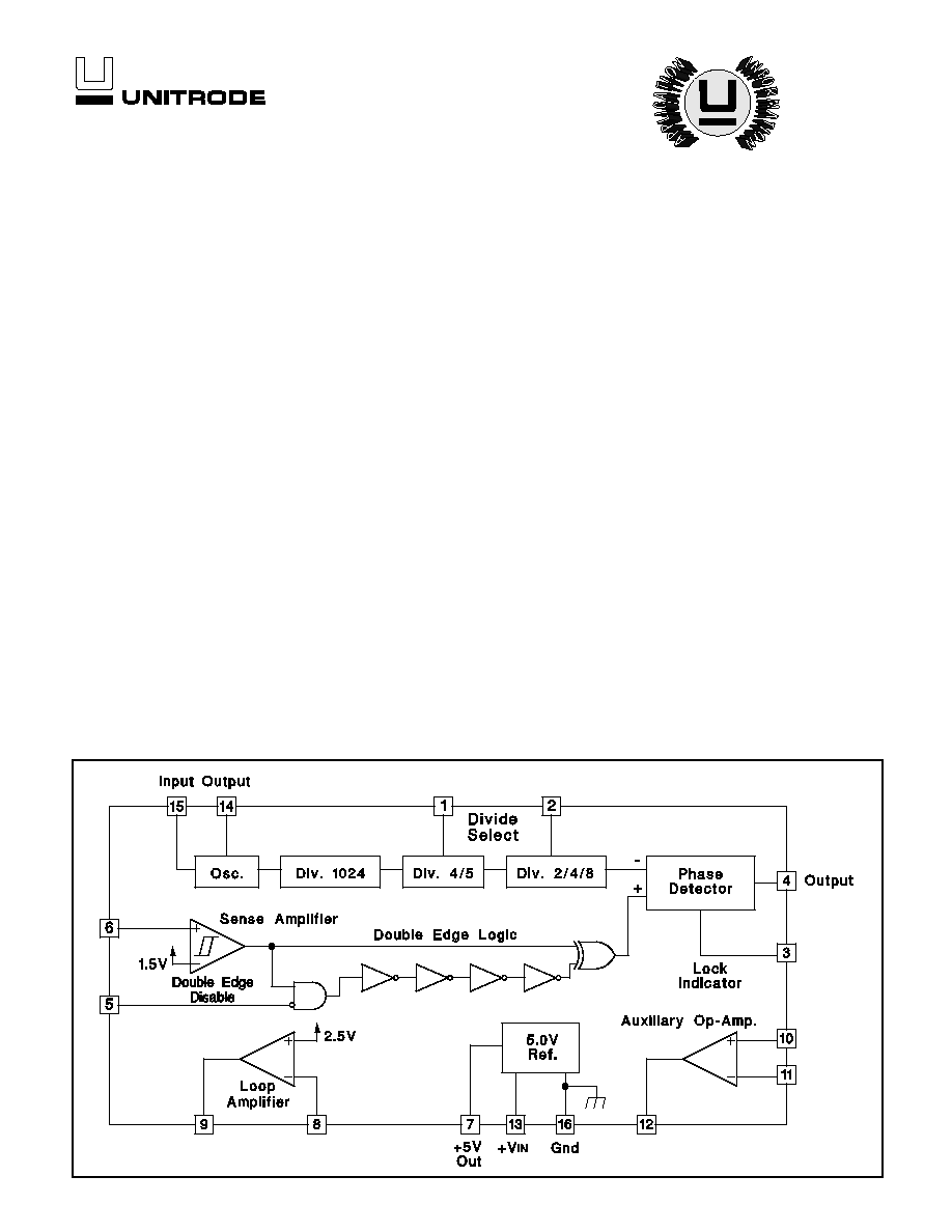
DESCRIPTION
BLOCK DIAGRAM
1

PARAMETER
TEST CONDITIONS
MIN.
TYP.
MAX. UNITS
Supply Current
+V
IN
= 15V
20
28
mA
Reference
Output Voltage (V
REF
)
4.75
5.0
5.25
V
Load Regulation
I
OUT
= 0V to 7mA
5.0
20
mV
Line Regulation
+V
IN
= 8V to 15V
2.0
20
mV
Short Circuit Current
V
OUT
= 0V
12
30
mA
Oscillator
DC Voltage Gain
Oscillator Input to Oscillator Output
12
16
20
dB
Input DC Level (V
IB
)
Oscillator Input Pin Open, T
J
= 25∞C
1.15
1.3
1.45
V
Input Impedance (Note 3)
V
IN
= V
IB
±
0.5V, T
J
= 25
∞
C
1.3
1.6
1.9
k
Output DC Level
Oscillator Input Pin Open, T
J
= 25∞C
1.2
1.4
1.6
V
Maximum Operating Frequency
10
MHz
Dividers
Maximum Input Frequency
Input = 1V
PP
at Oscillator Input
10
MHz
Div. 4/5 Input Current
Input = 5V (Div. by 4)
150
500
µ
A
Input = 0V (Div. by 5)
-5.0
0.0
5.0
µ
A
Div. 4/5 Threshold
0.5
1.6
2.2
V
Note 3: These impedence levels will vary with T
J
at about 1700ppm/∞C
UC1633
UC2633
UC3633
Input Supply Voltage (+V
IN
) . . . . . . . . . . . . . . . . . . . . . . . . +20V
Reference Output Current . . . . . . . . . . . . . . . . . . . . . . . . -30mA
Op-Amp Output Currents . . . . . . . . . . . . . . . . . . . . . . . .
±
30mA
Op-Amp Input Voltages . . . . . . . . . . . . . . . . . . . . . -.3V to +20V
Phase Detector Output Current . . . . . . . . . . . . . . . . . . .
±
10mA
Lock Indicator Output Current . . . . . . . . . . . . . . . . . . . . +15mA
Lock Indicator Output Voltage . . . . . . . . . . . . . . . . . . . . . . +20V
Divide Select Input Voltages . . . . . . . . . . . . . . . . . -.3V to +10V
Double Edge Disable Input Voltage . . . . . . . . . . . . -.3V to +10V
Oscillator Input Voltage . . . . . . . . . . . . . . . . . . . . . . -.3V to +5V
Sense Amplifier Input Voltage . . . . . . . . . . . . . . . . .3V to +20V
Power Dissipation at T
A
= 25∞C (Note 2 . . . . . . . . . . . 1000mW
Power dissipation at T
C
= 25∞C (Note 2) . . . . . . . . . . . 2000mW
Operating Junction Temperature . . . . . . . . . . . -55∞C to +150∞C
Storage Temperature . . . . . . . . . . . . . . . . . . . . -65∞C to +150∞C
Lead Temperature (Soldering, 10 Seconds) . . . . . . . . . . 300∞C
ABSOLUTE MAXIMUM RATINGS
CONNECTION DIAGRAMS
PACKAGE PIN FUNCTION
FUNCTION
PIN
N/C
1
Div 4/5 Input
2
Div 2/4/8 Input
3
Lock Indicator Output
4
Phase Detector Output
5
N/C
6
Dbl Edge Disable Input
7
Sense Amp Input
8
5V Ref Output
9
Loop Amp Inv Input
10
N/C
11
Loop Amp Output
12
Aux Amp Non-Inv Input
13
Aux Amp Inv Input
14
Aux Amp Output
15
N/C
16
+V
IN
17
OSC Output
18
OSC Input
19
Ground
20
PLCC-20 (TOP VIEW)
Q Package
Note1: Voltages are referenced to ground, (Pin 16). Currents
are positive into, negative out of, the specified terminals.
Note 2: Consult Packaging Section of Databook for thermal limi-
tations and considerations of package.
DIL-16 (TOP VIEW)
J or N Package
ELECTRICAL CHARACTERISTICS:
(Unless otherwise stated, these specifications apply for T
A
= 0∞C to +70∞C for the
UC3633, -25
∞
C to +85
∞
C for the UC2633, -55∞C to +125∞C for the UC1633, +V
IN
=
12V; T
A
=T
J
.)
2

PARAMETER
TEST CONDITIONS
MIN.
TYP.
MAX. UNITS
Dividers (cont.)
Div. 2/4/8 Input Current
Input = 5V (Div. by 8)
150
500
µ
A
Input = 0V (Div. by 2)
-500
-150
µ
A
Div. 2/4/8 Open Circuit Voltage
Input Current = 0
µ
A (Div. by 4)
1.5
2.5
3.5
V
Div. by 2 Threshold
0.20
0.8
V
Div. by 4 Threshold
1.5
3.5
V
Div. by 8 Threshold
Volts Below V
REF
0.20
0.8
V
Sense Amplifier
Threshold Voltage
Percent of V
REF
27
30
33
%
Threshold Hysteresis
10
mV
Input Bias Current
Input = 1.5V
-1.0
-0.2
µ
A
Double Edge Disable Input
Input Current
Input = 5V (Disabled)
150
500
µ
A
Input = 0V (Enabled)
-5.0
0.0
5.0
µ
A
Threshold Voltage
0.5
1.6
2.2
v
Phase Detector
High Output Level
Positive Phase/Freq. Error, Volts Below V
REF
0.2
0.5
V
Low Output Level
Negative Phase/Freq. Error
0.2
0.5
V
Mid Output Level
Zero Phase/Freq. Error, Percent of V
REF
47
50
53
%
High Level Maximum Source Current
V
OUT
= 4.3V
2.0
8.0
mA
Low Level Maximum Sink Current
V
OUT
= 0.7V
2.0
5.0
mA
Mid Level Output Impedance (Note 3)
I
OUT
= -200 to +200
µ
A, T
J
= 25∞C
4.5
6.0
7.5
k
Lock Indicator Output
Saturation Voltage
Freq. Error, I
OUT
= 5mA
0.3
0.45
V
Leakage Current
Zero Freq. Error, V
OUT
= 15V
0.1
1.0
µ
A
Loop Amplifier
NON INV. Reference Voltage
Percent of V
REF
47
50
53
%
Input Bias Current
Input = 2.5V
-0.8
-0.2
µ
A
AVOL
60
75
dB
PSRR
+V
IN
= 8V to 15V
70
100
dB
Short Circuit Current
Source, V
OUT
= 0V
16
35
mA
Sink, V
OUT
= 5V
16
30
mA
Auxiliary Op-Amp
Input Offset Voltage
V
CM
= 2.5V
8
mV
Input Bias Current
V
CM
= 2.5V
-0.8
-0.2
µ
A
Input Offset Current
V
CM
= 2.5V
.01
0.1
µ
A
AVOL
70
120
dB
PSRR
+V
IN
= 8V to 15V
70
100
dB
CMRR
V
CM
= 0V to 10V
70
100
dB
Short Circuit Current
Source, V
OUT
= 0V
16
35
mA
Sink, V
OUT
= 5V
16
30
mA
Note 3: These impedence levels will vary with T
J
at about 1700ppm/∞C
UC1633
UC2633
UC3633
ELECTRICAL
CHARACTERISTICS (cont.):
(Unless otherwise stated, these specifications apply for T
A
= 0∞C to +70∞C for the UC3633,
-25
∞
C to +85
∞
C for the UC2633, -55∞C to +125∞C for the UC1633, +V
IN
= 12V; T
A
=T
J
.)
3
UC1633
UC2633
UC3633
Determining the Oscillator Frequency
The frequency at the oscillator is determined by the de-
sired RPM of the motor, the divide ratio selected, the
number of poles in the motor, and the state of the double
edge select pin.
f
OSC
(Hz) = (Divide Ratio)
∑
(Motor RPM)
∑
(1/60 SEC/MIN)
∑
(No. of Rotor Poles/2)
∑
(x 2 if Pin 5 Low)
The resulting reference frequency appearing at the phase
detector inputs is equal to the oscillator frequency divided
by the selected divide ratio. If the double edge option is
used, (Pin 5 low), the frequency of the sense amplifier in-
put signal is doubled by responding to both the rising and
falling edges of the input signal. Using this option, the loop
reference frequency can be doubled for a given motor
RPM.
APPLICATION AND OPERATING INFORMATION
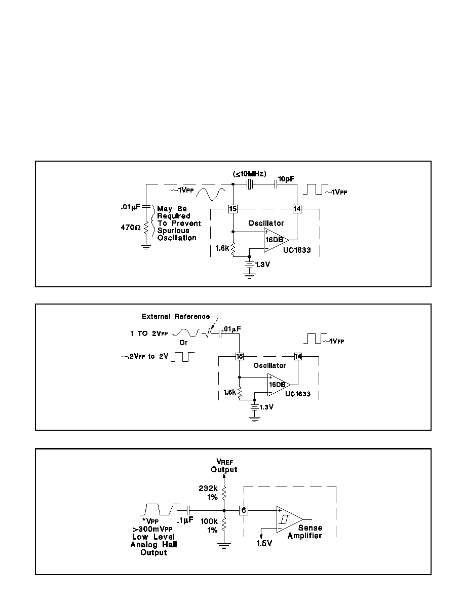
Recommended Oscillator Configuration Using AT Cut Quartz Crystal
External Reference Frequency Input
Method for Deriving Rotation Feedback Signal from Analog Hall Effect Device
*This signal may require filtering if chopped mode drive scheme is used.
4
Phase Detector Operation
The phase detector on these devices is a digital circuit
that responds to the rising edges of the detector's two in-
puts. The phase detector output has three states: a high,
5V state, a low, 0V state, and a middle, 2.5V state. In the
high and low states the output impedance of the detector
is low and the middle state output impedence is high, typi-
cally 6.0k
. When there is any static frequency difference
between the inputs, the detector output is fixed at its high
level if the +input (the sense amplifier signal) is greater in
frequency, and fixed at its low level if the -input (the refer-
ence frequency signal) is greater in frequency.
When the frequencies of the two inputs to the detector
are equal, the phase detector switches between its middle
state and either the high or low states, depending on the
relative phase of the two signals. If the +input is leading in
phase then, during each period of the input frequency, the
detector output will be high for a time equal to the time dif-
ference between the rising edges of the inputs, and will
be at its middle level for the remainder of the period. If the
phase relationship is reversed, then the detector will go
low for a time proportional to the phase difference of the
inputs. The resulting gain of the phase detector. k¯, is
5V/4
radians or about 0.4V/radian. The dynamic range of
the detector is
±
2
radians.
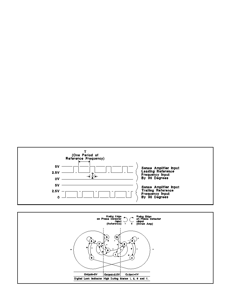
The operation of the phase detector is illustrated in the
figures below. The upper figure shows typical voltage
waveforms seen at the detector output for leading and
lagging phase conditions. The lower figure is a state dia-
gram of the phase detector logic. In this figure, the circles
represent the 10 possible states of the logic, and the con-
necting arrows represent the transition events/paths to
and from these states. Transition arrows that have a clock-
wise rotation are the result of a rising edge on the +input,
and conversely, those with counter-clockwise rotation are
tied to the rising edge of the -input signal.
The normal operational states of the logic are 6 and 7 for
positive phase error, 1 and 2 for a negative phase error.
States 8 and 9 occur during positive frequency error, 3
and 4 during negative frequency error. States 5 and 10
occur only as the inputs cross over from the frequency er-
ror to a normal phase error only condition. The level of the
phase detector output is determined by the logic state as
defined in the state diagram figure. The lock indicator out-
put is high, off, when the detector is in states 1, 2, 6, or 7.
UC1633
UC2633
UC3633
Typical Phase Detector Output Waveforms
Phase Detector State Diagram
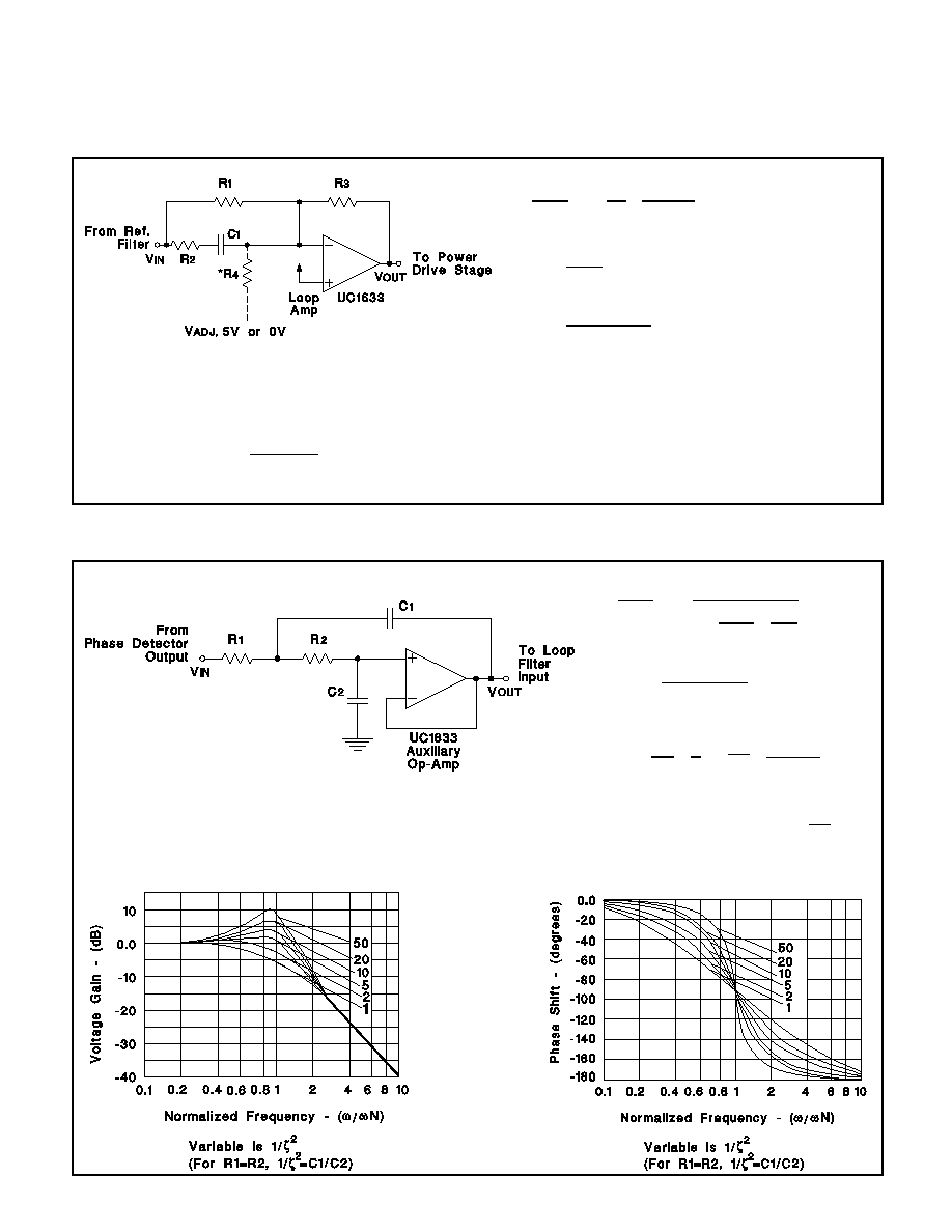
APPLICATION AND OPERATION INFORMATION
5
UC1633
UC2633
UC3633
APPLICATION AND OPERATION INFORMATION
OUT
IN
(
s
)
=
R
3
R
1
∑
1
+
s
/
z
1
+
s
/
p
p
=
1
R
2
C
1
z
=
1
(
R
1
+
R
2
)
C
1
Where: |
V
OUT
| = |V
OUT
- 2.5V|
and V
OUT
= DC Operating Voltage At
Loop Amplifier Output During Phase Lock
If:
(V
OUT
- 2.5) > 0, R
4
Goes to 0V
(V
OUT
- 2.5) < 0, R
4
Goes to 5.0V
* The static phase error of the loop is easily adjusted by
adding resistor, R
4
, as shown. To lock at zero phase error
R
4
is determined by:
R
4
=
2.5V
∑
R
3
|
V
OUT
|
OUT
IN
(
s
)
=
1
1
+
s
2
N
+
s
2
N
2
N
=
1
R
1
R
2
C
1
C
2
=
1
2Q
=
1
2
C
2
C
1
R
1
+
R
2
R
1
R
2
Note: with R
1
= R
2
,
=
C
2
C
1
Reference Filter Design Aid - Gain Response
Reference Filter Design Aid - Phase Response
Reference Filter Configuration
Suggested Loop Filter Configuration
6
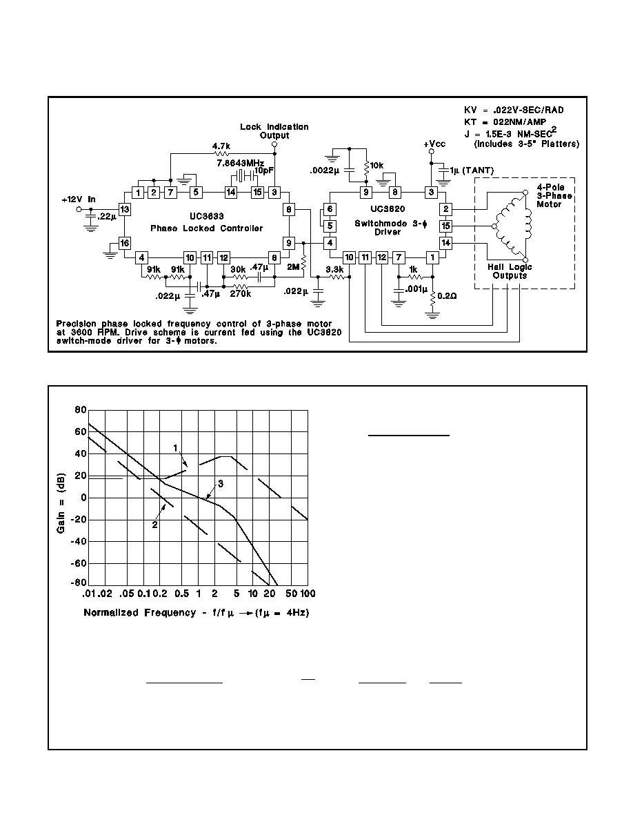
Design Example
UC1633
UC2633
UC3633
Bode Plots - Design Example Open Loop Response
1.)
K
LF
(s)
∑
K
RF
(s)
2.*)
N
∑
K
∑
G
PD
∑
K
T
s
2
∑
J
3.) Combined Overall Open Loop Response
Where:
K
LF
(s) = Loop Filter Response
K
RF
(s) = Reference Filter Response
N = 4 (Using Double Edge Sensing With 4 Pole
Motor)
K
= Phase Detector Gain (.4V/RAD)
G
PD
= Power Stage Transductance (1A/V)
K
T
= Motor Torque Constant (.022NM/A)
J = Motor Moment of Inertia (.0015NM/A - SEC
2
)
s = 2
jf
*Note: For a current mode driver the electrical time constant, L
M
/ R
M,
of the motor does not enter into the small signal response.
If a voltage mode drive scheme is used, then the asymptote, plotted as 2 above, can be approximated by:
N
∑
K
∑
K
PD
∑
K
T
s
2
∑
J
∑
R
M
if: R
M
>
K
T
L
M
J
and,
K
T
2
2
∑
J
∑
R
M
<
f <
R
M
2
∑
L
M
Here: K
PD
= Voltage gain of Driver Stage
R
M
= Motor Winding Resistance
L
M
= Motor Winding Inductance
APPLICATION AND OPERATION INFORMATION
UNITRODE CORPORATION
7 CONTINENTAL BLVD.
∑
MERRIMACK, NH 03054
TEL. (603) 424-2410
∑
FAX (603) 424-3460
7

IMPORTANT NOTICE
Texas Instruments and its subsidiaries (TI) reserve the right to make changes to their products or to discontinue
any product or service without notice, and advise customers to obtain the latest version of relevant information
to verify, before placing orders, that information being relied on is current and complete. All products are sold
subject to the terms and conditions of sale supplied at the time of order acknowledgement, including those
pertaining to warranty, patent infringement, and limitation of liability.
TI warrants performance of its semiconductor products to the specifications applicable at the time of sale in
accordance with TI's standard warranty. Testing and other quality control techniques are utilized to the extent
TI deems necessary to support this warranty. Specific testing of all parameters of each device is not necessarily
performed, except those mandated by government requirements.
CERTAIN APPLICATIONS USING SEMICONDUCTOR PRODUCTS MAY INVOLVE POTENTIAL RISKS OF
DEATH, PERSONAL INJURY, OR SEVERE PROPERTY OR ENVIRONMENTAL DAMAGE ("CRITICAL
APPLICATIONS"). TI SEMICONDUCTOR PRODUCTS ARE NOT DESIGNED, AUTHORIZED, OR
WARRANTED TO BE SUITABLE FOR USE IN LIFE-SUPPORT DEVICES OR SYSTEMS OR OTHER
CRITICAL APPLICATIONS. INCLUSION OF TI PRODUCTS IN SUCH APPLICATIONS IS UNDERSTOOD TO
BE FULLY AT THE CUSTOMER'S RISK.
In order to minimize risks associated with the customer's applications, adequate design and operating
safeguards must be provided by the customer to minimize inherent or procedural hazards.
TI assumes no liability for applications assistance or customer product design. TI does not warrant or represent
that any license, either express or implied, is granted under any patent right, copyright, mask work right, or other
intellectual property right of TI covering or relating to any combination, machine, or process in which such
semiconductor products or services might be or are used. TI's publication of information regarding any third
party's products or services does not constitute TI's approval, warranty or endorsement thereof.
Copyright
©
1999, Texas Instruments Incorporated