Document Outline
- Application Notes
- Design Notes
∑
Receives Power and Signal from Single
Isolation Transformer
∑
Generates Split Rail for 4A Peak Bipolar
Gate Drive
∑
16V High Level Gate Drive
∑
Low Level Gate Drive more Negative
than -5V
∑
Undervoltage Lockout
∑
Desaturation Detection and Fault
Processing
∑
Separate Output Enable Input
∑
Programmable Stepped Gate Drive for
Soft Turn On
∑
Programmable Stepped Gate Drive for
Soft Fault
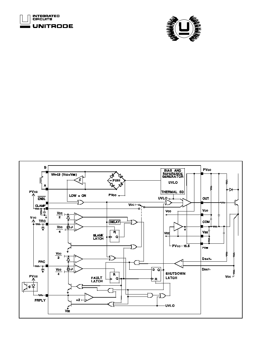
The UC1727 and its companion chip, the UC1726, provide all the
necessary features to drive an isolated IGBT transistor from a TTL in-
put signal. A unique modulation scheme is used to transmit both
power and signal across an isolation boundary with a minimum of ex-
ternal components.
Protection features include under voltage lockout and desaturation
detection. High level gate drive signals are typically 16V. Intermediate
high drive levels can be programmed for various periods of time to
limit surge current at turn on and in the event of desaturation due to a
short circuit.
The chip generates a bipolar supply so that the gate can be driven to
a negative voltage insuring the IGBT remains off in the presence of
high common mode slew rates.
Uses include isolated off-line full bridge and half bridge drives for mo-
tors, switches, and any other load requiring full electrical isolation.
Isolated High Side IGBT Driver
FEATURES DESCRIPTION
BLOCK DIAGRAM
UC1727
UC2727
UC3727
12/94
UDG-94005-2
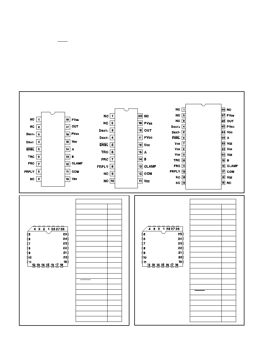
CONNECTION DIAGRAMS
PACKAGE PIN FUNCTION
FUNCTION
PIN
N/C
1
V
EE
2
N/C
3-4
COM
5
CLAMP
6
B
7
A
8
V
CC
9
PV
CC
10
OUT
11
PV
EE
12-18
D
SAT+
19
D
SAT-
20
ENBL
21
NC
22
TRC
23
FRC
24
FRPLY
25
N/C
26
N/C
27
N/C
28
PLCC-28 (Top View)
QP Package
LCC-28 (Top View)
LP Package
DIL-20 (Top View)
N Package
UC1727
UC2727
UC3727
Supply voltage (V
CC
- V
EE
). . . . . . . . . . . . . . . . . . . . . . . . . . . . . . . . . . . . . 40V
Power Inputs (|A - B|) . . . . . . . . . . . . . . . . . . . . . . . . . . . . . . . . . . . . . . . . . 45V
Analog Input Voltage (ENBL, CLAMP). . . . . . . . . . . . . . . . . . -0.3 To Vcc+0.3
Analog Input Voltage (D
SAT+
, D
SAT-
) . . . . . . . . . . . . . . . . V
EE
-0.3 to V
CC
+0.3
Analog Input Current (D
SAT+
, D
SAT-
) . . . . . . . . . . . . . . . . . . . . . . -10 to 10mA
Output Current,
(
OUT)
DC . . . . . . . . . . . . . . . . . . . . . . . . . . . . . . . . . . . . . . . . . . . . . . . . . . . . 0.8A
Pulse (0.5
µ
s) . . . . . . . . . . . . . . . . . . . . . . . . . . . . . . . . . . . . . . . . . . . . . . 4A
FRPLY Output Current . . . . . . . . . . . . . . . . . . . . . . . . . . . . . . . . . . . . . . 30mA
Note: All voltages are with respect to COM. Currents are positive into the
specified terminal.
PACKAGE PIN FUNCTION
FUNCTION
PIN
N/C
1
V
EE
2
N/C
3-4
COM
5
CLAMP
6
B
7
A
8
V
CC
9
PV
CC
10
OUT
11
N/C
12-13
PV
EE
14
N/C
15-18
D
SAT+
19
D
SAT-
20
ENBL
21
NC
22
TRC
23
FRC
24
FRPLY
25
N/C
26-28
ABSOLUTE MAXIMUM RATINGS
DIL-18 (Top View)
J Package
SOIC-28 (Top View)
DWP Package
2
ELECTRICAL CHARACTERISTICS:
PIN DESCRIPTIONS
A, B: Signal and power input pins. Connect these pins to
the secondary of the transformer driven by UC1726.
CLAMP: Analog programming pin for intermediate drive
level to be used at turn on or in response to a desatura-
tion event. Requires a bypass capacitor to COM.
COM: Self generated common for bipolar supply. This
pin will be 16.5V below PV
CC
.
D
SAT+
, D
SAT-
: Inputs to the desaturation comparator. De-
saturation is detected when D
SAT+
is greater than D
SAT-
.
ENBL: Negative true enable input. Tie to V
CC
to disable
the chip. Connect to COM to enable the chip. If the ENBL
pin is used as the primary input to the chip, connect B to
V
CC
and A to V
EE
.
FRC: Fault Resistor and Capacitor. Programs the dura-
tion that OUT will be held at CLAMP potential during a de-
saturation event before it is driven fully low. Also sets the
period of time that OUT will be held low before allowing it
to be driven high again.
FRPLY: Fault Reply pin. Open collector output. Normally
connected to V
EE
. When desaturation is detected, the pin
opens.
OUT: Gate drive output. Connect to gate of IGBT with a
series damping resistor greater than 3 ohms.
TRC: Timing Resistor and Capacitor. Programs the dura-
tion that OUT will be held at CLAMP potential and the pe-
riod of time the desaturation comparator will be ignored
during the rising edge.
V
CC
: Positive supply voltage. Bypass to COM with a low
ESL/ESR 1
µ
F capacitor.
V
EE
: Negative supply voltage. Bypass to COM with a low
ESL/ESR 1
µ
F capacitor.
PV
EE
: Output driver negative supply. Connect to V
EE
with a 3.3 ohm resistor and bypass to COM with a low
ESL/ESR 1
µ
F capacitor.
PV
CC
: Output driver positive supply. Connect to V
CC
with
a 3.3 ohm resistor and bypass to COM with a low
ESL/ESR 1
µ
F capacitor.
PARAMETER
TEST CONDITIONS
MIN
TYP
MAX
UNITS
Power Input Receivers
Forward Diode Drop
I
F
= 50mA
0.5
0.65
V
I
F
= 500mA
1.2
2
V
V
CC
Regulator
V
CC
25
(V
CC
- V
EE
)
36V,
I(COM)
15mA
15.5
16.5
17.5
V
Hysteresis Comparator
Input Open Circuit Voltage
(Measured with respect to V
EE
)
12
V
Input Impedance
100
k
Hysteresis
44
47
50
V
Enable Input
High Level Input Voltage
12
V
Low Level Input Voltage
5
V
Input Bias Current
ENBL = COM
-
460
-
900
µ
A
Output Driver
Saturation to V
CC
I(OUT) = -20mA
1.7
2.3
V
Saturation to V
CC
I(OUT) = -500mA
2
2.5
V
Saturation to V
EE
I(OUT) = 20mA
2
3
V
Saturation to V
EE
I(OUT) = 500mA
2.4
3.6
V
Unless otherwise stated, these specifications apply for T
A
=
-
55
∞
C to 125
∞
C for the
UC1727, T
A
=
-
40
∞
C to 85
∞
C for the UC2727, T
A
= 0
∞
C to 70
∞
C for the UC3727,
R(TRC) = 54.9k, C(TRC) = 180pF, R(FRC) = 309K, C(FRC) = 200pF, V
CC
- V
EE
=
25V, CLAMP = 9V, T
A
= T
J,
and all voltages are measured with respect to COM.
UC1727
UC2727
UC3727
See Application Note U-143A "New Chip Pair Provides Isolated Drive for High Voltage IGBTs"
3
PARAMETER
TEST CONDITIONS
MIN
TYP
MAX
UNITS
Output Driver (cont.)
Turn on Clamp Voltage
I(OUT) = -100mA
7
9
11
V
Fault Clamp Voltage
|I(OUT)| = 100mA
8
10
12.5
V
UVLO Saturation to V
EE
I(OUT) = 20mA,V
CC
no connection
2
3
V
Rise and Fall Times
Cl = 1n, CLAMP = V
CC
, R
OUT
= 3
(Note 1)
75
150
ns
Turn On Sequence Timer
Clamped Driver Time
(Note 1)
0.4
1
1.7
µ
s
Blanking Time
(Note 1)
3
5
7
µ
s
Fault Manager
Clamped Driver Time
(Note 1)
0.4
1
1.7
µ
s
Fault Lock Off Time
(Note 1)
15
25
35
µ
s
FRPLY Saturation
I(FRPLY) = 10mA
1.8
3
V
FRPLY Leakage
FRPLY = V
CC
0
10
µ
A
Desaturation Detection Comparator
Input Offset Voltage (|vio|)
V
CM
= V
EE
+2, V
CM
= V
CC
-2
0
20
mV
Input Bias Current
-
1.5
10
µ
A
Delay to Output
C(FRC) = 0 (Note 1)
150
ns
Undervoltage Lock Out
V
CC
Threshold
14
15.5
17
V
V
CC
Hysteresis
0.35
V
V
EE
Threshold
-4.
5
-
5.5
-
6.5
V
V
EE
Hysteresis
0.5
1
1.5
V
Thermal Shutdown
Threshold
Not tested
175
∞
C
Hysteresis
Not tested
45
∞
C
Total Standby Current
I(V
CC
)
24
30
mA
Unless otherwise stated, these specifications apply for T
A
=
-
55
∞
C to 125
∞
C for the
UC1727, T
A
=
-
40
∞
C to 85
∞
C for the UC2727, T
A
= 0
∞
C to 70
∞
C for the UC3727,
R(TRC) = 54.9k, C(TRC) = 180pF, R(FRC) = 309K, C(FRC) = 200pF, V
CC
- V
EE
=
25V, CLAMP = 9V, T
A
= T
J,
and all voltages are measured with respect to COM.
ELECTRICAL CHARACTERISTICS:
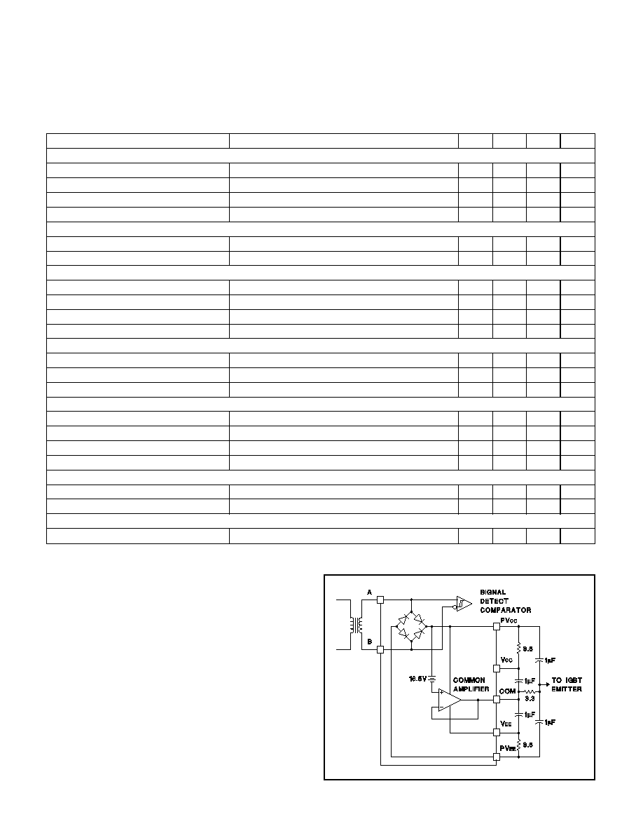
APPLICATION INFORMATION
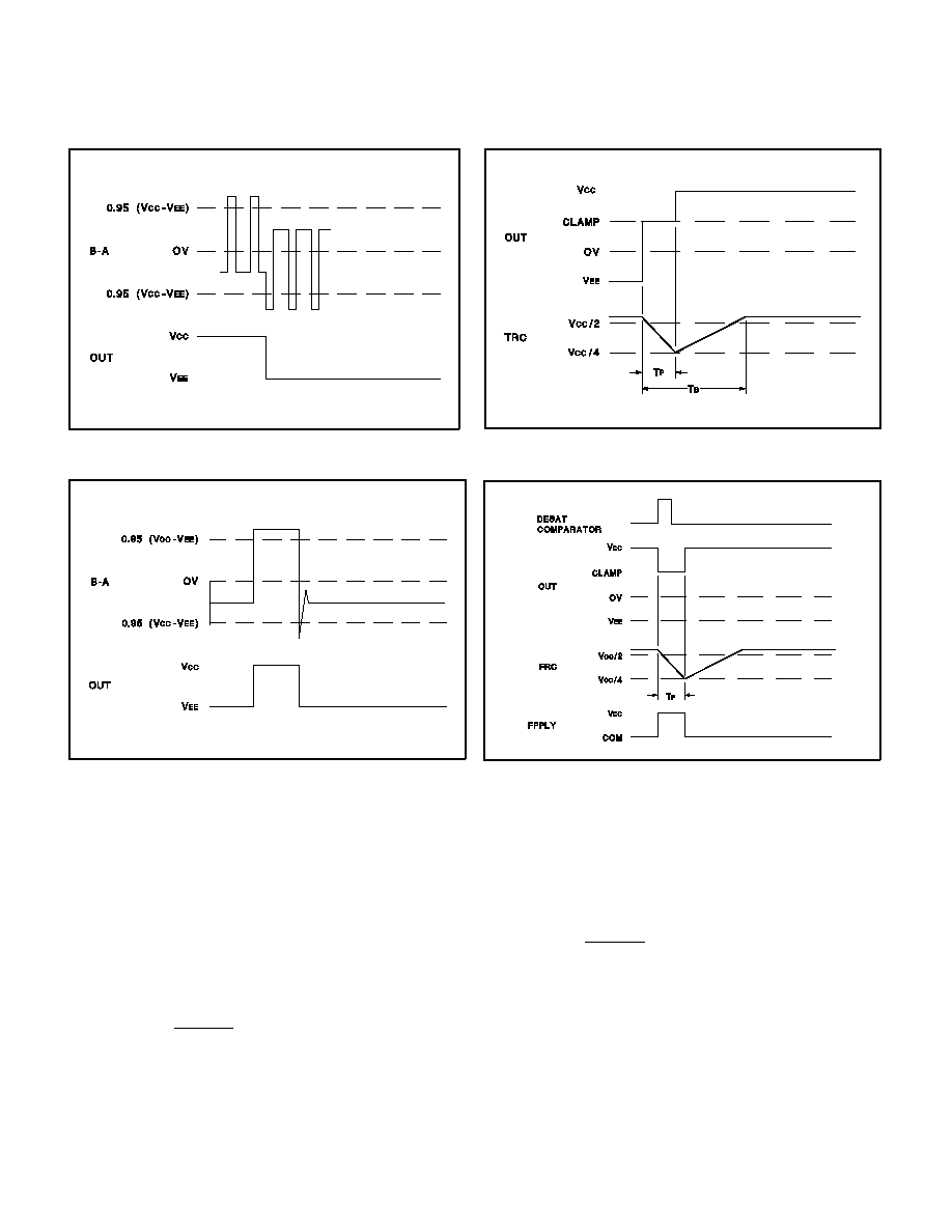
Figure 1 shows the rectification and detection scheme
used in the UC1727 to derive both power and signal infor-
mation from the input waveform. V
CC
-V
EE
is generated by
peak detecting the input signal via the internal bridge rec-
tifier and storing it on external capacitors. COM is gener-
ated by an internal amplifier that maintains PV
CC
-COM =
16.5V.
Signal detection is performed by the internal hysteresis
comparator which senses the polarity of the input signal
as shown in Figure 2. This is accomplished by setting (or
resetting) the comparator only if the input signal exceeds
0.95
V
CC
-V
EE
. In some cases it may be necessary to
add a damping resistor across the transformer secondary
to minimize ringing and eliminate false triggering of the
hysteresis comparator as shown in Figure 3.
UC1727
UC2727
UC3727
Figure 1.
Input Stage & Bipolar Supply
Note 1: Guaranteed by design, but not 100% tested in production.
4
UC1727
UC2727
UC3727
APPLICATION INFORMATION (cont.)
Figure 4.
Rising Edge Waveform
Figure 5. Transient Desaturation Response
GATE DRIVE WAVEFORM
The rising edge of OUT can be programmed for a two
step sequence as shown in Figure 4. The plateau voltage
is programmed by a resistive divider from V
CC
to COM
applied at CLAMP. CLAMP must be bypassed to COM.
The plateau voltage is approximately OUT = CLAMP. The
plateau time is set by a resistor from TRC to V
CC
and a
capacitor to COM as:
Tp
=
RC ln
R
-
7.6
k
R
-
12.4
k
.
TRC also programs a blanking time during which the chip
ignores the desaturation comparator. The blanking time
is:
Tb = Tp + 0.4RC.
In the event that desaturation is detected outside the
blanking interval, OUT will be driven back to the CLAMP
plateau for a fault time set by a resistor from FRC to V
CC
and a capacitor to COM as:
Tf
=
RC ln
R
-
7.6
k
R
-
12.4
k
.
If the event is transient, OUT will return high at the end of
Tf as shown in Figure 5. During Tf, FRPLY is open. After
Tf, FRPLY is connected to COM.
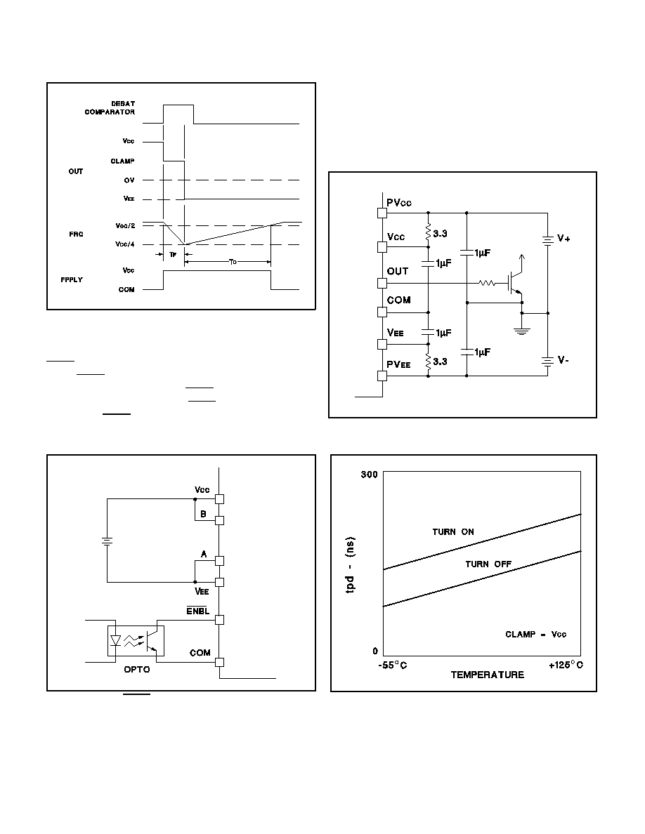
Desaturation shown in Figure 6 that persists longer than
Tf will cause OUT to be driven low. The chip will not ac-
cept a command to drive OUT high for a delay period of
Td = 0.4RC
FRPLY will be open during this entire period.
Figure 2. Input Waveform
Figure 3. Output Pulsing Caused By Transformer Ringing
5
ENABLE
ENBL provides an alternate means of controlling the out-
put. If ENBL is used as the primary input, B must be con-
nected to V
CC
and A to V
EE
. ENBL can be driven by the
output of an optoisolator from ENBL to COM as shown in
Figure 7. If ENBL is not used, it should be connected to
COM.
Figure 7.
Using ENBL as Primary Input
EXTERNAL BIPOLAR SUPPLIES
If it is desired to drive an emitter grounded IGBT from ex-
ternal supplies, the configuration in Figure 8 should be
used. COM should never be connected to ground. V
CC
must be
12V and V
CC
-V
EE
must be
23.5V.
UNITRODE INTEGRATED CIRCUITS
7 CONTINENTAL BLVD.
∑
∑
MERRIMACK, NH 03054
TEL. (603) 424-2410
∑
∑
FAX (603) 424-3460
Figure 8.
Using External Supplies
Figure 9.
Input to Output Delay
UC1727
UC2727
UC3727
Figure 6.
Desaturation Response
6

IMPORTANT NOTICE
Texas Instruments and its subsidiaries (TI) reserve the right to make changes to their products or to discontinue
any product or service without notice, and advise customers to obtain the latest version of relevant information
to verify, before placing orders, that information being relied on is current and complete. All products are sold
subject to the terms and conditions of sale supplied at the time of order acknowledgement, including those
pertaining to warranty, patent infringement, and limitation of liability.
TI warrants performance of its semiconductor products to the specifications applicable at the time of sale in
accordance with TI's standard warranty. Testing and other quality control techniques are utilized to the extent
TI deems necessary to support this warranty. Specific testing of all parameters of each device is not necessarily
performed, except those mandated by government requirements.
CERTAIN APPLICATIONS USING SEMICONDUCTOR PRODUCTS MAY INVOLVE POTENTIAL RISKS OF
DEATH, PERSONAL INJURY, OR SEVERE PROPERTY OR ENVIRONMENTAL DAMAGE ("CRITICAL
APPLICATIONS"). TI SEMICONDUCTOR PRODUCTS ARE NOT DESIGNED, AUTHORIZED, OR
WARRANTED TO BE SUITABLE FOR USE IN LIFE-SUPPORT DEVICES OR SYSTEMS OR OTHER
CRITICAL APPLICATIONS. INCLUSION OF TI PRODUCTS IN SUCH APPLICATIONS IS UNDERSTOOD TO
BE FULLY AT THE CUSTOMER'S RISK.
In order to minimize risks associated with the customer's applications, adequate design and operating
safeguards must be provided by the customer to minimize inherent or procedural hazards.
TI assumes no liability for applications assistance or customer product design. TI does not warrant or represent
that any license, either express or implied, is granted under any patent right, copyright, mask work right, or other
intellectual property right of TI covering or relating to any combination, machine, or process in which such
semiconductor products or services might be or are used. TI's publication of information regarding any third
party's products or services does not constitute TI's approval, warranty or endorsement thereof.
Copyright
©
1999, Texas Instruments Incorporated