UC1823A,B/1825A,B
UC2823A,B/2825A,B
UC3823A,B/3825A,B
DESCRIPTION
The UC3823A & B and the UC3825A & B family of PWM control ICs are
improved versions of the standard UC3823 & UC3825 family. Performance
enhancements have been made to several of the circuit blocks. Error ampli-
fier gain bandwidth product is 12MHz while input offset voltage is 2mV. Cur-
rent limit threshold is guaranteed to a tolerance of 5%. Oscillator discharge
current is specified at 10mA for accurate dead time control. Frequency ac-
curacy is improved to 6%. Startup supply current, typically 100
µ
A, is ideal
for off-line applications. The output drivers are redesigned to actively sink
current during UVLO at no expense to the startup current specification. In
addition each output is capable of 2A peak currents during transitions.
Functional improvements have also been implemented in this family. The
UC3825 shutdown comparator is now a high-speed overcurrent comparator
with a threshold of 1.2V. The overcurrent comparator sets a latch that en-
sures full discharge of the soft start capacitor before allowing a restart.
While the fault latch is set, the outputs are in the low state. In the event of
continuous faults, the soft start capacitor is fully charged before discharge
to insure that the fault frequency does not exceed the designed soft start
period. The UC3825 Clock pin has become CLK/LEB. This pin combines
the functions of clock output and leading edge blanking adjustment and has
been buffered for easier interfacing.
(continued)
High Speed PWM Controller
FEATURES
∑
Improved versions of the
UC3823/UC3825 PWMs
∑
Compatible with Voltage or
Current-Mode Topologies
∑
Practical Operation at Switching
Frequencies to 1MHz
∑
50ns Propagation Delay to Output
∑
High Current Dual Totem Pole
Outputs (2A Peak)
∑
Trimmed Oscillator Discharge Current
∑
Low 100
µ
A Startup Current
∑
Pulse-by-Pulse Current Limiting
Comparator
∑
Latched Overcurrent Comparator With
Full Cycle Restart
SLUS334A - AUGUST 1995 - REVISED NOVEMBER 2000
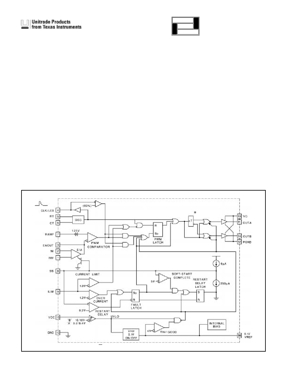
BLOCK DIAGRAM
UDG-95101
* Note: 1823A,B Version Toggles Q and Q are always low
application
INFO
available
2
UC1823A,B/1825A,B
UC2823A,B/2825A,B
UC3823A,B/3825A,B
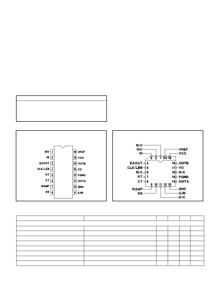
DIL-16, SOIC-16, (Top View)
J or N Package; DW Package
CONNECTION DIAGRAMS
ELECTRICAL CHARACTERISTICS:
Unless otherwise stated, these specifications apply for T
A
= ≠55∞C to +125∞C for
the UC1823A,B and UC1825A,B; ≠40∞C to +85∞C for the UC2823A,B and UC2825A,B; 0∞C to +70∞C for the UC3823A,B and
UC3825A,B; RT = 3.65k, CT = 1nF, VCC = 12V, T
A
= T
J.
PARAMETER
TEST CONDITIONS
MIN
TYP
MAX
UNITS
Reference Section
Output Voltage
T
J
= 25∞C, Io = 1mA
5.05
5.1
5.15
V
Line Regulation
12 < VCC < 20V
2
15
mV
Load Regulation
1mA < I
O
< 10mA
5
20
mV
Total Output Variation
Line, Load, Temp
5.03
5.17
V
Temperature Stability
T
MIN
< T
A
< T
MAX
(Note 1)
0.2
0.4
mV/∞C
Output Noise Voltage
10Hz < f < 10kHz (Note 1)
50
µ
VRMS
Long Term Stability
T
J
= 125∞C, 1000 hours (Note 1)
5
25
mV
Short Circuit Current
VREF = 0V
30
60
90
mA
The UC3825A,B has dual alternating outputs and the
same pin configuration of the UC3825. The UC3823A,B
outputs operate in phase with duty cycles from zero to
less than 100%. The pin configuration of the UC3823A,B
is the same as the UC3823 except pin 11 is now an out-
put pin instead of the reference pin to the current limit
comparator. "A" version parts have UVLO thresholds
identical to the original UC3823/25. The "B" versions
have UVLO thresholds of 16 and 10V, intended for ease
of use in off-line applications.
Consult Application Note U-128 for detailed technical
and applications information. Contact the factory for fur-
ther packaging and availability information.
DESCRIPTION (cont.)
ABSOLUTE MAXIMUM RATINGS
Supply Voltage (VC, VCC) . . . . . . . . . . . . . . . . . . . . . . . . . 22V
Output Current, Source or Sink (Pins OUTA, OUTB)
DC . . . . . . . . . . . . . . . . . . . . . . . . . . . . . . . . . . . . . . . . . 0.5A
Pulse (0.5
µ
s) . . . . . . . . . . . . . . . . . . . . . . . . . . . . . . . . . 2.2A
Power Ground (PGND). . . . . . . . . . . . . . . . . . . . . . . . . . . ±0.2V
Analog Inputs
(INV, NI, RAMP) . . . . . . . . . . . . . . . . . . . . . . . . . ≠0.3V to 7V
(ILIM, SS) . . . . . . . . . . . . . . . . . . . . . . . . . . . . . . ≠0.3V to 6V
Clock Output Current (CLK/LEB) . . . . . . . . . . . . . . . . . . . ≠5mA
Error Amplifier Output Current (EAOUT) . . . . . . . . . . . . . . 5mA
Soft Start Sink Current (SS) . . . . . . . . . . . . . . . . . . . . . . . 20mA
Oscillator Charging Current (RT) . . . . . . . . . . . . . . . . . . . ≠5mA
Power Dissipation at T
A
= 60∞C . . . . . . . . . . . . . . . . . . . . . . 1W
Storage Temperature Range . . . . . . . . . . . . . ≠65∞C to +150∞C
Junction Temperature . . . . . . . . . . . . . . . . . . . ≠55∞C to +150∞C
Lead Temperature (Soldering, 10 sec.) . . . . . . . . . . . . . . 300∞C
All currents are positive into, negative out of the specified ter-
minal. Consult Packaging Section of Databook for thermal limi-
tations and considerations of packages.
PLCC-20, LCC-20, (Top View)
Q, L Packages
Device
UVLO
Dmax
UC3823A
9.2V/8.4V
< 100%
UC3823B
16V/10V
< 100%
UC3825A
9.2V/8.4V
< 50%
UC3825B
16V/10V
< 50%
3
UC1823A,B/1825A,B
UC2823A,B/2825A,B
UC3823A,B/3825A,B
ELECTRICAL CHARACTERISTICS:
Unless otherwise stated, these specifications apply for T
A
= ≠55∞C to +125∞C for
the UC1823A,B and UC1825A,B; ≠40∞C to +85∞C for the UC2823A,B and UC2825A,B; 0∞C to +70∞C for the UC3823A,B and
UC3825A,B; RT = 3.65k, CT = 1nF, VCC = 12V, T
A
= T
J.
PARAMETER
TEST CONDITIONS
MIN
TYP
MAX
UNITS
Oscillator Section
Initial Accuracy
T
J
= 25∞C (Note 1)
375
400
425
kHz
Total Variation
Line, Temperature (Note 1)
350
450
kHz
Voltage Stability
12V < VCC < 20V
1
%
Temperature Stability
T
MIN
< T
A
< T
MAX
(Note 1)
5
%
Initial Accuracy
RT = 6.6k, CT = 220pF, T
A
= 25∞C (Note 1)
0.9
1
1.1
MHz
Total Variation
RT = 6.6k, CT = 220pF (Note 1)
0.85
1.15
MHz
Clock Out High
3.7
4
V
Clock Out Low
0
0.2
V
Ramp Peak
2.6
2.8
3
V
Ramp Valley
0.7
1
1.25
V
Ramp Valley to Peak
1.6
1.8
2
V
Oscillator Discharge Current
RT = Open, V
CT
= 2V
9
10
11
mA
Error Amplifier Section
Input Offset Voltage
2
10
mV
Input Bias Current
0.6
3
µ
A
Input Offset Current
0.1
1
µ
A
Open Loop Gain
1V < V
O
< 4V
60
95
dB
CMRR
1.5V < V
CM
< 5.5V
75
95
dB
PSRR
12V < VCC < 20V
85
110
dB
Output Sink Current
V
EAOUT
= 1V
1
2.5
mA
Output Source Current
V
EAOUT
= 4V
≠0.5
≠1.3
mA
Output High Voltage
I
EAOUT
= ≠0.5mA
4.5
4.7
5
V
Output Low Voltage
I
EAOUT
= 1mA
0
0.5
1
V
Gain Bandwidth Product
F = 200kHz
6
12
MHz
Slew Rate
(Note 1)
6
9
V/
µ
s
PWM Comparator
RAMP Bias Current
V
RAMP
= 0V
≠1
≠8
µ
A
Minimum Duty Cycle
0
%
Maximum Duty Cycle
85
%
Leading Edge Blanking
R = 2k, C = 470pF
300
375
450
ns
LEB Resistor
V
CLK/LEB
= 3V
8.5
10
11.5
kohm
EAOUT Zero D.C. Threshold
V
RAMP
= 0V
1.1
1.25
1.4
V
Delay to Output
V
EAOUT
= 2.1V, V
RAMP
= 0 to 2V Step (Note 1)
50
80
ns
Current Limit/Start Sequence/Fault Section
Soft Start Charge Current
V
SS
= 2.5V
8
14
20
µ
A
Full Soft Start Threshold
4.3
5
V
Restart Discharge Current
V
SS
= 2.5V
100
250
350
µ
A
Restart Threshold
0.3
0.5
V
ILIM Bias Current
0 < V
ILIM
< 2V
15
µ
A
Current Limit Threshold
0.95
1
1.05
V
4
UC1823A,B/1825A,B
UC2823A,B/2825A,B
UC3823A,B/3825A,B
ELECTRICAL CHARACTERISTICS:
Unless otherwise stated, these specifications apply for T
A
= ≠55∞C to +125∞C for
the UC1823A,B and UC1825A,B; ≠40∞C to +85∞C for the UC2823A,B and UC2825A,B; 0∞C to +70∞C for the UC3823A,B and
UC3825A,B; RT = 3.65k, CT = 1nF, VCC = 12V, T
A
= T
J.
PARAMETER
TEST CONDITIONS
MIN
TYP
MAX
UNITS
Current Limit/Start Sequence/Fault Section (cont.)
Over Current Threshold
1.14
1.2
1.26
V
ILIM Delay to Output
V
ILIM
= 0 to 2V Step (Note 1)
50
80
ns
Output Section
Output Low Saturation
I
OUT
= 20mA
0.25
0.4
V
I
OUT
= 200mA
1.2
2.2
V
Output High Saturation
I
OUT
= 20mA
1.9
2.9
V
I
OUT
= 200mA
2
3
V
UVLO Output Low Saturation
I
O
= 20mA
0.8
1.2
V
Rise/Fall Time
C
L
= 1nF (Note 1)
20
45
ns
UnderVoltage Lockout
Start Threshold
UCX823B and X825B only
16
17
V
Stop Threshold
UCX823B and X825B only
9
10
V
UVLO Hysteresis
UCX823B and X825B only
5
6
7
V
Start Threshold
UCX823A and X825A only
8.4
9.2
9.6
V
UVLO Hysteresis
UCX823A and X825A only
0.4
0.8
1.2
V
Supply Current
Startup Current
VC = VCC = V
TH
(start) ≠0.5V
100
300
µ
A
Icc
28
36
mA
Note 1:Guaranteed by design. Not 100% tested in production.
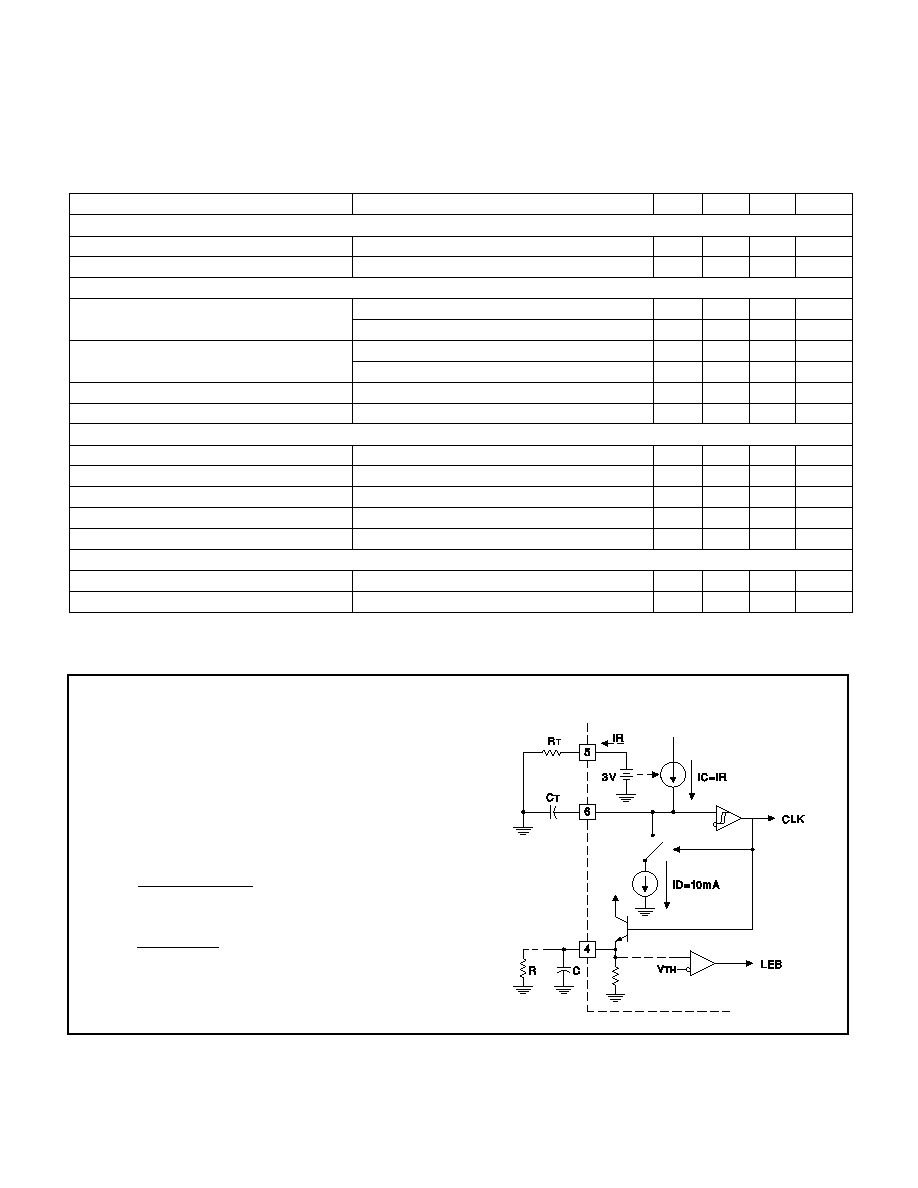
OSCILLATOR
The UC3823A,B/3825A,B oscillator is a saw tooth. The
rising edge is governed by a current controlled by the RT
pin and value of capacitance at the CT pin. The falling
edge of the sawtooth sets dead time for the outputs. Se-
lection of RT should be done first, based on desired
maximum duty cycle. CT can then be chosen based on
desired frequency, RT, and D
MAX
. The design equations
are:
(
)
(
)
RT
V
mA
D
MAX
=
3
10
1 ≠
(
)
(
)
CT
D
RT
F
MAX
=
∑
∑
1 6
.
Recommended values for RT range from 1k to 100k.
Control of D
MAX
less than 70% is not recommended.
Oscillator
APPLICATIONS INFORMATION
UDG-95102
5
UC1823A,B/1825A,B
UC2823A,B/2825A,B
UC3823A,B/3825A,B
OSCILLATOR (cont.)
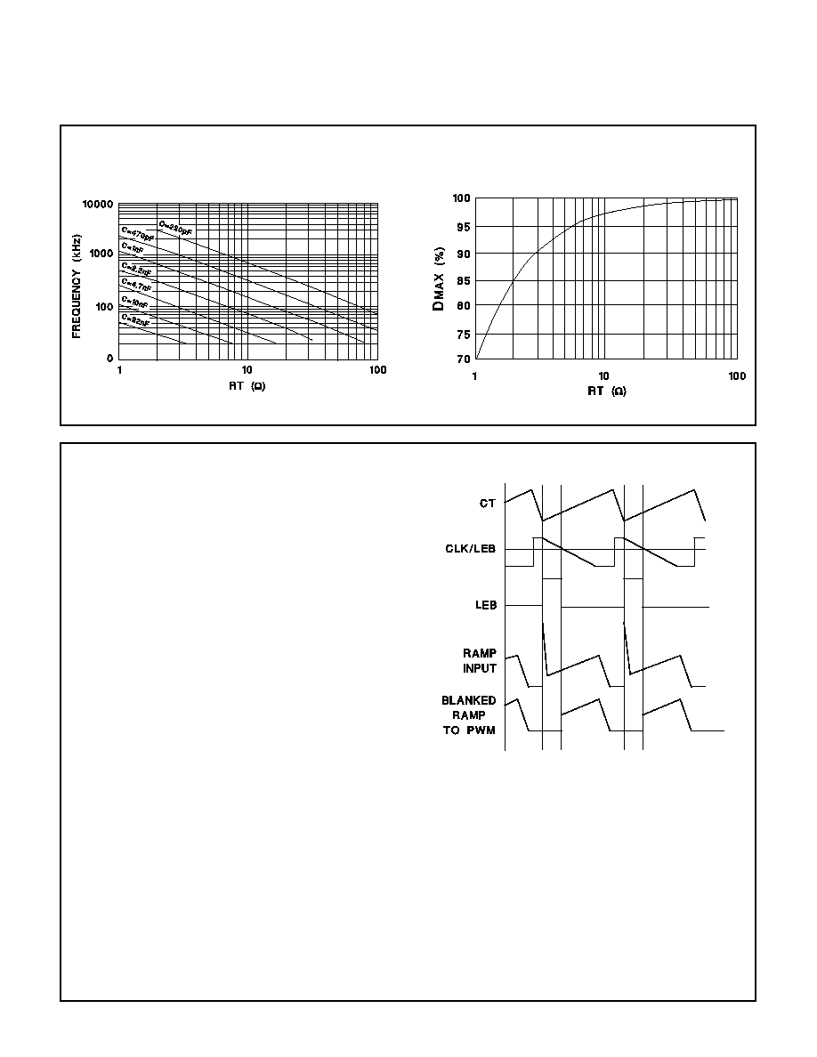
APPLICATIONS INFORMATION (cont.)
Oscillator Frequency vs. R
T
and C
T
Curve
Maximum Duty Cycle vs R
T
Curve
UDG-95104
UDG-95103
LEADING EDGE BLANKING
The UC3823A,B/3825A,B performs fixed frequency
pulse width modulation control. The UC3823A,B out-
puts operate together at the switching frequency and
can vary from 0 to some value less than 100%. The
UC3825A,B outputs are alternately controlled. During
every other cycle, one output will be off. Each output
then, switches at one-half the oscillator frequency, vary-
ing in duty cycle from 0 to less than 50%.
To limit maximum duty cycle, the internal clock pulse
blanks both outputs low during the discharge time of
the oscillator. On the falling edge of the clock, the ap-
propriate output(s) is driven high. The end of the pulse
is controlled by the PWM comparator, current limit com-
parator, or the overcurrent comparator.
Normally the PWM comparator will sense a ramp
crossing a control voltage (error amp output) and termi-
nate the pulse. Leading edge blanking (LEB) causes
the PWM comparator to be ignored for a fixed amount
of time after the start of the pulse. This allows noise in-
herent with switched mode power conversion to be re-
jected. The PWM ramp input may not require any
filtering as result of leading edge blanking.
To program a Leading Edge Blanking period, connect a
capacitor, C, to CLK/LEB. The discharge time set by C
and the internal 10k resistor will determine the blanked
interval. The 10k resistor has a 10% tolerance. For
more accuracy, an external 2k 1% resistor, R, can be
added, resulting in an equivalent resistance of 1.66k
with a tolerance of 2.4%. The design equation is:
t
LEB
= 0.5 ∑ (R | | 10k) ∑ C.
Values of R less than 2k should not be used
Leading edge blanking is also applied to the current
limit comparator. After LEB, if the ILIM pin exceeds the
one volt threshold, the pulse is terminated. The over
current comparator, however, is not blanked. It will
catch catastrophic over current faults without a blanking
delay. Any time the ILIM pin exceeds 1.2V, the fault
latch will be set and the outputs driven low. For this rea-
son, some noise filtering may be required on the ILIM
pin.
LEB Operational Waveforms
UDG-95105