 | –≠–ª–µ–∫—Ç—Ä–æ–Ω–Ω—ã–π –∫–æ–º–ø–æ–Ω–µ–Ω—Ç: UC3838ADW | –°–∫–∞—á–∞—Ç—å:  PDF PDF  ZIP ZIP |

UC2838, UC2838A
UC3838, UC3838A
SLUS221A ≠ APRIL 2000 ≠ REVISED MAY 2001
MAGNETIC AMPLIFIER
CONTROLLER
UDG-97174
10
VCC
VREF
9
2.5 V
REFERENCE
INV. IN
8
E/A OUT
3
INV. IN
6
7
N.I. IN
2
1
N.I. IN
C/L OUT
C/L
E/A
3.5 V
15 DR 1
16 DR 2
RESET
14
VM
11
5
12
13
4
GND GND GND GND
+
≠
+
≠
20
1 k
5 k
1
www.ti.com
FEATURES
D
Independent 1% Reference
D
Two Uncommitted, Identical Operational
Amplifiers
D
100-mA Reset Current Source With ≠120-V
Capability
D
5-V to 40-V Analog Operation
D
5-W DIP Package
BLOCK DIAGRAM
DESCRIPTION
The UC3838 and the UC3838A family of magnetic
amplifier controllers contains the circuitry to
generate and amplify a low-level analog error
signal along with a high voltage-compliant current
source. This source provides the reset current
necessary to enable a magnetic amplifier to
regulate and control a power supply output in the
range of 2 A to 20 A.
The UC3838A originally was a parametric
improvement version of the UC3838 which since
has been used for both versions. There is no
difference between the UC3838A and UC3838
version.
By controlling the reset current to a magnetic
amplifier, this device defines the amount of
volt-seconds the magnetic amplifier blocks before
switching to the conducting state. Magnetic
amplifiers are ideal for post-regulators for
multiple-output power supplies where each output
can be independently controlled with efficiencies
up to 99%. With a square or pulse-width
modulated input voltage, a magnetic amplifier
blocks a portion of this input waveform, allowing
just enough to pass to provide a regulated output.
With the UC3838/A, only the magnetic amplifier
coil, three diodes, and an output L-C filter are
necessary to implement a complete closed-loop
regulator.
AVAILABLE OPTIONS
Packaged Devices
TA = TJ
SOIC Wide
(DW)
PDIP (N)
PLCC (Q)
20
∞
C to 85
∞
C
UC2838DW
UC2838N
UC2838Q
≠20
∞
C to 85
∞
C
UC2838ADW
UC2838AN
UC2838AQ
0
∞
C to 70
∞
C
UC3838DW
UC3838N
UC3838Q
0
∞
C to 70
∞
C
UC3838ADW
UC3838AN
UC3838AQ
PRODUCTION DATA information is current as of publication date.
Products conform to specifications per the terms of Texas Instruments
standard warranty. Production processing does not necessarily include
testing of all parameters.
UC2838, UC2838A
UC3838, UC3838A
SLUS221A ≠ APRIL 2000 ≠ REVISED MAY 2001
2
www.ti.com
description (continued)
The UC3838/A contains a precision 2.5-V reference, two uncommitted high-gain operational amplifier and a
high-gain PNP-equivalent current source which can deliver up to 100 mA of magnetic amplifier reset current
and with ≠120-V capability.
These devices are available in a plastic batwing DIP (N), wide body SOIC (DW), and PLCC (Q) package for
operation over a ≠20
∞
C to 85
∞
C temperature range.
19
20
1
3
2
17
18
16
15
14
13
12
11
9
10
5
4
6
7
8
RESET
N/C
N/C
GND
VM
C/L INV.IN
GND
N/C
N/C
E/A INV.IN
C/LN.I.IN
C/LOUT
N/C
DR2
DR1
E/A
OUT
N/C
VREF
VCC
E/A
N.I.IN
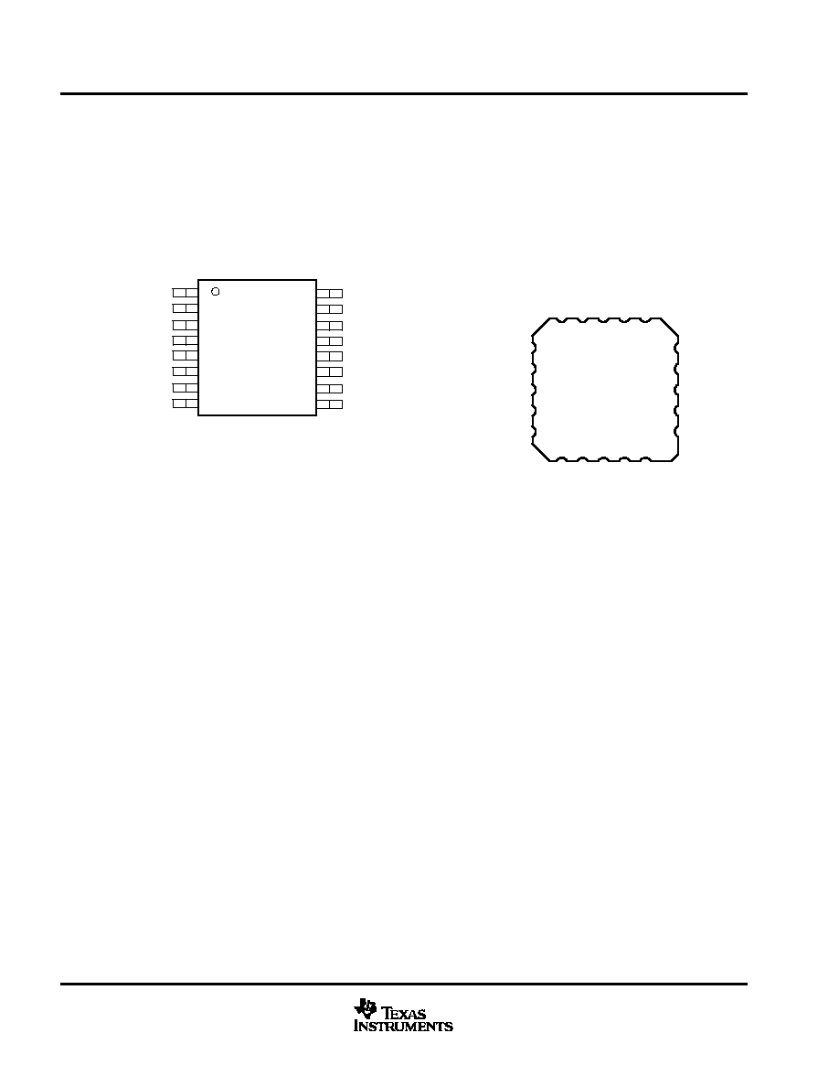
Q PACKAGE
(TOP VIEW)
1
2
3
4
5
6
7
8
16
15
14
13
12
11
10
9
C/L OUT
C/L N.I. IN
C/L INV. IN
GND
GND
E/A INV. IN
E/A N.I. IN
E/A OUT
DR2
DR1
RESET
GND
GND
VM
VCC
VREF
DW AND N PACKAGES
(TOP VIEW)
absolute maximum ratings over operating free-air temperature (unless otherwise noted)
Supply voltage, V
CC
40 V
. . . . . . . . . . . . . . . . . . . . . . . . . . . . . . . . . . . . . . . . . . . . . . . . . . . . . . . . . . . . . . . . . . . . . . . .
Magnetic amplifier source voltage, VM
40 V
. . . . . . . . . . . . . . . . . . . . . . . . . . . . . . . . . . . . . . . . . . . . . . . . . . . . . . . .
Reset output voltage, VR
≠120 V
. . . . . . . . . . . . . . . . . . . . . . . . . . . . . . . . . . . . . . . . . . . . . . . . . . . . . . . . . . . . . . . . . .
Total current source voltage, VM ≠ VR
≠140 V
. . . . . . . . . . . . . . . . . . . . . . . . . . . . . . . . . . . . . . . . . . . . . . . . . . . . . .
Amplifier input range
≠0.3 V to VCC
. . . . . . . . . . . . . . . . . . . . . . . . . . . . . . . . . . . . . . . . . . . . . . . . . . . . . . . . . . . . . . .
Reset input current, DR1 and DR2
≠10 mA
. . . . . . . . . . . . . . . . . . . . . . . . . . . . . . . . . . . . . . . . . . . . . . . . . . . . . . . . .
Power dissipation at T
A
= 25
∞
C
Q, N, DW package
2 W
. . . . . . . . . . . . . . . . . . . . . . . . . . . . . . . . . . . . . . . . . . . . . . . . . . . . . . . . . . . . . . . . . . . . . . .
Power dissipation at T (leads/case) = 25
∞
C
Q, N, DW package
5 W
. . . . . . . . . . . . . . . . . . . . . . . . . . . . . . . . . . . . . . . . . . . . . . . . . . . . . . . . . . . . . . . . . . . . . . .
Operating temperature range, T
J
≠55
∞
C to 125
∞
C
. . . . . . . . . . . . . . . . . . . . . . . . . . . . . . . . . . . . . . . . . . . . . . . . . . .
Storage temperature range, T
stg
≠65
∞
C to 150
∞
C
. . . . . . . . . . . . . . . . . . . . . . . . . . . . . . . . . . . . . . . . . . . . . . . . . . . .
Lead temperature (soldering, 10 sec)
300
∞
C
. . . . . . . . . . . . . . . . . . . . . . . . . . . . . . . . . . . . . . . . . . . . . . . . . . . . . . .
Stresses beyond those listed under "absolute maximum ratings" may cause permanent damage to the device. These are stress ratings only, and
functional operation of the device at these or any other conditions beyond those indicated under "recommended operating conditions" is not
implied. Exposure to absolute-maximum-rated conditions for extended periods may affect device reliability.
All voltages are with respect to ground pins. All currents are positive into the specified terminal. Consult packaging section of data book for thermal
limitations and considerations of package.
UC2838, UC2838A
UC3838, UC3838A
SLUS221A ≠ APRIL 2000 ≠ REVISED MAY 2001
3
www.ti.com
electrical characteristics, T
A
= ≠20
∞
C to 85
∞
C for the UC2838/A, and T
A
= 0
∞
C to 70
∞
C for the
UC3838/A, V
CC
= 20 V, VM = 5 V, T
A
= T
J
, (unless otherwise stated)
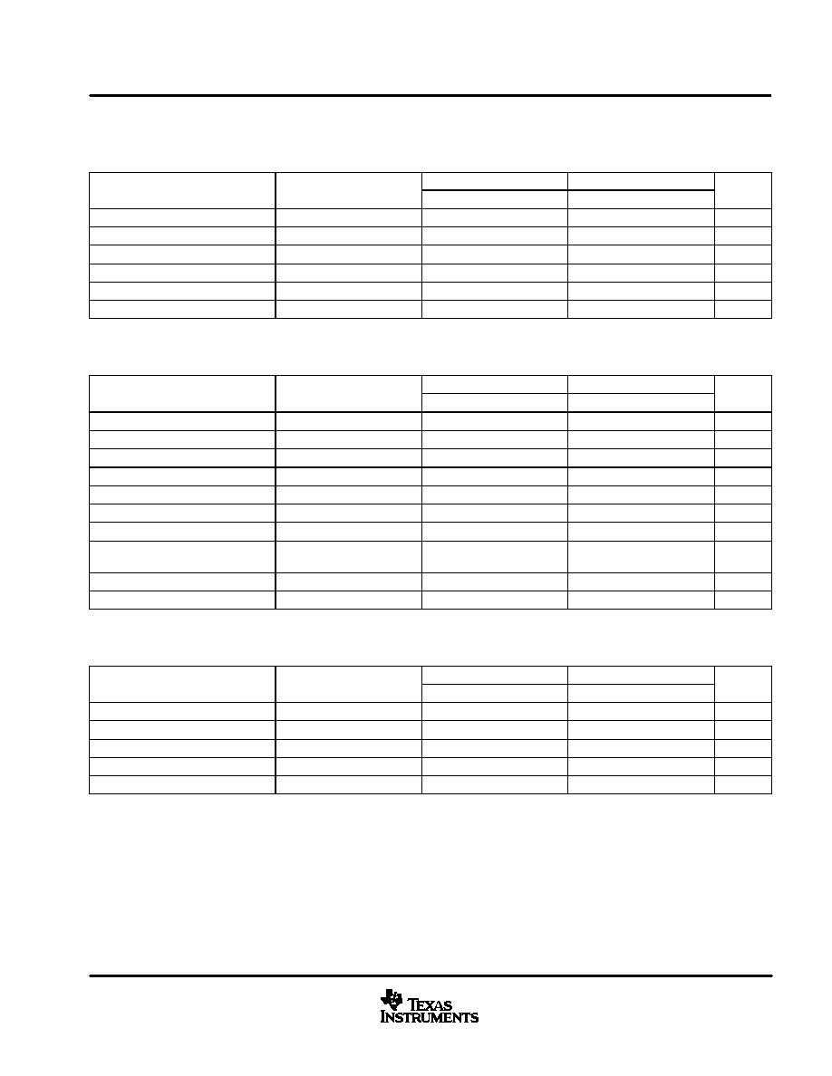
reference
PARAMETER
TEST CONDITIONS
UC2838/UC2838A
UC3838/UC3838A
UNITS
PARAMETER
TEST CONDITIONS
MIN
TYP
MAX
MIN
TYP
MAX
UNITS
Supply current
VCC = VM = 40 V
4
8
4
8
mA
Reference output
TA = 25
∞
C
2.47
2.50
2.53
2.45
2.50
2.55
V
Line regulation
VCC = 5 V to 30 V
1
5
1
10
mV
Load regulation
IO = 0 mA to ≠2 mA
5
20
5
20
mV
Short-circuit current
VREF = 0 V
≠30
≠60
≠30
≠60
mA
Temperature stability
See Note 1
15
25
10
25
mV
NOTE: 1.These parameters are ensured by design but not 100% tested in production.
amplifier (each amplifier)
PARAMETER
TEST CONDITIONS
UC2838/UC2838A
UC3838/UC3838A
UNITS
PARAMETER
TEST CONDITIONS
MIN
TYP
MAX
MIN
TYP
MAX
UNITS
Offset voltage
VCM = 2.5 V
5
10
mV
Input bias current
VIN = 0 V
≠1
≠1
µ
A
Input offset voltage
100
100
nA
Minimum output swing
0.4
18
0.4
18
V
Output sink current
VO = 5 V
1
10
30
1
10
30
mA
Output source current
VO = 0 V
≠1
≠10
≠20
≠1
≠10
≠20
mA
AVOL (open loop gain)
VO = 1 V to 11 V
100
120
100
120
dB
CMRR (common mode rejection ra-
tio)
VIN = 1 V to 11 V
70
80
70
80
dB
PSRR (power supply rejection ratio)
VCC = 10 V to 20 V
70
100
70
100
dB
Gain bandwidth
See Note 1
0.6
0.8
0.6
0.8
MHz
NOTE: 1.These parameters are ensured by design but not 100% tested in production.
reset drive
PARAMETER
TEST CONDITIONS
UC2838/UC2838A
UC3838/UC3838A
UNITS
PARAMETER
TEST CONDITIONS
MIN
TYP
MAX
MIN
TYP
MAX
UNITS
Input leakage
VDR = 40 V
10
10
µ
A
Output leakage
VR = ≠120 V
≠100
≠100
µ
A
Input current
IR = ≠50 mA
≠1
≠2
≠1
≠2
mA
Maximum reset current
IDR = ≠3 mA
≠100
≠120
≠200
≠100
≠120
≠200
mA
Transconductance
IR = ≠10 mA to ≠50 mA
0.03
0.042
0.055
0.03
0.042
0.055
A/V
UC2838, UC2838A
UC3838, UC3838A
SLUS221A ≠ APRIL 2000 ≠ REVISED MAY 2001
4
www.ti.com
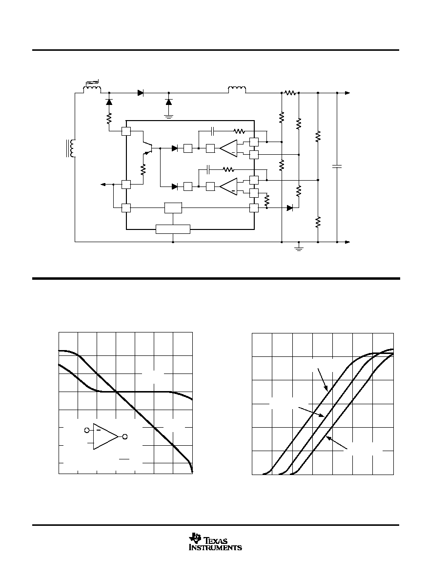
typical application
NOTE: 12 V, 4 A output with switching frequency = 50 kHz.
+
+
3
2
6
7
4.7 k
0.47
8
16
15 k
0.1
1
15
20
14
11
10
REF
9
4, 5, 12, 13
2.5 V
300
1 W
UES1003
UES2403
UES2403
100
0.02
100
9.1 k
1000
3.6 k
12 k
2 k
2.4 k
+
GND
+V O
100
µ
H
UC3838/A
15 V
AUXILLIARY
SUPPLY
12 V
SECONDARY
WINDING
MAGNETIC
AMPLIFIER
45 TURNS
50B10≠1D CORE
APPLICATION INFORMATION
Figure 1.
0.1
10
1 k
10 k
1 M
0
20
40
60
80
100
120
Signal Frequency ≠ Hz
360
315
270
225
180
1.0
100
0.1 M
Phase
Gain
VO
VIN
+
VIN
2.5 V
VO
Gain = 20 Log
140
Gain Magnitude
≠
dB
GAIN MAGNITUDE/PHASE
vs
SIGNAL FREQUENCY
Phase
≠
C
Figure 2.
≠0.2
≠0.4
≠0.8
≠1.0
≠1.2
≠20
≠40
≠60
Input Current ≠ mA
≠80
≠100
0
≠0.6
≠1.4
0
≠120
T J= 25 C
T J= ≠55 C
T J= 125 C
GAIN MAGNITUDE
vs
SIGNAL FREQUENCY
Reset
Current
≠
mA

UC2838, UC2838A
UC3838, UC3838A
SLUS221A ≠ APRIL 2000 ≠ REVISED MAY 2001
5
www.ti.com
APPLICATION INFORMATION
Figure 3.
0
≠20
≠60
≠80
≠100
≠20
≠40
≠60
Reset Voltage ≠ V
≠80
≠100
0
T
J
= 25 C
IB = 0.4 mA
IB = 0.6 mA
IB = 0.8 mA
IB = 1.0 mA
IB = 1.2 mA
≠40
Reset
Current
≠
mA
RESET CURRENT
vs
RESET VOLTAGE
≠120
Figure 4.
Gain Magnitude
≠
dB
GAIN MAGNITUDE/PHASE
vs
SIGNAL FREQUENCY
Phase
≠
C
1 k
10 k
100 k
1 M
10 M
≠30
≠25
≠20
≠15
≠10
≠5
0
5
Signal Frequency ≠ Hz
360
315
270
225
180
GAIN
PHASE
5 V
VO
VIN
GAIN = 20 LOG
IO (dc) = 50 mA
RI = 10
IO (ac) = 10 mA
VO
VIN
Figure 5.
≠1
≠3
≠4
≠5
≠20
≠40
≠60
Input Voltage ≠ V
≠80
≠100
0
≠2
0
≠6
≠120
T J = 25 C
T J = 125 C
VM = 5 V
VIN
IR
Reset
Current
≠
mA
RESET CURRENT
vs
INPUT CURRENT
T J = ≠55 C
Figure 6.
≠50
0
50
100
150
2.45
2.46
2.47
2.48
2.49
2.50
2.51
Junction Temperature ≠
2.52
2.53
2.54
2.55
Reference
V
oltage Output
≠
V
REFERENCE VOLTAGE OUTPUT
vs
JUNCTION TEMPERATURE
∞
C

IMPORTANT NOTICE
Texas Instruments and its subsidiaries (TI) reserve the right to make changes to their products or to discontinue
any product or service without notice, and advise customers to obtain the latest version of relevant information
to verify, before placing orders, that information being relied on is current and complete. All products are sold
subject to the terms and conditions of sale supplied at the time of order acknowledgment, including those
pertaining to warranty, patent infringement, and limitation of liability.
TI warrants performance of its products to the specifications applicable at the time of sale in accordance with
TI's standard warranty. Testing and other quality control techniques are utilized to the extent TI deems necessary
to support this warranty. Specific testing of all parameters of each device is not necessarily performed, except
those mandated by government requirements.
Customers are responsible for their applications using TI components.
In order to minimize risks associated with the customer's applications, adequate design and operating
safeguards must be provided by the customer to minimize inherent or procedural hazards.
TI assumes no liability for applications assistance or customer product design. TI does not warrant or represent
that any license, either express or implied, is granted under any patent right, copyright, mask work right, or other
intellectual property right of TI covering or relating to any combination, machine, or process in which such
products or services might be or are used. TI's publication of information regarding any third party's products
or services does not constitute TI's approval, license, warranty or endorsement thereof.
Reproduction of information in TI data books or data sheets is permissible only if reproduction is without
alteration and is accompanied by all associated warranties, conditions, limitations and notices. Representation
or reproduction of this information with alteration voids all warranties provided for an associated TI product or
service, is an unfair and deceptive business practice, and TI is not responsible nor liable for any such use.
Resale of TI's products or services with
statements different from or beyond the parameters stated by TI for
that product or service voids all express and any implied warranties for the associated TI product or service,
is an unfair and deceptive business practice, and TI is not responsible nor liable for any such use.
Also see: Standard Terms and Conditions of Sale for Semiconductor Products. www.ti.com/sc/docs/stdterms.htm
Mailing Address:
Texas Instruments
Post Office Box 655303
Dallas, Texas 75265
Copyright
2001, Texas Instruments Incorporated