 | –≠–ª–µ–∫—Ç—Ä–æ–Ω–Ω—ã–π –∫–æ–º–ø–æ–Ω–µ–Ω—Ç: UC3852 | –°–∫–∞—á–∞—Ç—å:  PDF PDF  ZIP ZIP |

TYPICAL APPLICATION
10/94
FEATURES
∑
Low-Cost Power Factor
Correction
∑
Power Factor Greater Than 0.99
∑
Few External Parts Required
∑
Controlled On-Time Boost PWM
∑
Zero-Current Switching
∑
Limited Peak Current
∑
Min and Max Frequency Limits
∑
Starting Current Less Than 1mA
∑
High-Current FET Drive Output
∑
Under-Voltage Lockout
DESCRIPTION
The UC1852 provides a low-cost solution to active power-factor correction (PFC)
for systems that would otherwise draw high peak current pulses from AC power
lines. This circuit implements zero-current switched boost conversion, producing
sinusoidal input currents with a minimum of external components, while keeping
peak current substantially below that of fully-discontinuous converters.
The UC1852 provides controlled switch on-time to regulate the output bulk DC
voltage, an off-time defined by the boost inductor, and a zero-current sensing
circuit to reactivate the switch cycle. Even though switching frequency varies with
both load and instantaneous line voltage, it can be maintained within a reasonable
range to minimize noise generation.
While allowing higher peak switch currents than continuous PFCs such as the
UC1854, this device offers less external circuitry and smaller inductors, yet better
performance and easier line-noise filtering than discontinuous current PFCs with
no sacrifice in complexity or cost. The ability to obtain a power factor in excess of
0.99 makes the UC1852 an optimum choice for low-cost applications in the 50 to
500 watt power range. Protection features of these devices include under-voltage
lockout, output clamping, peak-current limiting, and maximum-frequency
clamping.
The UC1852 family is available in 8-pin plastic and ceramic dual in-line packages,
and in the 8-pin small outline IC package (SOIC). The UC1852 is specified for
operation from -55
∞
C to +125
∞
C, the UC2852 is specified for operation from -40
∞
C
to +85
∞
C, and the UC3852 is specified for operation from 0
∞
C to +70
∞
C.
UC1852
UC2852
UC3852
High Power-Factor Preregulator
UDG-92001
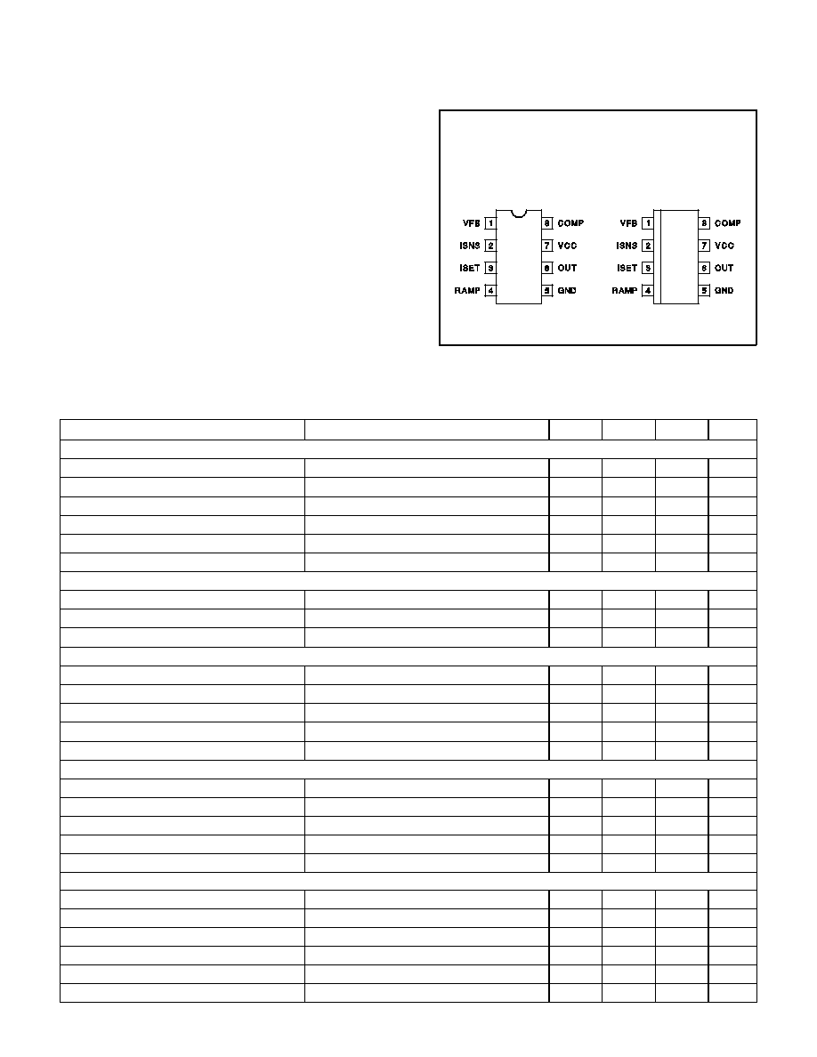
SOIC≠8 (TOP VIEW)
D Package
Unless otherwise stated, VCC=24V, ISET=50k
to GND, RAMP=1nF to GND, ISNS=
≠0.1V, VFB connected to COMP, no load on OUT, ≠55
∞
C<Ta<+125
∞
C for the UC1852,
≠40
∞
C<Ta<+85
∞
C for the UC2852, and 0
∞
C<Ta<+70
∞
C for the UC3852, and Ta=Tj.
UC1852
UC2852
UC3852
ELECTRICAL CHARACTERISTICS
ABSOLUTE MAXIMUM RATINGS
Supply Voltage (Low-impedance Source)..........................30.0V
Supply Current (High-impedance Source) ......................30.0mA
OUT Current, Peak .............................................................
±
1.0A
OUT Energy, Capacitive Load............................................ 5.0
µ
J
Input Voltage, ISNS ............................................................
±
5.0V
Input Voltage, VFB............................................. ≠0.3V to +10.0V
COMP Current ...............................................................
±
10.0mA
ISET Current..................................................................≠10.0mA
Power Dissipation at Ta
25
∞
C (Note 3) ..............................1.0W
Storage Temperature ....................................... ≠65
∞
C to +150
∞
C
Lead Temperature (Soldering, 10 Seconds) ................... +300
∞
C
Note 1: All voltages with respect to GND (Pin 1).
Note 2: All currents are positive into the specified terminal.
Note 3: Refers to DIL-8 Package. Consult Packaging Section of
Unitrode Integrated Circuits databook for thermal limitations and
considerations of package.
DIL≠8 (TOP VIEW)
J or N Package
CONNECTION DIAGRAM
PARAMETER
TEST CONDITIONS
MIN.
TYP.
MAX.
UNITS
Timer Section
ISET Voltage
4.5
5.0
5.5
V
RAMP Charge Current
RAMP=2.5V
88
98
108
µ
A
RAMP Discharge Current
ISNS= ≠1.0V, RAMP=1.0V
12
28
50
mA
RAMP Saturation Voltage
ISNS= ≠1.0V, I
RAMP
=100
µ
A
0.006
0.200
V
RAMP Threshold - Maximum Frequency
VFB=10V, COMP open
0.92
1.02
1.12
V
RAMP Threshold - PWM Comparator
3.9
4.3
4.8
V
Current Sense Comparator
ISNS Restart Threshold
≠18
≠10
≠4
mV
ISNS Fault Threshold
≠550
≠450
≠350
mV
ISNS Input Current
≠100
≠30
100
µ
A
Error Amplifier Section
VFB Input Voltage
4.6
5.0
5.3
V
VFB Input Bias Current
≠5.00
≠0.03
5.00
µ
A
COMP Sink Current
COMP=7.5V
10
mA
COMP Source Current
COMP=2.5V
≠300
≠175
≠100
µ
A
COMP Clamp Voltage
VFB=0.0V, COMP open
9.2
10.0
10.6
V
OUT Output
OUT Saturation Voltage High
VCC=13V, I
OUT
= ≠200mA, RAMP=2V
0.5
1.7
2.5
V
OUT Saturation Voltage Low
I
OUT
=200mA, ISNS= ≠1.0V
0.5
1.6
2.2
V
OUT Saturation Voltage Low @ 10mA
I
OUT
=10mA, ISNS= ≠1.0V
0.05
0.40
V
OUT Clamp Voltage
I
OUT
= ≠200mA, RAMP=2V
10.0
12.0
14.5
V
OUT Voltage during UVLO
I
OUT
=100mA, VCC=0V
0.5
1.0
2.2
V
Overall Section
Inactive Supply Current
VCC=10V
0.2
0.4
1.0
mA
Active Supply Current
3.0
6.0
10.0
mA
VCC Clamp Voltage
ICC=25mA
30
33
36
V
VCC Turn-On Threshold
14.5
16.3
17.5
V
VCC Turn-Off Threshold
10.5
11.5
13.0
V
VCC Threshold Hysteresis
3
5
7
V
UDG-92002
2
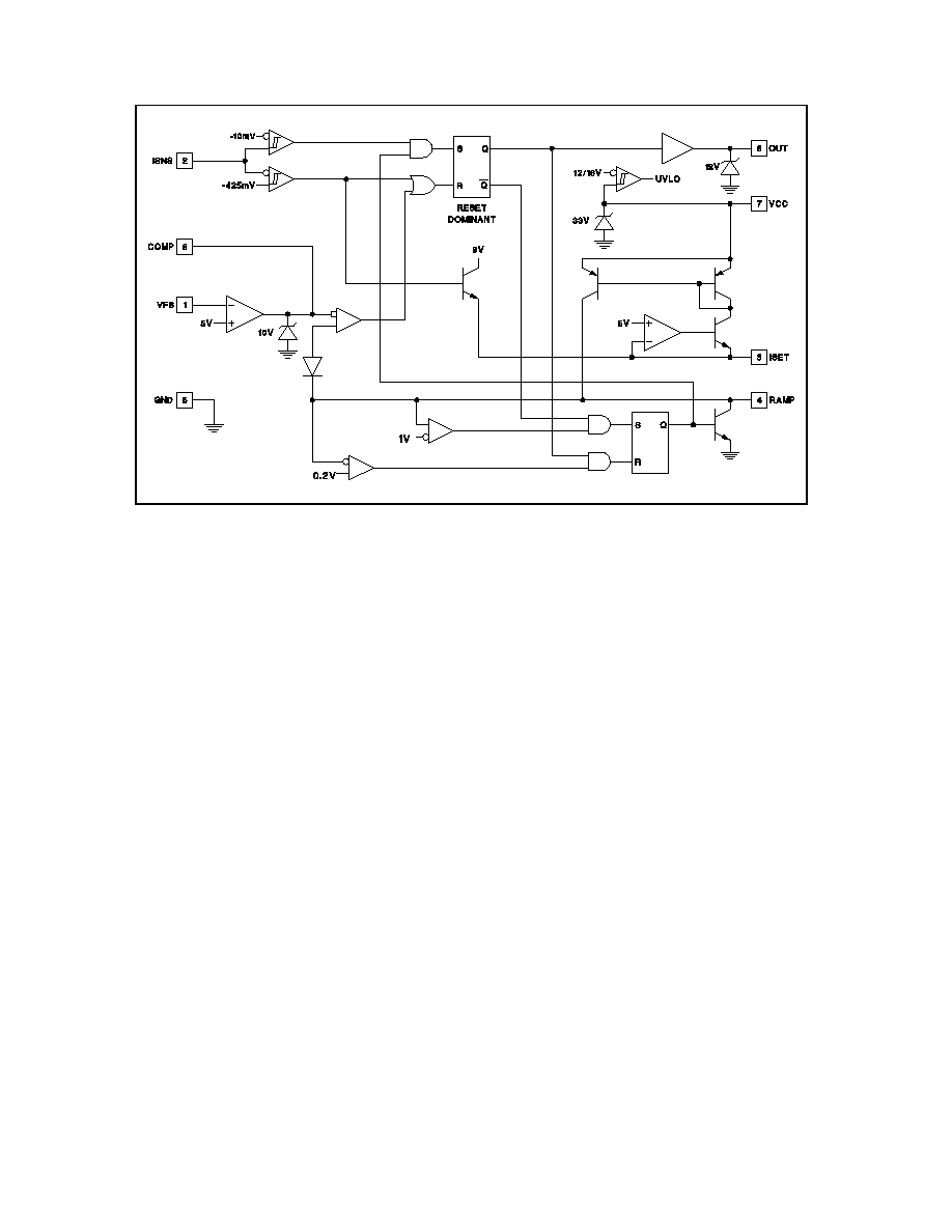
DETAILED BLOCK DIAGRAM
COMP: COMP is the output of the error amplifier and the
input of the PWM comparator. To limit PWM on-time, this
pin is clamped to approximately 10V. To implement soft
start, the COMP pin can be pulled low and ramped up with
a PNP transistor, a capacitor, and a resistor.
GND: Ground for all functions is through this pin.
ISET: The dominant function is of this pin is to program
RAMP charging current. RAMP charging current is
approximately 5V divided by the external resistor placed
from ISET to ground. Resistors in the range of 10k
to
50k
are recommended, producing currents in the range
of 100
µ
A to 500
µ
A.
A second function of ISET is as reference output. The ISET
pin is normally regulated to 5V
±
10%. It is critical that this
pin only see the loading of the RAMP programming resistor,
but a high input-impedance comparator or amplifier may be
connected to this pin or to a tap on the RAMP programming
resistor if required.
The third function of the ISET pin is as a FAULT output. In
the event of an over-current fault, the ISET pin is forced to
approximately 9V by the fault comparator. This can be used
to trip an external protection circuit which can disable the
load or start a fault restart cycle.
ISNS: This input to the zero and over current comparators
is specially built to allow operation over a
±
5V dynamic
range. In noisy systems or systems with very high Q
inductors, it is desirable to filter the signal entering the ISNS
input to prevent premature restart or fault cycles. For best
accuracy, ISNS should be connected to a current sense
resistor through no more than 200 ohms.
OUT: The output of a high-current power driver capable of
driving the gate of a power MOSFET with peak currents
exceeding
±
500mA. To prevent damage to the power
MOSFET, the OUT pin is internally driven by a 12V supply.
However, lead inductance between the OUT pin and the
load can cause overshoot and ringing. External current
boost transistors will increase this overshoot and ringing. If
there is any significant distance between the IC and the
MOSFET, external clamp diodes and/or series damping
resistors may be required. OUT is actively held low when
the VCC is below the UVLO threshold.
RAMP: A controlled on-time PWM requires a timer whose
time can be modulated by an external voltage. The timer
current is programmed by a resistor from ISET to GND. A
capacitor from RAMP to GND sets the on time in
conjunction with the voltage on COMP. Recommended
values for the timer capacitors are between 100pF and 1nF.
VCC: VCC is the logic and control power connection for this
device. VCC current is the sum of active device supply
current and the average OUT current. Knowing the
maximum operating frequency and the MOSFET gate
charge (Qg), average OUT current can be estimated by:
I
OUT
=
Q
g
◊
F
To prevent noise problems, bypass VCC to GND with both
a ceramic and an electrolytic capacitor.
VFB: VFB is the error amplifier inverting input. This input
serves as both the voltage sense input to the error amplifier
UC1852
UC2852
UC3852
PIN DESCRIPTIONS
UDG-92003
3
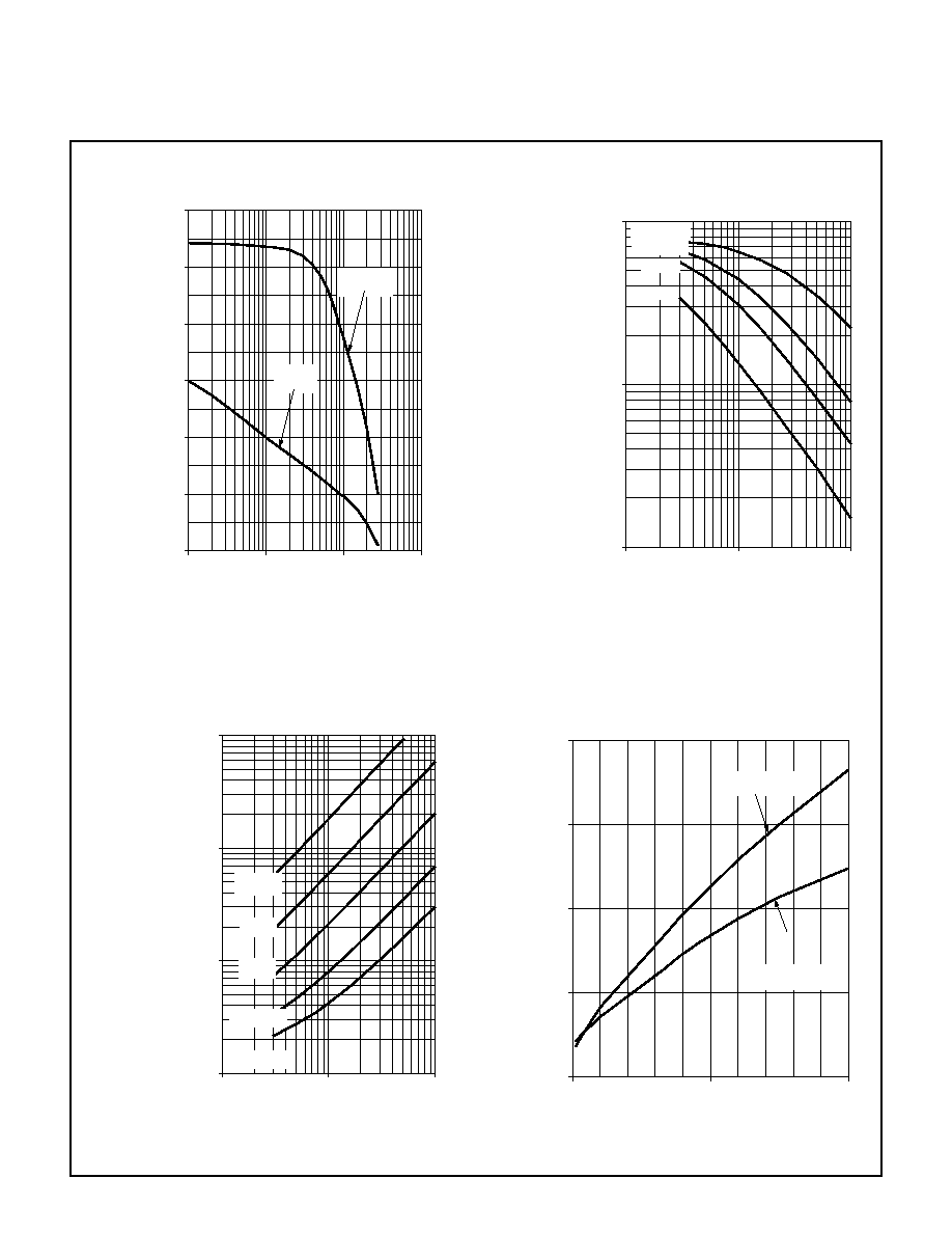
Max Frequency vs. Rset and Ct
Rset, k
Maximum
Frequency,
kHz
10
100
1000
1
10
100
100pF
500pF
1nF
3nF
OUT Rise and Fall Time
Load Capacitance, nF
ns
0
50
100
150
200
0
5
10
Rise Time
Fall Time
Error Amplifier Gain and Phase
Frequency, kHz
Gain
(dB)
Phase
(deg)
-20
0
20
40
60
80
100
10
100
1000
10000
Phase
Gain
Max On-Time vs. Rset and Ct
Rset, k
Maximum
On-Time
µ
s
1
10
100
1000
1
10
100
100pF
300pF
1nF
3nF
10nF
UC1852
UC2852
UC3852
UDG-92006
UDG-92008
UDG-92005
TYPICAL CHARACTERISTICS
UDG-92007
4
UNITRODE INTEGRATED CIRCUITS
7 CONTINENTAL BLVD.
∑
MERRIMACK, NH 03054
TEL. (603) 424-2410
∑
FAX (603) 424-3460
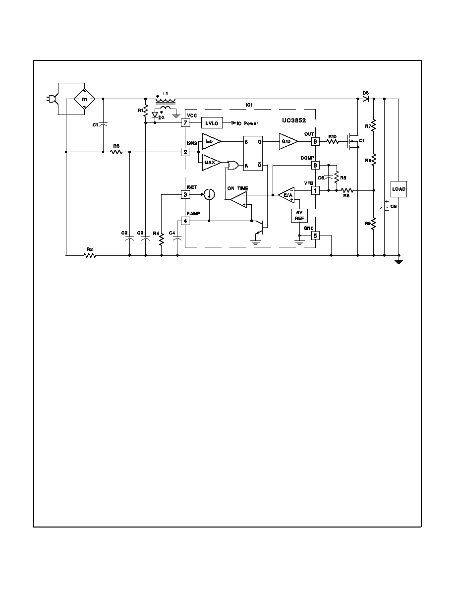
APPLICATION INFORMATION: A 100 Watt Power Factor Preregulator
This circuit demonstrates a complete power factor preregulator based on the UC3852. This preregulator will supply
up to 100 watts at 400VDC and exhibit power factor greater than 0.995 with less than 10% total harmonic distortion.
Operating input range is 90V to 160V RMS at 50Hz to 60Hz.
This design is intentionally simple, yet fully functional. The UC3852 can also be used in designs featuring soft start,
over-voltage protection, wide power-line voltage operation, and fault latching. For more information on applying
the UC3852, refer to Unitrode Application Note U≠132.
PARTS LIST
UC1852
UC2852
UC3852
UDG-92004
C1
0.47
µ
F/250VAC X2 Class Polyester
C2
1nF/16V Ceramic
C3
68
µ
F/35V Aluminum Electrolytic
C4
180pF/16V Ceramic
C5
0.1
µ
F/16V Polyester or Ceramic
C6
82
µ
F/450V Aluminum Electrolytic
D1
2A/500V Bridge Rectifier (Collmer
KBPC106 or Powertex MB11A02V60)
D2
100mA/50V Switching Diode (1N4148)
D3
2A/500V 250ns Recovery-Time Rectifier
(Motorola MR856)
IC1
UC3852N Power Factor Controller IC
Q1
IRF830 4.5A/500V 1.5
Power FET
L1
680
µ
H (Renco RL3792 with
10 Turn 24 AWG Secondary)
R1
150k
,
1
/
4
W
R2
0.2
,
1
/
2
W Carbon Composition
R3
10
,
1
/
4
W
R4
13.3k
,
1
/
4
W
R5
1M
,
1
/
4
W
R6
20k
,
1
/
4
W
R7
200k
,
1
/
2
W
R8
200k
,
1
/
2
W
5

IMPORTANT NOTICE
Texas Instruments and its subsidiaries (TI) reserve the right to make changes to their products or to discontinue
any product or service without notice, and advise customers to obtain the latest version of relevant information
to verify, before placing orders, that information being relied on is current and complete. All products are sold
subject to the terms and conditions of sale supplied at the time of order acknowledgement, including those
pertaining to warranty, patent infringement, and limitation of liability.
TI warrants performance of its semiconductor products to the specifications applicable at the time of sale in
accordance with TI's standard warranty. Testing and other quality control techniques are utilized to the extent
TI deems necessary to support this warranty. Specific testing of all parameters of each device is not necessarily
performed, except those mandated by government requirements.
CERTAIN APPLICATIONS USING SEMICONDUCTOR PRODUCTS MAY INVOLVE POTENTIAL RISKS OF
DEATH, PERSONAL INJURY, OR SEVERE PROPERTY OR ENVIRONMENTAL DAMAGE ("CRITICAL
APPLICATIONS"). TI SEMICONDUCTOR PRODUCTS ARE NOT DESIGNED, AUTHORIZED, OR
WARRANTED TO BE SUITABLE FOR USE IN LIFE-SUPPORT DEVICES OR SYSTEMS OR OTHER
CRITICAL APPLICATIONS. INCLUSION OF TI PRODUCTS IN SUCH APPLICATIONS IS UNDERSTOOD TO
BE FULLY AT THE CUSTOMER'S RISK.
In order to minimize risks associated with the customer's applications, adequate design and operating
safeguards must be provided by the customer to minimize inherent or procedural hazards.
TI assumes no liability for applications assistance or customer product design. TI does not warrant or represent
that any license, either express or implied, is granted under any patent right, copyright, mask work right, or other
intellectual property right of TI covering or relating to any combination, machine, or process in which such
semiconductor products or services might be or are used. TI's publication of information regarding any third
party's products or services does not constitute TI's approval, warranty or endorsement thereof.
Copyright
©
1999, Texas Instruments Incorporated