 | –≠–ª–µ–∫—Ç—Ä–æ–Ω–Ω—ã–π –∫–æ–º–ø–æ–Ω–µ–Ω—Ç: UC3856QTR | –°–∫–∞—á–∞—Ç—å:  PDF PDF  ZIP ZIP |

Improved Current Mode PWM Controller
UC1856
UC2856
UC3856
DESCRIPTION
FEATURES
∑
Pin-for-Pin Compatible With the UC3846
∑
65ns Typical Delay From Shutdown to
Outputs, and 50ns Typical Delay From
Sync to Outputs
∑
Improved Current Sense Amplifier With
Reduced Noise Sensitivity
∑
Differential Current Sense with 3V
Common Mode Range
∑
Trimmed Oscillator Discharge Current
for Accurate Deadband Control
∑
Accurate 1V Shutdown Threshold
∑
High Current Dual Totem Pole Outputs
(1.5A peak)
∑
TTL Compatible Oscillator SYNC Pin
Thresholds
∑
4kV ESD Protection
The UC3856 is a high performance version of the popular UC3846
series of current mode controllers, and is intended for both design
upgrades and new applications where speed and accuracy are impor-
tant. All input to output delays have been minimized, and the current
sense output is slew rate limited to reduce noise sensitivity. Fast 1.5A
peak output stages have been added to allow rapid switching of
power FETs.
A low impedance TTL compatible sync output has been implemented
with a tri-state function when used as a sync input.
Internal chip grounding has been improved to minimize internal
"noise" caused when driving large capacitive loads. This, in conjunc-
tion with the improved differential current sense amplifier results in
enhanced noise immunity.
Other features include a trimmed oscillator current (8%) for accurate
frequency and dead time control; a 1V, 5% shutdown threshold; and
4kV minimum ESD protection on all pins.
BLOCK DIAGRAM
9/96
UDG-96176
2
UC1856
UC2856
UC3856
ABSOLUTE MAXIMUM RATINGS
Supply Voltage ....................................................................
+
40V
Collector Supply Voltage .....................................................
+
40V
Output Current, Source or Sink
DC...................................................................................0.5A
Pulse (0.5
µ
s)...................................................................2.0A
Error Amp Inputs....................................................
-
0.3V to
+
V
IN
Shutdown Input.....................................................
-
0.3V to
+
10V
Current Sense Inputs..............................................
-
0.3V to
+
3V
SYNC Output Current ......................................................±10mA
Error Amplifier Output Current ...........................................
-
5mA
Soft Start Sink Current.......................................................50mA
Oscillator Charging Current .................................................5mA
Power Dissipation at T
A
=
25
∞
C (Note 2).......................1000mW
Power Dissipation at T
C
=
25
∞
C (Note 2) ......................2000mW
Junction Temperature .......................................
-
55
∞
C to
+
150
∞
C
Storage Temperature Range ............................
-
65
∞
C to
+
150
∞
C
Lead Temperature (Soldering, 10 sec.) ...........................
+
300
∞
C
All voltages are with respect to Ground. Currents are positive
into, negative out of the specified terminal. Consult packaging
section of databook for thermal limitations and considerations of
package.
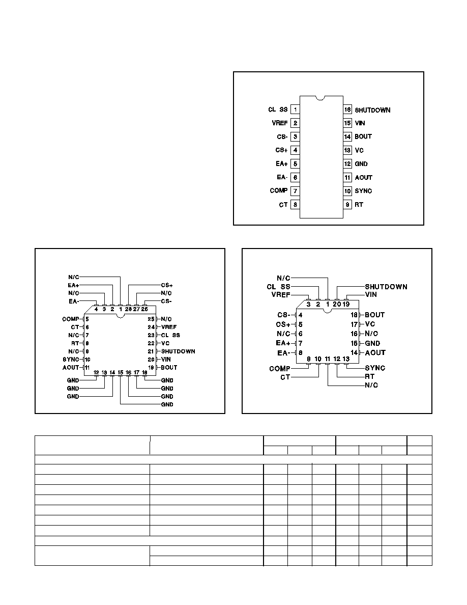
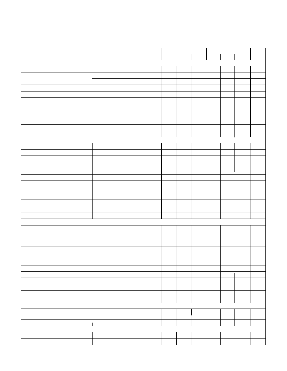
CONNECTION DIAGRAMS
DIL≠16, SOIC-16 (Top View)
J or N, DW PACKAGE
PLCC-20 (Top View)
Q PACKAGE
PLCC-28 (Top View)
QP PACKAGE
ELECTRICAL CHARACTERISTICS
Unless otherwise stated, these specifications apply for T
A
=
-
55
∞
C to +125
∞
C for
UC1856;
-
40
∞
C to +85
∞
C for the UC2856; and 0
∞
C to +70
∞
C for the UC3856, VIN
=
15V, RT
=
10k, CT
=
1nF, T
A
=
T
J
.
UC1856/UC2856
UC3856
PARAMETER
TEST CONDITIONS
MIN
TYP
MAX
MIN
TYP
MAX
UNITS
Reference Section
Output Voltage
T
J
=
25∞C, Io
=
1mA
5.05
5.10
5.15
5.00
5.10
5.20
V
Line Regulation
VIN
=
8V to 40V
20
20
mV
Load Regulation
Io
= -
1mA to
-
10mA
15
15
mV
Total Output Variation
Line, Load, and Temperature
5.00
5.20
4.95
5.25
V
Output Noise Voltage
10Hz < f < 10kHz, T
J
=
25∞C
50
50
µ
V
Long Term Stability
T
J
=
125∞C, 1000 Hrs (Note 2)
5
25
5
25
mV
Short Circuit Current
VREF
=
0V
-
25
-
45
-
65
-
25
-
45
-
65
mA
Oscillator Section
Initial Accuracy
T
J
=
25∞C
180
200
220
180
200
220
kHz
Over Operating Range
170
230
170
230
kHz
3
UC1856
UC2856
UC3856
ELECTRICAL CHARACTERISTICS (cont.)
Unless otherwise stated, these specifications apply for T
A
=
-
55
∞
C to
+125
∞
C for UC1856;
-
40
∞
C to +85
∞
C for the UC2856; and 0
∞
C to +70
∞
C for the UC3856, VIN
=
15V, RT
=
10k, CT
=
1nF, T
A
=
T
J
.
UC1856/UC2856
UC3856
PARAMETER
TEST CONDITIONS
MIN
TYP
MAX
MIN
TYP
MAX
UNITS
Oscillator Section (cont.)
Voltage Stability
VIN
=
8V to 40V
2
2
%
Discharge Current
T
J
=
25∞C, V
CT
=
2V
7.5
8.0
8.8
7.5
8.0
8.8
mA
V
CT
=
2V
6.7
8.0
8.8
6.7
8.0
8.8
mA
Sync Output High Level
Io
= -
1mA
2.4
3.6
2.4
3.6
V
Sync Output Low Level
Io
= +
1mA
0.2
0.4
0.2
0.4
V
Sync Input High Level
CT
=
0V, RT
=
VREF
2.0
1.5
2.0
1.5
V
Sync Input Low Level
CT
=
0V, RT
=
VREF
1.5
0.8
1.5
0.8
V
Sync Input Current
CT
=
0V, RT
=
VREF
1
10
1
10
µ
A
V
SYNC
=
5V
Sync Delay to Outputs
CT
=
0V, RT
=
VREF
50
100
50
100
ns
V
SYNC
=
0.8V to 2V
Error Amplifier Section
Input Offset Voltage
V
CM
=
2V
5
10
mV
Input Bias Current
-
1
-
1
µ
A
Input Offset Current
500
500
nA
Common Mode Range
VIN
=
8V to 40V
0
VIN
-
2
0
VIN
-
2
V
Open Loop Gain
Vo
=
1.2V to 3V
80
100
80
100
dB
Unity Gain Bandwidth
T
J
=
25∞C
1
1.5
1
1.5
MHz
CMRR
V
CM
=
0V to 38V, VIN = 40V
75
100
75
100
dB
PSRR
VIN
=
8V to 40V
80
100
80
100
dB
Output Sink Current
V
ID
= -
15mV, Vc
OMP
= 1.2V
5
10
5
10
mA
Output Source Current
V
ID
=
15mV, V
COMP
=
2.5V
-
0.4
-
0.5
-
0.4
-
0.5
mA
Output High Level
V
ID
=
50mV, R
L
(COMP)
=
15k
4.3
4.6
4.9
4.3
4.6
4.9
V
Output Low Level
V
ID
= -
50mV, R
L
(COMP)
=
15k
0.7
1
0.7
1
V
Current Sense Amplifier Section
Amplifier Gain
V
CS
- =
0V, CL SS Open (Notes 3,4)
2.5
2.75
3.0
2.5
2.75
3.0
V/V
Maximum Differential
CL SS Open (Note 3)
1.1
1.2
1.1
1.2
V
Input Signal (V
CS
+
-
Vcs-)
R
L
(COMP)
=
15k
Input Offset Voltage
V
CL SS
=
0.5V
5
35
5
35
mV
COMP Open (Note 3)
CMRR
V
CM
=
0V to 3V
60
60
dB
PSRR
VIN
=
8V to 40V
60
60
dB
Input Bias Current
V
CL SS
=
0.5V, COMP Open (Note 3)
-
1
-
3
-
1
-
3
µ
A
Input Offset Current
V
CL SS
=
0.5V, COMP Open (Note 3)
1
1
mA
Input Common Mode Range
0
3
0
3
V
Delay to Outputs
V
EA
+
=
VREF, EA
- =
0V
120
250
120
250
ns
CS+
-
CS
- =
0V to 1.5V
Current Limit Adjust Section
Current Limit Offset
V
CS
- = 0V
0.43
0.5
0.57
0.43
0.5
0.57
V
V
CS
+ = 0V, COMP = Open (Note 3)
Input Bias Current
V
EA
+
=
VREF, V
EA
- =
0V
-
10
-
30
-
10
-
30
µ
A
Shutdown Terminal Section
Threshold Voltage
0.95
1.00
1.05
0.95
1.00
1.05
V
Input Voltage Range
0
5
0
5
V
4
Note 1: All voltages are with respect to GND. Currents are positive into, negative out of the specified terminal.
Note 2: This parameter, although guaranteed over the recommended operating conditions is not 100% tested in production.
Note 3: Parameter measured at trip point of latch with V
EA
+ = VREF, V
EA
- =
0V.
Note 4: Amplifier gain defined as:
V
COMP
G
=
;
V
CS
- =
0V to 1.0V
V
CS
+
Note 5: Current into CL SS guaranteed to latch circuit into shutdown state.
Note 6: Current into CL SS guaranteed not to latch circuit into shutdown state.
UC1856
UC2856
UC3856
UC1856/UC2856
UC3856
PARAMETER
TEST CONDITIONS
MIN
TYP
MAX
MIN
TYP
MAX
UNITS
Shutdown Terminal Section (cont.)
Minimum Latching
(Note 5)
3
1.5
3
1.5
mA
Current (I
CL SS
)
Maximum Non-Latching
(Note 6)
1.5
0.8
1.5
0.8
mA
Current (I
CL SS
)
Delay to Outputs
V
SHUTDOWN
=
0 to 1.3V
65
110
65
110
ns
Output Section
Collector-Emitter Voltage
40
40
V
Off-State Bias Current
VC
=
40V 250
250
µ
A
Output Low Level
I
OUT
=
20mA
0.1
0.5
0.1
0.5
V
I
OUT
=
200mA
0.5
2.6
0.5
2.6
V
Output High Level
I
OUT
= -
20mA
12.5
13.2
12.5
13.2
V
I
OUT
= -
200mA
12
13.1
12
13.1
V
Rise Time
C1
=
1nF
40
80
40
80
ns
Fall Time
C1
=
1nF
40
80
40
80
ns
UVLO Low Saturation
VIN
=
0V, I
OUT
=
20mA
0.8
1.5
0.8
1.5
V
PWM Section
Maximum Duty Cycle
45
47
50
45
47
50
%
Minimum Duty Cycle
0
0
%
Undervoltage Lockout Section
Startup Threshold
7.7
8.0
7.7
8.0
V
Threshold Hysterisis
0.7
0.7
V
Total Standby Current
Supply Current
18
23
18
23
mA
ELECTRICAL CHARACTERISTICS (cont.)
Unless otherwise stated, these specifications apply for T
A
=
-
55
∞
C to
+125
∞
C for UC1856;
-
40
∞
C to +85
∞
C for the UC2856; and 0
∞
C to +70
∞
C for the UC3856, VIN
=
15V, RT
=
10k, CT
=
1nF, T
A
=
T
J
.
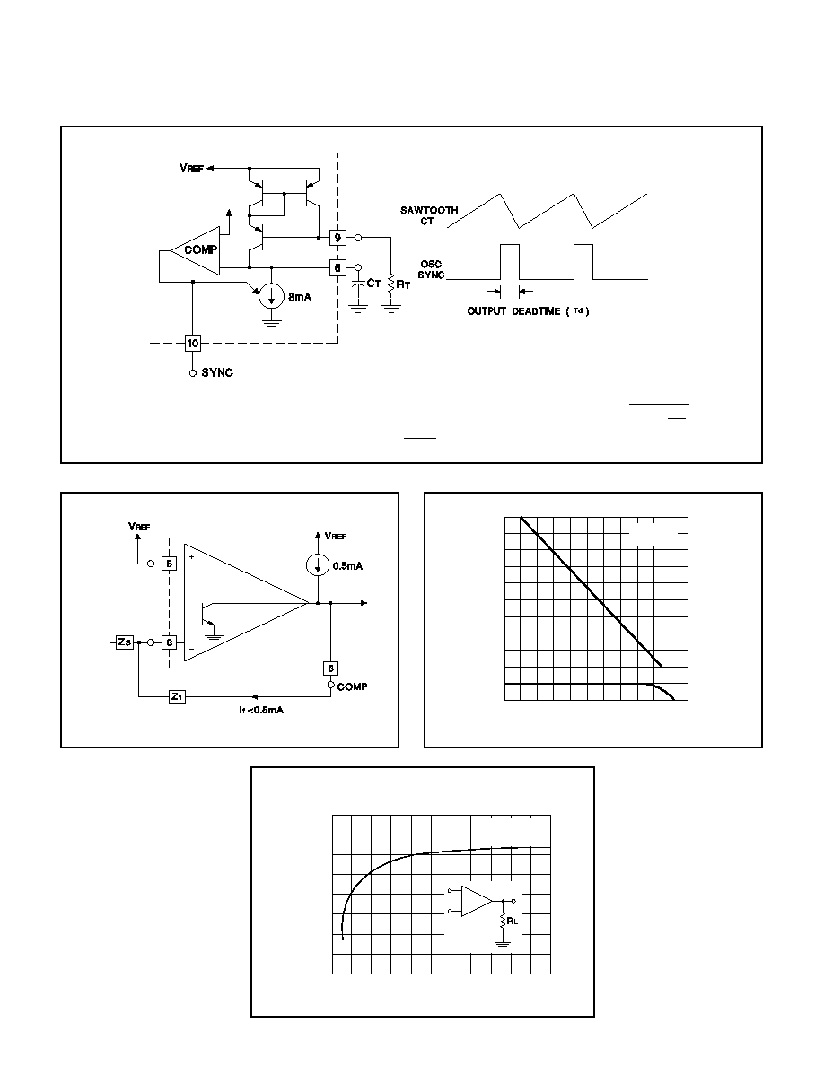
5
OPEN-LOOP
VOL
T
AGE GAIN (dB)
OUTPUT LOAD RESISTANCE R
L
(k-OHMS)
0
70
80
90
100
110
V
IN
=20V
T
J
=
25
o
10 20 30
40 50 60 70
80 90 100
OPEN-LOOP
VOL
T
AGE GAIN (dB)
FREQUENCY (Hz)
100
1k
10k
100k
1M
0
20
40
60
80
OPEN-LOOP
PHASE
V
IN
=20V
T
J
=25
o
-180
o
-90
o
0
o
APPLICATIONS INFORMATION
Error Amplifier Output Configuration
Error Amplifier Gain and Phase vs Frequency
Error Amplifier Open-Loop D.C. Gain vs
Load Resistance
UC1856
UC2856
UC3856
Error Amplifier can source up to 0.5mA.
UDG-96178
UDG-96179
UDG-96180
Oscillator Circuit
Output deadtime is determined by size of the external capacitor, C
T
, according to the formula: Td
=
For large values of R
T
: Td
=
250C
T
Oscillator frequency is approximated by the formula: f
T
=
2C
T
8mA
-
........
3.6
R
T
2
R
T
C
T
UDG-96177
6
UC1856
UC2856
UC3856
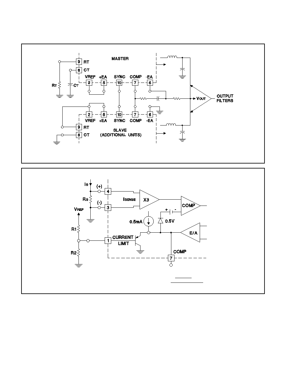
Parallel Operation
Slaving allows parallel operation of two or more units with equal current sharing.
Peak current (I
S
) is determined by the formula: I
S
=
( )
-
0.5
R2 V
REF
R1 + R2
3R
S
UDG-96181
UDG-96182
APPLICATIONS INFORMATION (cont.)
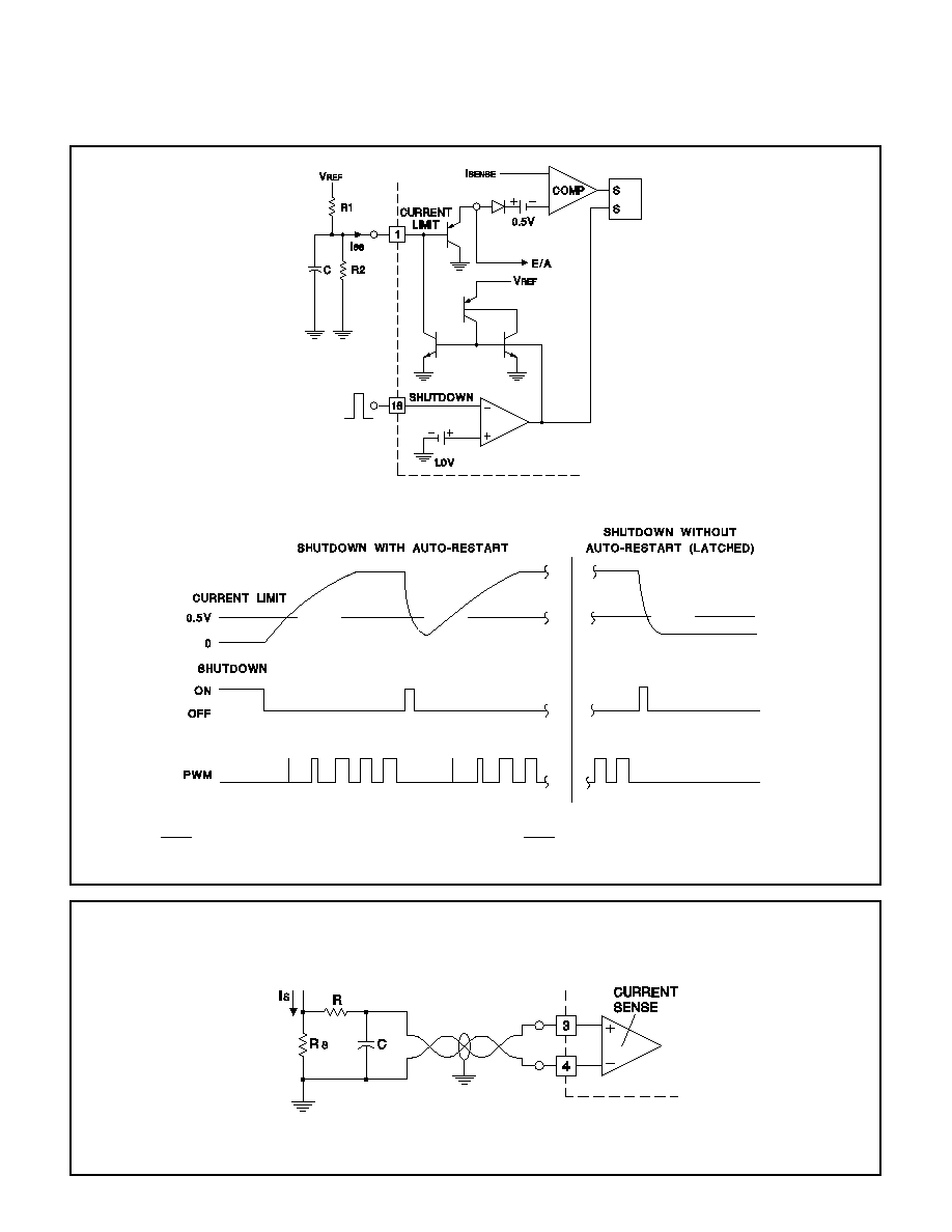
Pulse by Pulse Current Limiting
7
UC1856
UC2856
UC3856
V
REF
R1
If
<
0.8mA, the shutdown latch will commutate
when I
SS
=
0.8mA and a restart cycle will be initiated.
V
REF
R1
If
>
3mA, the device will latch off until power is
recycled.
APPLICATIONS DATA (cont.)
UDG-96183
UDG-96184
Current Sense Amplifier Connections
A small RC filter may be required in some applications to reduce switch transients.
Differential input allows remote, noise sensing.
UDG-96185
8
UC1856
UC2856
UC3856
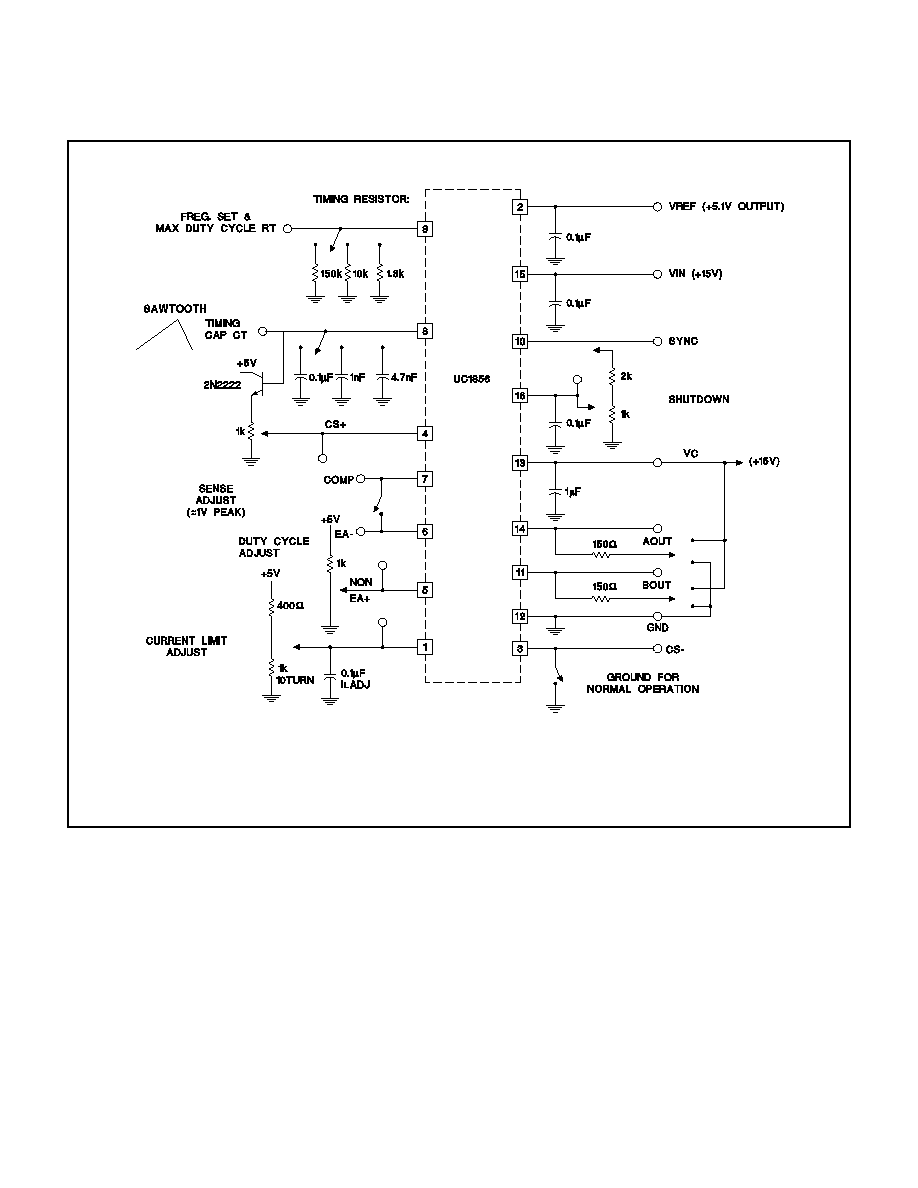
UC1856 Open Loop Test Circuit
UNITRODE INTEGRATED CIRCUITS
7 CONTINENTAL BLVD. ∑ MERRIMACK, NH 03054
TEL. 603-424-2410 ∑ FAX 603-424-3460
- BYPASS CAPS SHOULD BE LOW ESR & ESL TYPE
- SHORT E/A- & COMP FOR UNITY GAIN TESTING
THE USE OF A GROUND PLANE IS HIGHLY RECOMMENDED
APPLICATIONS INFORMATION (cont.)
UDG-96186

IMPORTANT NOTICE
Texas Instruments and its subsidiaries (TI) reserve the right to make changes to their products or to discontinue
any product or service without notice, and advise customers to obtain the latest version of relevant information
to verify, before placing orders, that information being relied on is current and complete. All products are sold
subject to the terms and conditions of sale supplied at the time of order acknowledgement, including those
pertaining to warranty, patent infringement, and limitation of liability.
TI warrants performance of its semiconductor products to the specifications applicable at the time of sale in
accordance with TI's standard warranty. Testing and other quality control techniques are utilized to the extent
TI deems necessary to support this warranty. Specific testing of all parameters of each device is not necessarily
performed, except those mandated by government requirements.
CERTAIN APPLICATIONS USING SEMICONDUCTOR PRODUCTS MAY INVOLVE POTENTIAL RISKS OF
DEATH, PERSONAL INJURY, OR SEVERE PROPERTY OR ENVIRONMENTAL DAMAGE ("CRITICAL
APPLICATIONS"). TI SEMICONDUCTOR PRODUCTS ARE NOT DESIGNED, AUTHORIZED, OR
WARRANTED TO BE SUITABLE FOR USE IN LIFE-SUPPORT DEVICES OR SYSTEMS OR OTHER
CRITICAL APPLICATIONS. INCLUSION OF TI PRODUCTS IN SUCH APPLICATIONS IS UNDERSTOOD TO
BE FULLY AT THE CUSTOMER'S RISK.
In order to minimize risks associated with the customer's applications, adequate design and operating
safeguards must be provided by the customer to minimize inherent or procedural hazards.
TI assumes no liability for applications assistance or customer product design. TI does not warrant or represent
that any license, either express or implied, is granted under any patent right, copyright, mask work right, or other
intellectual property right of TI covering or relating to any combination, machine, or process in which such
semiconductor products or services might be or are used. TI's publication of information regarding any third
party's products or services does not constitute TI's approval, warranty or endorsement thereof.
Copyright
©
1999, Texas Instruments Incorporated