UC1860
UC2860
UC3860
Resonant Mode Power Supply Controller
FEATURES
∑
3MHz VFO Linear over 100:1 Range
∑
5MHz Error Amplifier with Controlled
Output Swing
∑
Programmable One Shot Timer--
Down to 100ns
∑
Precision 5V Reference
∑
Dual 2A Peak Totem Pole Outputs
∑
Programmable Output Sequence
∑
Programmable Under Voltage Lockout
∑
Very Low Start Up Current
∑
Programmable Fault Management &
Restart Delay
∑
Uncommitted Comparator
DESCRIPTION
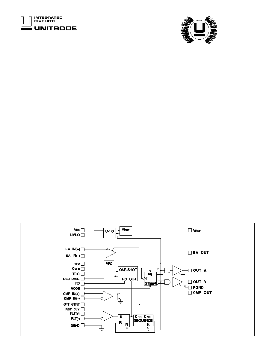
The UC1860 family of control ICs is a versatile system for resonant mode
power supply control. This device easily implements frequency modulated
fixed-on-time control schemes as well as a number of other power supply
control schemes with its various dedicated and programmable features.
The UC1860 includes a precision voltage reference, a wide-bandwidth er-
ror amplifier, a variable frequency oscillator operable to beyond 3MHz, an
oscillator-triggered one-shot, dual high-current totem-pole output drivers,
and a programmable toggle flip-flop. The output mode is easily pro-
grammed for various sequences such as A, off, B, off; A & B, off; or A, B,
off. The error amplifier contains precision output clamps that allow pro-
gramming of minimum and maximum frequency.
The device also contains an uncommitted comparator, a fast comparator
for fault sensing, programmable soft start circuitry, and a programmable
restart delay. Hic-up style response to faults is easily achieved. In addi-
tion, the UC1860 contains programmable under voltage lockout circuitry
that forces the output stages low and minimizes supply current during
start-up conditions.
BLOCK DIAGRAM
ABSOLUTE MAXIMUM RATINGS
Supply Voltage (pin 19) . . . . . . . . . . . . . . . . . . . . . . . . . . . . 20V
Output Current, Source or Sink (pins 17 & 20)
DC . . . . . . . . . . . . . . . . . . . . . . . . . . . . . . . . . . . . . . . . . . 0.8A
Pulse (0.5
µ
s) . . . . . . . . . . . . . . . . . . . . . . . . . . . . . . . . . . 3.0A
Power Ground Voltage . . . . . . . . . . . . . . . . . . . . . . . . . . . .
±
0.2V
Inputs (pins 1, 2, 3, 4, 8, 9, 11, 12,
13, 14, 21, 22, 23 & 24) . . . . . . . . . . . . . . . . . . . . . . -0.4 to 6V
Error Amp Output Current, Source or Sink (pin 5) . . . . . . . . 2mA
I
VFO
Current (pin 7). . . . . . . . . . . . . . . . . . . . . . . . . . . . . . . . 2mA
Comparator Output Current (pin 15) . . . . . . . . . . . . . . . . . . 5mA
Comparator Output Voltage (pin 15) . . . . . . . . . . . . . . . . . . 15V
Soft Start or Restart Delay Sink Current (pins 22 & 23) . . . 5mA
Power Dissipation at T
A
= 50∞C (DIP) . . . . . . . . . . . . . . . 1.25W
Power Dissipation at T
A
= 50
∞
C (PLCC) . . . . . . . . . . . . . . . . 1W
Lead Temperature (Soldering, 10 seconds) . . . . . . . . . . . 300∞C
Note: All voltages are with respect to signal ground and all
currents are positive into the specified terminal.
Pin numbers refer to the DIP.
Refer to Packaging Section of Databook for thermal
limitations and considerations of packages.
10/93
UC1860
UC2860
UC3860
ELECTRICAL CHARACTERISTICS:
PARAMETER
CONDITIONS
MIN
TYP
MAX
UNITS
Reference Section
Output Voltage
T
A
= 25∞C, I
O
= 0
4.95
5.00
5.05
V
I
O
= 0, Over Temp
4.93
5.07
V
Line Regulation
10
V
CC
20V
2
15
mV
Load Regulation
0
I
O
10mA
2
25
mV
Output Noise Voltage*
10Hz
f
10kHz
50
µ
V
RMS
Short Circuit Current
V
REF
= 0V
-150
-15
mA
Error Amplifier Section
Input Offset Voltage
2.8
V
CM
4.5V
1
8
mV
Input Bias Current
50
500
nA
Open Loop Gain
dV
O
= 1.5V
60
80
dB
PSRR
10
V
CC
20V
70
100
dB
Output Low (V
O
-VI
VFO
)
-0.1
I
O
0.1mA
-8
0
8
mV
Output High (V
O
-VI
VFO
)
-0.5
I
O
0.5mA
1.9
2
2.1
V
Unity Gain Bandwidth*
R
IN
= 2k
4
5
MHz
Oscillator Section
Nominal Frequency*
1.0
1.5
2.0
MHz
dF/dI
OSC
*
100
I
VFO
500
µ
A
2
3
4
GHz/A
*Guaranteed by design but not 100% tested.
Unless otherwise stated, all specifications apply for -55∞C
T
A
125∞C for the
UC1860, -25∞C
T
A
85∞C for the UC2860, 0
T
A
70∞C for the UC3860, V
CC
=
12V, C
VFO
= 330pF, I
VFO
= 0.5mA, C = 330pF, and R = 2.7k, T
A
= T
J.
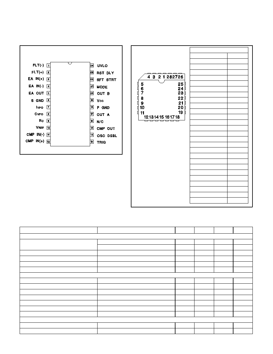
DIL - 24 (TOP VIEW)
J or N Package
PLCC-28, LCC-28
(TOP VIEW)
Q or L Package
PIN PACKAGE FUNCTION
FUNCTION
PIN
S GND
1
I
VFO
2
C
VFO
3
RC
4
V
REF
5
CMP IN (-)
6
CMP IN (+)
7
TRIG
8
OSC DSBL
9
CMP OUT
10
N/C
11, 12
OUT A
13
PGND
14
N/C
15
V
CC
16
OUT B
17
N/C
18, 19
MODE
20
SFT STRT
21
RST DLY
22
UVLO
23
FLT (-)
24
FLT (+)
25
EA IN (+)
26
EA IN (-)
27
EA OUT
28
CONNECTION DIAGRAM
2
UC1860
UC2860
UC3860
ELECTRICAL CHARACTERISTICS:
PARAMETER
CONDITIONS
MIN
TYP
MAX
UNITS
Oscillator Section (cont'd)
Trig in Threshold
1.0
1.4
1.8
V
Trig in Open Circuit Voltage
0.7
0.9
1.1
V
Trig in Delta (V
TH
-V
OC
)
0.3
0.5
0.7
V
Trig in Input Resistance
dV T
RIG
= V
OC
to V
TH
5
12
25
k
Minimum Trig in Pulse Width*
3
10
ns
Osc. Disable Threshold
1.0
1.4
1.8
V
One Shot Timer
On Time*
150
200
250
ns
Clamp Frequency*
I
VFO
= 1.5mA
2.8
3.7
4.6
MHz
Dead Time*
I
VFO
=1.5mA
35
70
100
ns
Output Stage
Output Low Saturation
20mA
0.2
0.4
V
200mA
0.5
2.2
V
Output High Saturation
-20mA
1.5
2.0
V
-200mA
1.7
2.5
V
Rise/Fall Time*
C
LOAD
= 1nF
15
30
ns
UVLO Low Saturation
20mA
0.8
1.5
V
Output Mode Low Input
0.4
V
Output Mode High Input
2.0
V
Under Voltage Lockout Section
V
CC
Comparator Threshold
On
16
17.3
18.5
V
Off
9.5
10.5
12
V
UVLO Comparator Threshold
On
3.6
4.2
4.8
V
Hysteresis
0.2
0.4
0.6
V
UVLO Input Resistance
UVLO = 4/V
CC
= 8
10
23
50
k
V
REF
Comparator Threshold
V
CC
= UVLO = V
REF
4.5
4.9
V
Supply Current
I
CC
V
CC
= 12V, V
OSC
DSBL = 3V
30
40
mA
I
START
UVLO pin open
V
CC
= V
CC
(on) -0.3V
0.3
0.5
mA
Fault Comparator
Input Offset Voltage
-
0.3
V
CM
3V
2
10
mV
Input Bias Current
V
CM
= 0V
100
200
µ
A
Input Offset Current
V
CM
= 0V
10
30
µ
A
Propagation Delay To Output*
±
50mV input
100
150
ns
Uncommitted Comparator
Input Offset Voltage
-0.3
V
CM
3V
2
10
mV
Input Bias Current
V
CM
= 0V
100
200
µ
A
Input Offset Current
V
CM
= 0V
10
30
µ
A
Output Low Voltage
I
O
= 2mA
0.3
0.5
V
Propagation Delay To Sat*
±
50mV input, 2.5k load to 5V
50
100
ns
Soft Start/Restart Control Section
Saturation Voltage (2 pins)
I
SINK
= 100
µ
A
0.2
0.5
V
Charge Current (2 pins)
2
5
10
µ
A
Restart Delay Threshold
2.8
3.0
3.2
V
*Guaranteed by design but not 100% tested.
Unless otherwise stated, all specifications apply for -55∞C
T
A
125∞C for the
UC1860, -25∞
T
A
85∞C for the UC2860, 0
T
A
70∞C for the UC3860, V
CC
=
12V, C
VFO
= 330pF, I
VFO
= 0.5mA, C = 330pF, and R = 2.7k, T
A
= T
J.
3
UC1860
UC2860
UC3860
ERROR AMPLIFIER
The error amplifier is a high gain, low offset, high bandwidth de-
sign with precise limits on its output swing. The bandwidth of the
amplifier is externally determined by the resistance seen at the
inverting input. Unity gain bandwidth is approximately:
Frequency (0dB) = 1/(2
* R
IN
(-) * C
COMP
)
The input common mode range of the amplifier is from 2.8 to
4.5V. As long as one pin is within this range, the other can go as
low as zero.
The output swing with respect to the l
VFO
pin is limited from zero
to 2V. Note that pulling Sft Strt (soft start) low will lower the ref-
erence of the upper clamp. The lower clamp, however, will
dominate should the upper clamp reference drop below the
lower reference.
UNDER VOLTAGE LOCKOUT SECTION
The under voltage lockout consists of three comparators that
monitor V
CC
, UVLO and V
REF
. The V
REF
comparator makes
sure that the reference voltage is sufficiently high before op-
eration begins. When the UVLO comparator is low, the outputs
are driven low, the fault latch is reset, the soft start pin is dis-
charged, and the toggle flip-flop is loaded for output A.
The V
CC
comparator is used for off-line applications by leaving
the UVLO pin open. In this application the supply current is
typically less than 0.3mA during start-up.
The UVLO comparator is used for DC to DC applications or to
gate the chip on and off. To utilize its hysteretic threshold by an
external resistive divider, the internal impedance of the pin
must be accounted for. To run from a 5V external supply,
UVLO, V
CC
, and V
REF
are tied together.
I
CC
vs V
CC
4
UC1860
UC2860
UC3860
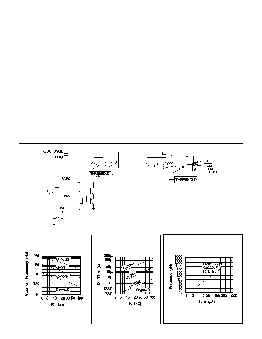
VARIABLE FREQUENCY OSCILLATOR
The VFO block is controlled through 4 pins: C
VFO
, l
VFO
,
Osc Dsbl (oscillator disable), and Trig (trigger input). Os-
cillator frequency is approximately:
Frequency = I
VFO
/(C
VFO
* 1V)
With a fixed capacitor and low voltage applied to Trig and
Osc Dsbl, frequency is linearly modulated by varying the
current into the l
VFO
pin.
The Trig and Osc Dsbl inputs are used to modify VFO op-
eration. If Osc Dsbl is held high, the oscillator will com-
plete the current cycle but wait until Osc Dsbl is returned
low to initiate a new cycle. If a pulse is applied to Trig dur-
ing a cycle, the oscillator will immediately initiate a new
cycle. Osc Dsbl has priority over Trig, but if a trigger pulse
is received while Osc Dsbl is high, the VFO will remember
the trigger pulse and start a new cycle as soon as Osc
Dsbl goes low.
Normally low trigger pulses are used to synchronize the
oscillator to a faster clock. Normally high trigger pulses
can also be used to synchronize to a slower clock.
ONE SHOT TIMER
The one shot timer performs three functions and is pro-
grammed by the RC pin. The first function is to control
output driver pulse width. Secondly, it clocks the toggle
flip-flop. Thirdly, it establishes the maximum allowable fre-
quency for the VFO. One shot operation is initiated at the
beginning of each oscillator cycle. The RC pin, pro-
grammed by an external resistor and capacitor to ground,
is charged to approximately 4.3V and then allowed to dis-
charge. The lower threshold is approximately 80% of the
peak. On time is approximately:
t(on) = 0.2 * R * C.
After crossing the lower threshold, the resistor continues
to discharge the capacitor to approximately 3V, where it
waits for the next oscillator cycle.
Maximum Frequency vs R
On Time vs R
VFO Frequency vs I
VFO
5
UC1860
UC2860
UC3860
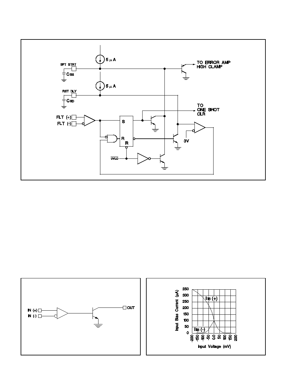
FAULT MANAGEMENT SECTION
During UVLO, the fault management section is initialized.
The latch is reset, and both Sft Strt (soft start) and Rst Dly
(restart delay) are pulled low. When Sft Strt is low, it low-
ers the upper clamp of the error amplifier. As Sft Strt in-
creases in voltage, the upper clamp increases from a
value equal to the lower clamp until it is 2V more positive.
A capacitor to ground from the Sft Strt pin will control the
start rate.
UNCOMMITTED COMPARATOR
The uncommitted comparator, biased from the reference
voltage, operates independently from the rest of the chip.
The open collector output is capable of sinking 2mA. The
inputs are valid in the common mode range of -0.3 to
3.0V. As long as one of the inputs is within this range, the
other can be as high as 5V.
The high speed fault comparator will work over the input
common mode range of -0.3 to 3.0V. When a fault is
sensed, the one shot is immediately terminated, Sft Strt is
pulled low, and Rst Dly is allowed to go high. Three
modes of fault disposition can easily be implemented. If
Rst Dly is externally held low, then a detected fault will
shut the chip down permanently. If the Rst Dly pin is left
open, a fault will simply cause an interruption of opera-
tion. If a capacitor is connected from Rst Dly to ground,
then hic-up operation is implemented. The hic-up time is:
t (off) = 600 kohm * C(Rst Dly).
Input Bias Current Input Voltage
6
UC1860
UC2860
UC3860
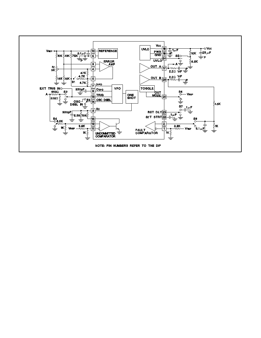
OPEN LOOP LABORATORY TEST FIXTURE
The open loop laboratory test fixture is designed to allow
familiarization with the operating characteristics of the
UC3860. Note the pin numbers apply to the DlP.
To get started, preset all the options as follows:
Adjust the error amplifier variable resistor pot (R1)
so the wiper is at a high potential.
Open the l
VFO
resistor switch (S1).
Throw the Trig switch (S2) to ground.
Throw the Osc Dsbl switch (S3) to ground.
Throw the uncommitted comparator switch (S4) to
ground.
Throw the UVLO switch (S5) to the resistive divider.
Throw the Out Mode switch (S6) to ground.
Open the restart delay switch (S7).
Throw the fault switch (S8)to ground.
In this configuration, the chip will operate for Vcc greater
than 12V. Adjustment of the following controls allows ex-
amination of specific features.
R1 adjusts the output of the error amp. Notice the voltage
at pin 5 is limited from 0 to 2V above the voltage at pin 7.
S1 changes the error amp output to VFO gain. With S1
open, the maximum frequency is determined by the error
amp output. With S1 closed, the one shot will set the
maximum frequency.
S2 demonstrates the trigger. An external trigger signal
may be applied. When the switch is set to the resistive di-
vider, the chip will operate in consecutive mode (ie: A,B,
off,...)
S3 allows input of an external logic signal to disable the
oscillator.
S4 demonstrates the uncommitted comparator. When set
to output A, the comparator will accelerate the discharge
of pin 9, shortening the output pulse.
S5 shorted to ground will disable the chip and the outputs
will be low. If the switch is open, the V
CC
start and stop
thresholds are 17 and 10V. Switched to the resistive di-
vider, the thresholds are approximately 12 and 10V.
S6 sets the mode of the toggle flip-flop. When grounded,
the outputs operate alternately. Switched to 5V, the out-
puts switch in unison. (Note: If S6 and S2 are set for uni-
son operation and triggered consecutive outputs, the chip
will free run at the maximum frequency determined by the
one shot.)
S7 open allows the chip to restart immediately after a
fault sense has been removed. When grounded, it causes
the chip to latch off indefinitely. This state can be reset by
UVLO, V
CC
, or opening the switch. Connected to I
µ
F pro-
grams a hic-up delay time of 600 ms.
S8 allows the simulation of a fault state. When flipped to
the RC network, the comparator monitors scaled average
voltage of output B. Adjusting frequency will cause the
comparator to sense a 'fault' and the chip will enter fault
sequence.
7
UC1860
UC2860
UC3860
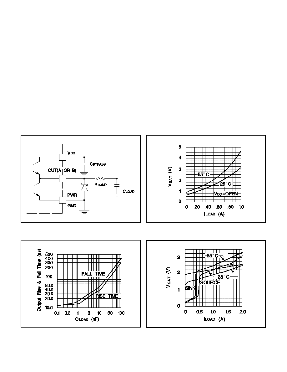
OUTPUT STAGE
The two totem pole output stages can be programmed by
Mode to operate alternately or in unison. When Mode is
low the outputs alternate. During UVLO, the outputs are
low.
Extreme care needs to be exercised in the application of
these outputs. Each output can source and sink transient
currents of 2A or more and is designed for high values of
dl/dt. This dictates the use of a ground plane, shielded in-
terconnect cables, Schottky diode clamps from the output
pins to Pwr Gnd (power ground), and some series resis-
tance to provide damping. Pwr Gnd should not exceed
±
0.2V from signal ground.
BYPASS NOTE
The reference should be bypassed with a 0.1
µ
F ceramic
capacitor from the V
REF
pin directly to the ground plane
near the Signal Ground pin. The timing capacitors on
C
VFO
and RC should be treated likewise. V
CC
, however,
should be bypassed with a ceramic capacitor from the
V
CC
pin to the section of ground plane that is connected
to Power Ground. Any required bulk reservoir capacitor
should parallel this one. The two ground plane sections
can then be joined at a single point to optimize noise re-
jection and minimize DC drops.
Output Saturation Voltage vs Load Current
Output Saturation Voltage vs Load Current
Output Rise & Fall Time vs Load Capacitance
UNITRODE INTEGRATED CIRCUITS
7 CONTINENTAL BLVD.
∑
MERRIMACK, NH 03054
TEL. 603-424-2410
∑
FAX 603-424-3460
8

IMPORTANT NOTICE
Texas Instruments and its subsidiaries (TI) reserve the right to make changes to their products or to discontinue
any product or service without notice, and advise customers to obtain the latest version of relevant information
to verify, before placing orders, that information being relied on is current and complete. All products are sold
subject to the terms and conditions of sale supplied at the time of order acknowledgement, including those
pertaining to warranty, patent infringement, and limitation of liability.
TI warrants performance of its semiconductor products to the specifications applicable at the time of sale in
accordance with TI's standard warranty. Testing and other quality control techniques are utilized to the extent
TI deems necessary to support this warranty. Specific testing of all parameters of each device is not necessarily
performed, except those mandated by government requirements.
CERTAIN APPLICATIONS USING SEMICONDUCTOR PRODUCTS MAY INVOLVE POTENTIAL RISKS OF
DEATH, PERSONAL INJURY, OR SEVERE PROPERTY OR ENVIRONMENTAL DAMAGE ("CRITICAL
APPLICATIONS"). TI SEMICONDUCTOR PRODUCTS ARE NOT DESIGNED, AUTHORIZED, OR
WARRANTED TO BE SUITABLE FOR USE IN LIFE-SUPPORT DEVICES OR SYSTEMS OR OTHER
CRITICAL APPLICATIONS. INCLUSION OF TI PRODUCTS IN SUCH APPLICATIONS IS UNDERSTOOD TO
BE FULLY AT THE CUSTOMER'S RISK.
In order to minimize risks associated with the customer's applications, adequate design and operating
safeguards must be provided by the customer to minimize inherent or procedural hazards.
TI assumes no liability for applications assistance or customer product design. TI does not warrant or represent
that any license, either express or implied, is granted under any patent right, copyright, mask work right, or other
intellectual property right of TI covering or relating to any combination, machine, or process in which such
semiconductor products or services might be or are used. TI's publication of information regarding any third
party's products or services does not constitute TI's approval, warranty or endorsement thereof.
Copyright
©
1999, Texas Instruments Incorporated