 | –≠–ª–µ–∫—Ç—Ä–æ–Ω–Ω—ã–π –∫–æ–º–ø–æ–Ω–µ–Ω—Ç: UC3864 | –°–∫–∞—á–∞—Ç—å:  PDF PDF  ZIP ZIP |

UC1861-1868
UC2861-2868
UC3861-3868
10/98
FEATURES
∑
Controls Zero Current Switched (ZCS)
or Zero Voltage Switched (ZVS)
Quasi-Resonant Converters
∑
Zero-Crossing Terminated One-Shot
Timer
∑
Precision 1%, Soft-Started 5V
Reference
∑
Programmable Restart Delay
Following Fault
∑
Voltage-Controlled Oscillator (VCO)
with Programmable Minimum and
Maximum Frequencies from 10kHz to
1MHz
∑
Low Start-Up Current (150
µ
A typical)
∑
Dual 1 Amp Peak FET Drivers
∑
UVLO Option for Off-Line or DC/DC
Applications
DESCRIPTION
The UC1861-1868 family of ICs is optimized for the control of Zero Cur-
rent Switched and Zero Voltage Switched quasi-resonant converters. Dif-
ferences between members of this device family result from the various
combinations of UVLO thresholds and output options. Additionally, the
one-shot pulse steering logic is configured to program either on-time for
ZCS systems (UC1865-1868), or off-time for ZVS applications (UC1861-
1864).
The primary control blocks implemented include an error amplifier to com-
pensate the overall system loop and to drive a voltage controlled oscillator
(VCO), featuring programmable minimum and maximum frequencies. Trig-
gered by the VCO, the one-shot generates pulses of a programmed maxi-
mum width, which can be modulated by the Zero Detection comparator.
This circuit facilitates "true" zero current or voltage switching over various
line, load, and temperature changes, and is also able to accommodate the
resonant components' initial tolerances.
Under-Voltage Lockout is incorporated to facilitate safe starts upon
power-up. The supply current during the under-voltage lockout period is
typically less than 150
µ
A, and the outputs are actively forced to the low
state.
(continued)
BLOCK DIAGRAM
Resonant-Mode Power Supply Controllers
UDG-92018
Pin numbers refer to the J and N packages.
Device
1861
1862
1863
1864
1865
1866
1867
1868
UVLO
16.5/10.5
16.5/10.5
36014
36014
16.5/10.5
16.5/10.5
36014
36014
Outputs
Alternating
Parallel
Alternating
Parallel
Alternating
Parallel
Alternating
Parallel
"Fixed"
Off Time
Off Time
Off Time
Off Time
On Time
On Time
On Time
On Time

2
UC1861-1868
UC2861-2868
UC3861-3868
ABSOLUTE MAXIMUM RATINGS
V
CC
. . . . . . . . . . . . . . . . . . . . . . . . . . . . . . . . . . . . . . . . . . . 22V
Output Current
Source or Sink (Pins 11 & 14) . . . . . . . . . . . . . . . . . . . . . 0.5A
DC Pulse (0.5
µ
s) . . . . . . . . . . . . . . . . . . . . . . . . . . . . . . . 1.5A
Power Ground Voltage . . . . . . . . . . . . . . . . . . . . . . . . . . .
±
0.2V
Inputs (Pins 2, 3, 10, & 15) . . . . . . . . . . . . . . . . . . . . ≠0.4 to 7V
Error Amp Output Current . . . . . . . . . . . . . . . . . . . . . . . .
±
2mA
Power Dissipation . . . . . . . . . . . . . . . . . . . . . . . . . . . . . . . . 1W
Junction Temperature (Operating). . . . . . . . . . . . . . . . . . 150
∞
C
Lead Temperature (Soldering, 10 seconds) . . . . . . . . . . 300
∞
C
All voltages are with respect to signal ground and all currents
are positive into the specified terminal. Pin numbers refer to
the J and N packages. Consult Unitrode Integrated Circuits da-
tabook for information regarding thermal specifications and
limitations of packages.
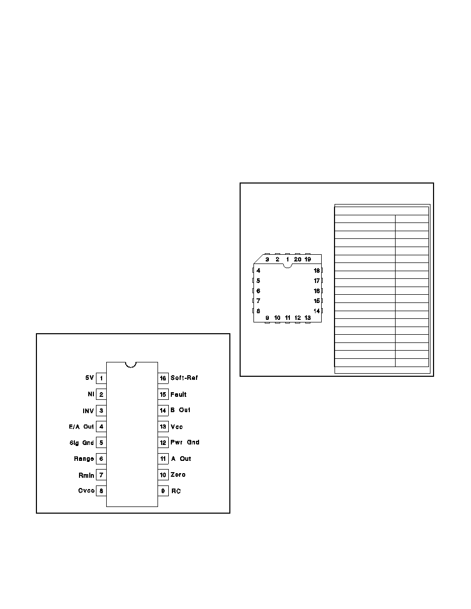
DIL-16, SOIC-16 (Top View)
J or N, DW Packages
CONNNECTION DIAGRAMS
PLCC-20 & LCC-20 (Top View)
Q & L Package
DESCRIPTION (cont.)
UVLO thresholds for the UC1861/62/65/66 are 16.5V
(ON) and 10.5V (OFF), whereas the UC1863/64/67/68
thresholds are 8V (ON) and 7V (OFF). After V
CC
ex-
ceeds the UVLO threshold, a 5V generator is enabled
which provides bias for the internal circuits and up to
10mA for external usage.
A Fault comparator serves to detect fault conditions and
set a latch while forcing the output drivers low. The Soft-
Ref pin serves three functions: providing soft start, re-
start delay, and the internal system reference.
Each device features dual 1 Amp peak totem pole output
drivers for direct interface to power MOSFETS. The out-
puts
are
programmed
to
alternate
in
the
UC1861/63/65/67 devices.
The UC1862/64/66/68 out-
puts operate in unison alllowing a 2 Amp peak current.
PACKAGE PIN FUNCTION
FUNCTION
PIN
Soft Ref
1
5V
2
NI
3
INV
4
E/A Out
5
Sig Gnd
6
Range
7
R
MIN
8
C
VCO
9
RC
10
Zero
11
NC
12
NC
13
A Out
14
Pwr Gnd
15
Pwr Gnd
16
V
CC
17
B Out
18

3
UC1861-1868
UC2861-2868
UC3861-3868
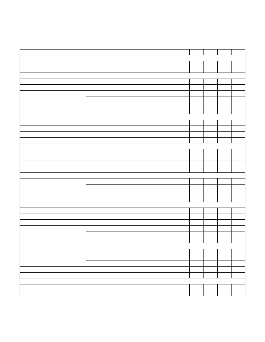
ELECTRICAL CHARACTERISTICS
Unless otherwise stated, all specifications apply for ≠55
∞
C
T
A
125
∞
C for the
UC186x, ≠25
∞
C
T
A
85
∞
C for the UC286x, and 0
∞
C
T
A
70
∞
C for the UC386x, V
CC
=12V, C
VCO
=1nF, Range=7.15k, R
MIN
=86.6k,
C=200pF, R=4.02k, and Csr=0.1
µ
F. T
A
=T
J .
PARAMETER
TEST CONDITIONS
MIN
TYP
MAX
UNITS
5V Generator
Output Voltage
12V
Vcc
20V, ≠10mA
I
O
0mA
4.8
5.0
5.2
V
Short Circuit Current
V
O
= 0V
≠150
≠15
mA
Soft-Reference
Restart Delay Current
V = 2V
10
20
35
µ
A
Soft Start Current
V = 2V
≠650
≠500
≠350
µ
A
Reference Voltage
T
J
= 25
∞
C, I
O
= 0A
4.95
5.00
5.05
V
12V
V
CC
20V, ≠200
µ
A
I
O
200
µ
A
4.85
5.15
V
Line Regulation
12V
V
CC
20V
2
20
mV
Load Regulation
≠200
µ
A
I
O
200
µ
A
10
30
mV
Error Amplifier (Note 3)
Input Offset Voltage
V
CM
= 5V, Vo = 2V, I
O
= 0A
≠10
10
mV
Input Bias Current
V
CM
= 0V
≠2.0
≠0.3
µ
A
Voltage Gain
Vcm = 5V, 0.5V
V
O
3.7V, I
O
= 0A
70
100
dB
Power Supply Rejection Ratio
Vcm = 5V, V
O
= 2V, 12V
V
CC
20V
70
100
dB
Error Amplifier (Note 3) (cont.)
Common Mode Rejection Ratio
0V
Vcm
6V, V
O
= 2V
65
100
dB
V
OUT
Low
V
ID
= ≠100mV, I
O
= 200
µ
A
0.17
0.25
V
V
OUT
High
V
ID
= 100mV, I
O
= ≠200
µ
A
3.9
4.2
V
Unity Gain Bandwidth
(Note 4)
0.5
0.8
MHz
Voltage Controlled Oscillator
Maximum Frequency
V
ID
(Error Amp) = 100mV, T
J
= 25
∞
C
450
500
550
kHz
V
ID
(Error Amp) = 100mV
425
575
kHz
Minimum Frequency
V
ID
(Error Amp) = ≠100mV, T
J
= 25
∞
C
45
50
55
kHz
V
ID
(Error Amp) = ≠100mV
42
58
kHz
One Shot
Zero Comparator Vth
0.45
0.50
0.55
V
Propagation Delay
(Note 4)
120
200
ns
Maximum Pulse Width
V
ZERO
= 1V
850
1000
1150
ns
Maximum to Minimum Pulse
V
ZERO
= 0V UCx861 ≠ UCx864
2.5
4
5.5
Width Ratio
V
ZERO
= 0V UCx865 ≠ UCx868. ≠55∞C to +85∞C
4
5.5
7
V
ZERO
= 0V UCx865 ≠ UCx868, +125∞C
3.8
5.5
7
Output Stage
Rise and Fall Time
C
LOAD
= 1nF (Note 4)
25
45
ns
Output Low Saturation
I
O
= 20mA
0.2
0.5
V
I
O
= 200mA
0.5
2.2
V
Output High Saturation
I
O
= ≠200mA, down from Vcc
1.7
2.5
V
UVLO Low Saturation
I
O
= 20mA
0.8
1.5
V
Fault Comparator
Fault Comparator Vth
2.85
3.00
3.15
V
Delay to Output
(Note 4) (Note 5)
100
200
ns

4
UC1861-1868
UC2861-2868
UC3861-3868
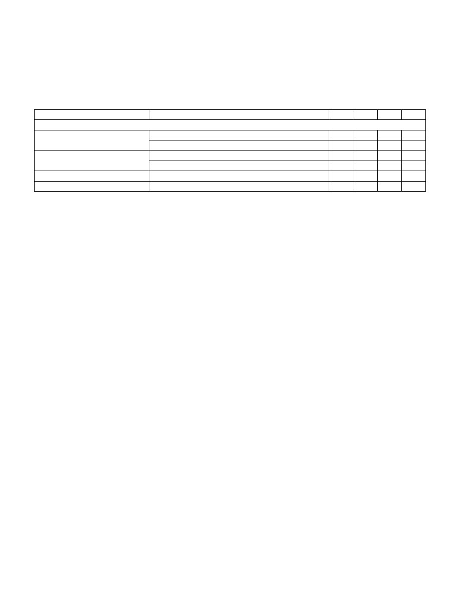
ELECTRICAL CHARACTERISTICS
Unless otherwise stated, all specifications apply for ≠55
∞
C
T
A
125
∞
C for the
UC186x, ≠25
∞
C
T
A
85
∞
C for the UC286x, and 0
∞
C
T
A
70
∞
C for the UC386x, V
CC
=12V, C
VCO
=1nF, Range=7.15k, R
MIN
=86.6k,
C=200pF, R=4.02k, and Csr=0.1
µ
F. T
A
=T
J .
PARAMETER
TEST CONDITIONS
MIN
TYP
MAX
UNITS
UVLO
Vcc Turn-on Threshold
UCx861, UCx862, UCx865, UCx866
15
16.5
18
V
UCx863, UCx864, UCx867, UCx868
7
8.0
9
V
Vcc Turn-off Threshold
UCx861, UCx862, UCx865, UCx866
9.5
10.5
11.5
V
UCx863, UCx864, UCx867, UCx868
6
7.0
8
V
Icc Start
V
CC
= V
CC
(on) ≠ 0.3V
150
300
µ
A
Icc Run
V
ID
= 100mV
25
32
mA
Note 1: Currents are defined as positive into the pin.
Note 2: Pulse measurement techniques are used to insure that T
J
= T
A
.
Note 3: VID = V(NI) ≠ V(INV).
Note 4: This parameter is not 100% tested in production but guaranteed by design.
Note 5: Vi = 0 to 4V tr(Vi)
10ns tpd = t(Vo = 6V) ≠ t(Vi = 3V)
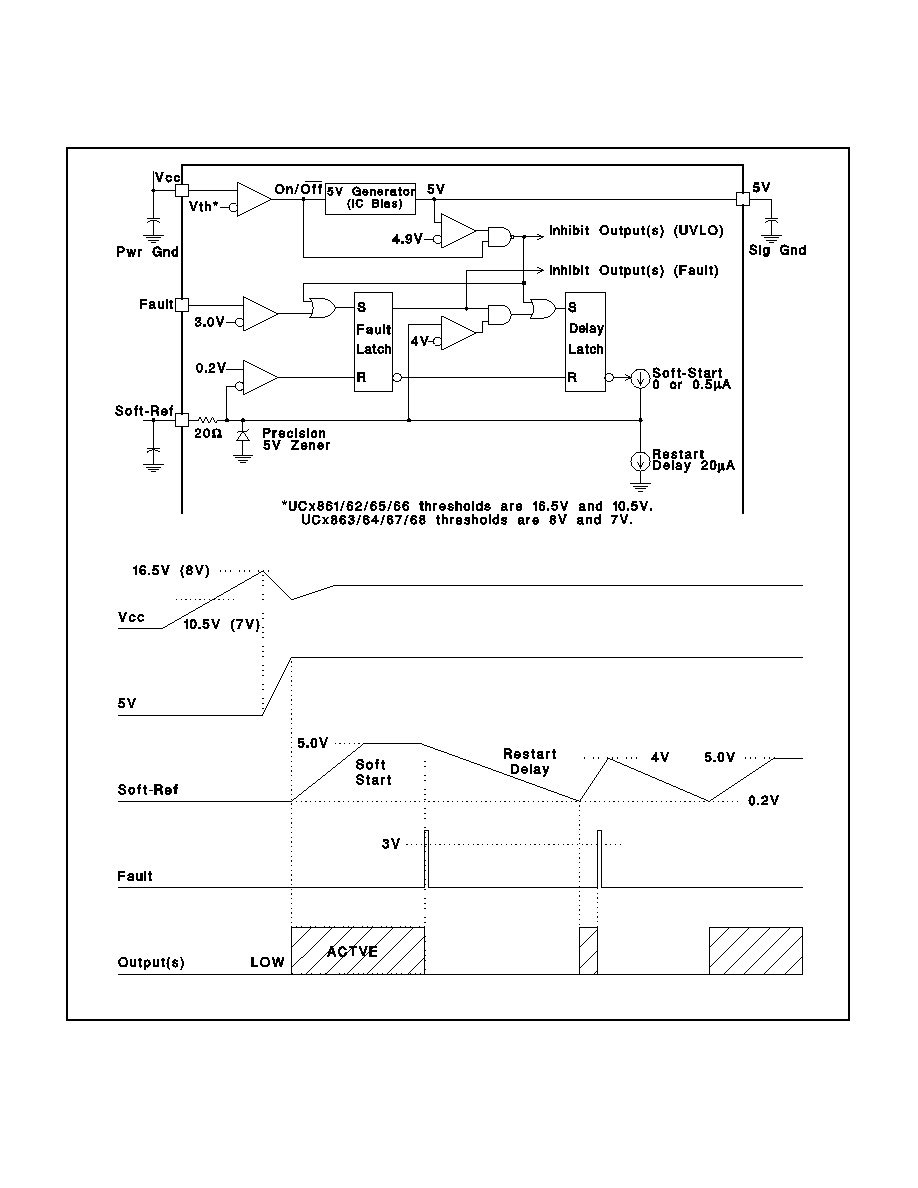
UVLO & 5V GENERATOR (See Figure 1): When power
is applied to the chip and Vcc is less than the upper
UVLO threshold, Icc will be less than 300
µ
A, the 5V gen-
erator will be off, and the outputs will be actively held low.
When Vcc exceeds the upper UVLO threshold, the 5V
generator turns on. Until the 5V pin exceeds 4.9V, the
outputs will still remain low.
The 5V pin should be bypassed to signal ground with a
0.1
µ
F capacitor. The capacitor should have low equiva-
lent series resistance and inductance.
FAULT AND SOFT-REFERENCE (See Figure 1): The
Soft-Ref pin serves three functions: system reference, re-
start delay, and soft-start. Designed to source or sink
200
µ
A, this pin should be used as the input reference for
the error amplifier circuit. This pin requires a bypass ca-
pacitor of at least 0.1
µ
F. This yields a minimum soft-start
time of 1ms.
Under-Voltage Lockout sets both the fault and restart de-
lay latches.
This holds the outputs low and discharges
the Soft-Ref pin. After UVLO, the fault latch is reset by
the low voltage on the Soft-Ref pin. The reset fault latch
resets the delay latch and Soft-Ref charges via the 0.5mA
current source.
The fault pin is input to a high speed comparator with a
threshold of 3V. In the event of a detected fault, the fault
latch is set and the outputs are driven low. If Soft-Ref is
above 4V, the delay latch is set. Restart delay is timed as
Soft-Ref is discharged by 20
µ
A. When Soft-Ref is fully
discharged, the fault latch is reset if the fault input signal
is low. The Fault pin can be used as a system shutdown
pin.
If a fault is detected during soft-start, the fault latch is set
and the outputs are driven low. The delay latch will re-
main reset until Soft-Ref charges to 4V. This sets the de-
lay latch, and restart delay is timed.
Note that restart
delay for a single fault event is longer than for recurring
faults since Soft-Ref must be discharged from 5V instead
of 4V.
The restart delay to soft-start time ratio is 24:1 for a fault
occurring during normal operation and 19:1 for faults oc-
curring during soft-start. Shorter ratios can be pro-
grammed down to a limit of approximately 3:1 by the
addition of a 20k
or larger resistor from Soft-Ref to
ground.
A 100k
resistor from Soft-Ref to 5V will have the effect
of permanent shut down after a fault since the internal
20
µ
A current source can't pull Soft-Ref low. This feature
can be used to require recycling Vcc after a fault. Care
must be taken to insure Soft-Ref is indeed low at start up,
or the fault latch will never be reset.
APPLICATION INFORMATION

5
UC1861-1868
UC2861-2868
UC3861-3868
APPLICATION INFORMATION
Figure 1. UVLO, 5V, fault and soft-ref.
UDG-92020
UDG-92021-1

6
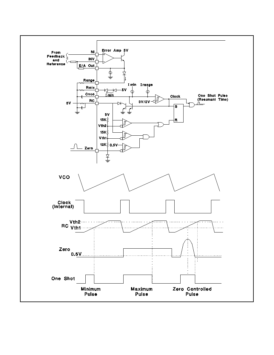
Figure 2. Error Amp, Voltage Controlled Oscillator, and One Shot
UDG-92022-1
UDG-92023-1

7
UC1861-1868
UC2861-2868
UC3861-3868
Minimum oscillator frequency is set by Rmin and Cvco.
The minimum frequency is approximately given by the
equation:
F
R
C
MIN
MIN
VCO
43
.
∑
Maximum oscillator frequency is set by Rmin, Range &
Cvco. The maximum frequency is approximately given by
the equation:
F
R
Range
C
MAX
MIN
VCO
3 3
.
(
/ /
)
∑
The Error Amplifier directly controls the oscillator fre-
quency. E/A output low corresponds to minimum fre-
quency and output high corresponds to maximum
frequency. At the end of each oscillator cycle, the RC pin
is discharged to one diode drop above ground. At the be-
ginning of the oscillator cycle, V(RC) is less than Vth1
and so the output of the zero detect comparator is ig-
nored. After V(RC) exceeds Vth1, the one shot pulse will
be terminated as soon as the zero pin falls below 0.5V or
V(RC) exceeds Vth2. The minimum one shot pulse width
is approximately given by the equation:
Tpw(min)
0.3
R
C.
The maximum pulse width is approximately given by:
Tpw(max)
1.2
R
C.
APPLICATION INFORMATION
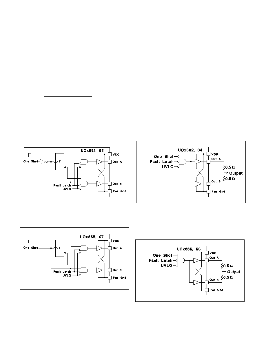
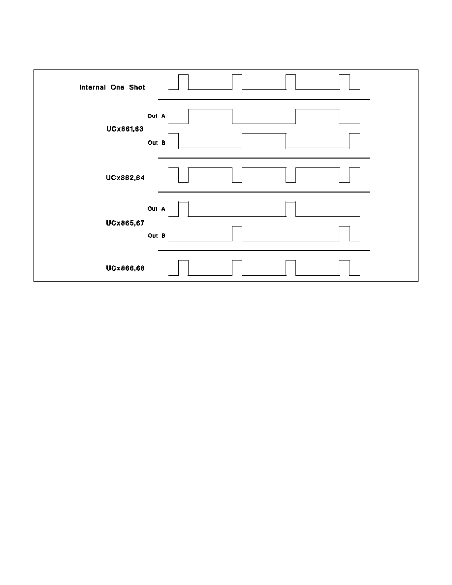
The steering logic is configured on the UC1861,63 to result in
dual non-overlapping square waves at outputs A & B. This is
suited to drive dual switch ZVS systems.
STEERING LOGIC
UDG-92013
The steering logic is configured on the UC1862,64 to result in
inverted pulse trains occurring identically at both output pins.
This is suited to drive single switch ZVS systems. Both outputs
are available to drive the same MOSFET gate. It is advisable
to join the pins with 0.5 ohm resistors.
UDG-92014
The steering logic is configured on the UC1865,67 to result in
alternating pulse trains at outputs A & B. This is suited to drive
dual switch ZCS systems.
UDG-92015
The steering logic is configured on the UC1866,68 to result in
non-inverted pulse trains occurring identically at both output
pins. This is suited to drive single switch ZCS systems. Both
outputs are available to drive the same MOSFET gate. It is ad-
visable to join the pins with 0.5 ohm resistors.
UDG-92016

8
UC1861-1868
UC2861-2868
UC3861-3868
APPLICATION INFORMATION (cont.)
Figure 3. Current waveforms.
UNITRODE CORPORATION
7 CONTINENTAL BLVD. ∑ MERRIMACK, NH 03054
TEL. (603) 424-2410 ∑ FAX (603) 424-3460
UDG-92017

IMPORTANT NOTICE
Texas Instruments and its subsidiaries (TI) reserve the right to make changes to their products or to discontinue
any product or service without notice, and advise customers to obtain the latest version of relevant information
to verify, before placing orders, that information being relied on is current and complete. All products are sold
subject to the terms and conditions of sale supplied at the time of order acknowledgement, including those
pertaining to warranty, patent infringement, and limitation of liability.
TI warrants performance of its semiconductor products to the specifications applicable at the time of sale in
accordance with TI's standard warranty. Testing and other quality control techniques are utilized to the extent
TI deems necessary to support this warranty. Specific testing of all parameters of each device is not necessarily
performed, except those mandated by government requirements.
CERTAIN APPLICATIONS USING SEMICONDUCTOR PRODUCTS MAY INVOLVE POTENTIAL RISKS OF
DEATH, PERSONAL INJURY, OR SEVERE PROPERTY OR ENVIRONMENTAL DAMAGE ("CRITICAL
APPLICATIONS"). TI SEMICONDUCTOR PRODUCTS ARE NOT DESIGNED, AUTHORIZED, OR
WARRANTED TO BE SUITABLE FOR USE IN LIFE-SUPPORT DEVICES OR SYSTEMS OR OTHER
CRITICAL APPLICATIONS. INCLUSION OF TI PRODUCTS IN SUCH APPLICATIONS IS UNDERSTOOD TO
BE FULLY AT THE CUSTOMER'S RISK.
In order to minimize risks associated with the customer's applications, adequate design and operating
safeguards must be provided by the customer to minimize inherent or procedural hazards.
TI assumes no liability for applications assistance or customer product design. TI does not warrant or represent
that any license, either express or implied, is granted under any patent right, copyright, mask work right, or other
intellectual property right of TI covering or relating to any combination, machine, or process in which such
semiconductor products or services might be or are used. TI's publication of information regarding any third
party's products or services does not constitute TI's approval, warranty or endorsement thereof.
Copyright
©
1999, Texas Instruments Incorporated

