 | –≠–ª–µ–∫—Ç—Ä–æ–Ω–Ω—ã–π –∫–æ–º–ø–æ–Ω–µ–Ω—Ç: UC3874L-2 | –°–∫–∞—á–∞—Ç—å:  PDF PDF  ZIP ZIP |
DESCRIPTION
The UC3874 family of synchronous step-down (Buck) regulators provides
high efficiency power conversion from an input voltage range of 4.5 to 36
volts. The UC3874 is tailored for battery powered applications such as
laptop computers, consumer products, communications systems, and
aerospace which demand high performance and long battery life. The
synchronous regulator replaces the catch diode in the standard buck
regulator with a low Rds(on) N-channel MOSFET switch allowing for
significant efficiency improvements. The high side N-channel MOSFET
switch is driven out of phase from the low side N-channel MOSFET switch
by an on-chip bootstrap circuit which requires only a single external
capacitor to develop the regulated gate drive. Fixed frequency, average
current
mode
control
provides
the
regulator
with
inherent
slope
compensation, tight regulation of the output voltage, and superior load and
line transient response. Switching frequencies up to 300kHz are possible.
Light load efficiency is improved by a fully programmable standby mode, in
which the quiescent current consumption of the controller is significantly re-
duced. The reduction is achieved by disabling the MOSFET driver outputs
and the internal oscillator when the controller has sensed that the the out-
put load current has dropped a user programmable amount from full load.
(continued)
High Efficiency, Synchronous, Step-down (Buck) Controllers
FEATURES
∑
Operation to 36V Input Voltage
∑
Fixed Frequency Average Current
Mode Control
∑
Standby Mode for Improved
Efficiency at Light Load
∑
Drives External N-Channel
MOSFETs for Highest Efficiency
∑
Sleep Mode Current < 50mA
∑
Complementary 1 Amp Outputs with
Regulated Gate Drive Voltage
∑
LDO (Low Drop Out) Virtual 100%
Duty Cycle Operation
∑
Non-Overlapping Gate Drives
SLUS286A - FEBRUARY 1998 - REVISED OCTOBER 2001
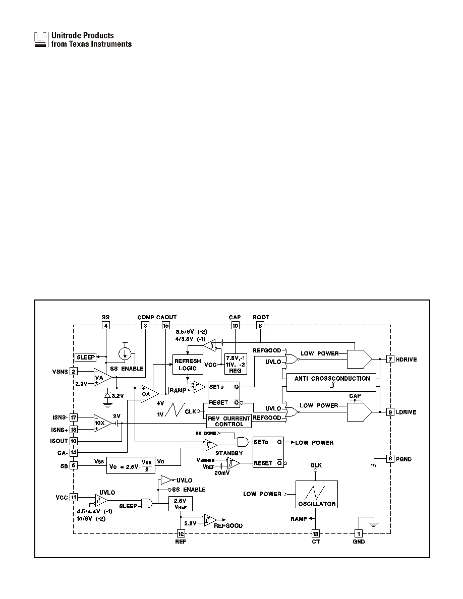
BLOCK DIAGRAM
UC1874-1,-2
UC2874-1,-2
UC3874-1,-2
UDG-95005-1
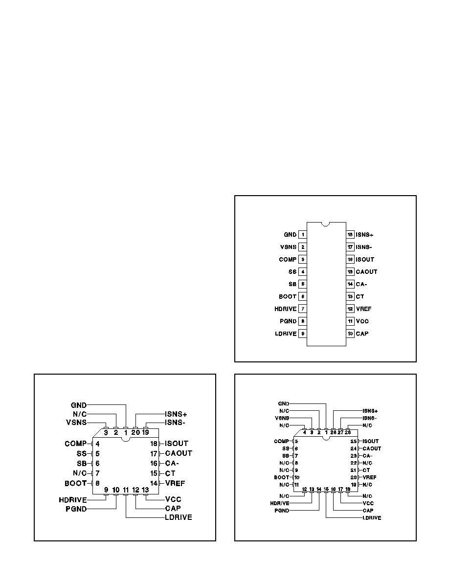
2
UC1874-1,-2
UC2874-1,-2
UC3874-1,-2
DIL-18 (TOP VIEW)
J or N, DW Packages
ABSOLUTE MAXIMUM RATINGS
Supply Voltage (VCC) . . . . . . . . . . . . . . . . . . . . . . . . . . . . . 36V
Boost Voltage (BOOT). . . . . . . . . . . . . . . . . . . . . . . . . . . . . 50V
OUTPUT Drivers (HDRIVE, LDRIVE) Currents
(continuous) . . . . . . . . . . . . . . . . . . . . . . . . . . . . . . . ±0.25A
(peak) . . . . . . . . . . . . . . . . . . . . . . . . . . . . . . . . . . . . . . . ±1A
VREF Current . . . . . . . . . . . . . . . . . . . . . . . . Internally Limited
Inputs (VSNS, SS, COMP, CT) . . . . . . . . . . . . . . . . -0.3 to 10V
Inputs (ISNS+, ISNS-) . . . . . . . . . . . . . . . . . . . . . . . -0.3 to 20V
Outputs (CAOUT) . . . . . . . . . . . . . . . . . . . . . . . . . . . -0.3 to10V
Soft start Sinking Current . . . . . . . . . . . . . . . . . . . . . . . . 1.5mA
Storage Temperature . . . . . . . . . . . . . . . . . . . ≠65∞C to +150∞C
Junction Temperature . . . . . . . . . . . . . . . . . . . ≠65∞C to +150∞C
Lead Temperature (Soldering, 10 sec.) . . . . . . . . . . . . . +300∞C
All currents are positive into, negative out of the specified ter-
minal. All voltages are referenced to GND. Consult Packaging
Section of Databook for thermal limitations and considerations
of packages.
CONNECTION DIAGRAMS
During standby operation, the output capacitor supplies
all of the load current requirements. Normal operation re-
turns when the output voltage has drooped by 1%. Re-
verse current in the inductor is prevented by on-chip
circuitry providing additional efficiency improvements.
Virtual 100% duty cycle operation is easily attained by
the controller even though a bootstrapped high side drive
technique is employed.
A low power sleep mode can be invoked through the SS
pin. Quiescent supply current in sleep mode is typically
less than 50mA. Two UVLO options are available. The
UC3874-1 is designed for logic level MOSFETs and has
UVLO turn-on and turn-off thresholds of 4.5V and 4.4V
respectively. The UC3874-2 is designed for standard
power MOSFETs and has UVLO turn-on and turn-off
thresholds of 10V and 9V respectively. A precision 2.5V
reference can supply 20mA to external circuitry. An error
amplifier with soft start, high bandwidth current amplifier,
and a synchronizable oscillator are additional features.
Available packages include 18-pin plastic and ceramic
DIP (N, J), 18-pin SOIC (DW), and 20-pin plastic and
ceramic leadless chip carriers (Q, L).
PLCC-20 (TOP VIEW)
Q Package
LCC-28 (TOP VIEW)
L Package
3
UC1874-1,-2
UC2874-1,-2
UC3874-1,-2
ELECTRICAL CHARACTERISTICS:
Unless otherwise stated these specifications apply for T
A
= ≠55∞C to +125∞C for
UC1874; T
A
= ≠25∞C to +85∞C for UC2874; 0∞C to +70∞C for UC3874; VCC = 12V, Ct = 680pF, C
CAP
= 1 F; C
BOOT
= 0.1 F;
T
A
= T
J
.
PARAMETER
TEST CONDITIONS
MIN
TYP
MAX
UNITS
Overall Section
Supply Current, Sleep
SOFTSTART = 0V; TA=25∞C
30
75
A
Supply Current, Operating
8.5
12
mA
Supply Current, Standby
UC2874-1, -2, UC3874-1, -2
2.5
3.5
mA
Supply Current, Standby
UC1874-1, -2
5.5
mA
V
CC
Turn-on Threshold
UCX874-2
10
10.5
V
UCX874-1
4.5
4.8
V
V
CC
Turn-off Threshold
UCX874-2
8.2
9
V
UCX874-1
4.1
4.4
V
Voltage Amplifier Section
Input Voltage
T
A
= 25∞C
1.97
2
2.03
V
VSNS Bias Current
≠500
25
500
nA
Transconductance
I
COM
p = +10 A to ≠10 A, UC3874 -1, -2;
UC2874-1, -2
400
675
1000
Mho
Transconductance
I
COM
p = +5 A to ≠5 A, UC1874-1,-2
250
675
1250
Mho
V
OUT
High
2.8
3.1
3.25
V
V
OUT
Low
SB = VREF
1.85
V
Output Source Current
V
OUT
= 1V; UC3874-1,-2; UC2874-1,-2
10
35
A
V
OUT
= 1V; UC1874 -1,-2
5
35
A
Current Amplifier Section
Input Offset Voltage
V
COMP
= 2.5V
≠6
0
6
mV
Input Bias Current (
SENSE
)
V
CM
= 2.5V
≠500
500
nA
Open Loop Gain
V
CM
= 2.5V, V
OUT
= 1V to 3.5V
80
110
dB
V
OUT
High
R
CAOUT
= 100k to GND, T
A
= 25∞C
3.6
3.7
V
V
OUT
Low
R
CAOUT
= 100k to VREF, T
A
= 25∞C
0.7
0.86
V
Output Source Current
V
OUT
= 0V, T
A
= 25∞C
80
100
120
A
Common Mode REJ Ratio
VCM = 2V to 3V
70
90
dB
Gain Bandwidth Product
F
IN
= 100kHz, 10mV p-p
2
3.5
MHz
Reference Section
Output Voltage
I
REF
= 0mA, T
A
= 25∞C
2.462
2.5
2.538
V
I
REF
= 0mA
2.437
2.5
2.563
V
Load Regulation
I
REF
= 0mA to 5mA
2
± 15
mV
Line Regulation
VCC = 12V to 24V
2
± 15
mV
Short Circuit Current
VREF = 0V
10
20
25
mA
Oscillator Section
Initial Accuracy
T
A
= 25∞C
85
100
115
kHz
Voltage Stability
V
CC
= 12V to 18V
1
1.5
%
Total Variation
Line, Temperature
80
120
kHz
Ramp Amplitude (p-p)
T
A
= 25∞C
2.48
2.7
2.85
V
Ramp Valley Voltage
T
A
= 25∞C
0.86
0.95
V
Sleep/Soft Start/Bootstrap Section
Sleep Threshold
Measured on SS, T
A
= 25∞C
0.25
0.6
0.8
V
SS Charge Current
V
SS
= 2.5V
4
6
10
A
SS Discharge Current
V
SS
= 2.5V
0.5
0.8
mA
4
UC1874-1,-2
UC2874-1,-2
UC3874-1,-2
ELECTRICAL CHARACTERISTICS:
Unless otherwise stated these specifications apply for T
A
= ≠55∞C to +125∞C for
UC1874; T
A
= ≠25∞C to +85∞C for UC2874; 0∞C to +70∞C for UC3874; VCC = 12V, Ct = 680pF, C
CAP
= 1 F; C
BOOT
= 0.1 F;
T
A
= T
J
.
PARAMETER
TEST CONDITIONS
MIN
TYP
MAX
UNITS
Sleep/Soft start/Bootstrap Section (continued)
Bootstrap Regulation Voltage
UCX874-2, Low Driver ON
9.5
10.2
12.5
V
UCX874-1, Low Driver ON
6
7.5
9
V
Bootstrap Refresh Voltage
UCX874-2, V
CAOUT
> V
CT
PEAK
7
8
9
V
UCX874-1, V
CAOUT
> V
CT
PEAK
2.7
3.5
4
V
High Side Driver Output Section
Output High Voltage
I
OUT
= ≠50mA, Boot = 23V
21
22.2
V
Output Low Voltage
I
OUT
= 50mA
1
2.2
V
I
OUT
= 10mA
300
500
mV
Output Low (UVLO)
I
OUT
= 50mA, VCC = 0V
0.9
1.5
V
Output Rise Time
C
OUT
= 1nF
40
160
ns
Output Fall Time
C
OUT
= 1nF
30
100
ns
Low Side Driver Output Section
Output High Voltage
I
OUT
= ≠50mA, V
CAP
= 11V
8.8
9.5
V
Output Low Voltage
I
OUT
= 50mA
1
2.2
V
I
OUT
= 10mA
300
500
mV
Output Low (UVLO)
I
OUT
= 50mA, VCC = 0V
0.9
1.5
V
Output Rise/Fall Time
C
LOAD
= 1nF
40
160
ns
Output Fall Time
C
OUT
= 1nF
30
100
ns
X10 Amplifier Section
Gain
V
ISNS
±
V
ISNS
= 20mV to 80mV
9.2
9.8
10.4
V/V
Slew Rate Rising
T
A
= 25∞C
1
1.4
V/ s
Slew Rate Falling
T
A
= 25∞C
2
3.5
V/ s
Input Resistance
T
A
= 25∞C
60
100
165
k
PIN DESCRIPTIONS
BOOT: This pin provides the high side rail for the
HDRIVE output.
An external capacitor (C
BST
) is
connected between this pin and the drain of the external
low side MOSFET.
When the low side MOSFET is
conducting Cbst is charged to 11V via an external diode
tied to CAP. When the low side MOSFET turns off and
the high side MOSFET turns on, the Cbst bootstraps
itself up with the source of high side MOSFET, ultimately
providing a 10V Vgs for the upper MOSFET. Since this
10V is referenced to the source of the high side
N-channel MOSFET, the actual voltage on BOOT and
HDRIVE is approximately 10V above VCC while the high
side MOSFET is conducting. The voltage on BOOT is
continuously
monitored
during
low
input
voltage
conditions when the duty cycle equals approximately
100% to insure that a sufficient gate drive level is being
supplied by the UC3874. If the voltage on BOOT falls
below 8V (UC3874-2) or 3.5V (UC3874-1), the IC forces
the low side driver to cycle itself on for the few cycles
required to replenish C
BST
. In this way, virtual 100% duty
cycle operation is provided.
CA-: This is the inverting input to the current amplifier.
Connect a series resistor and capacitor between this pin
and CAOUT to set the current loop compensation. An in-
put resistor between this pin and ISOUT provides the in-
ductor current sense signal to the amplifier and also
sets the high frequency gain of the amplifier. The com-
mon mode operating range for this input is between GND
and 4V. The normal range during operation is between
2V and 3V.
CAOUT: This is the output of the wide bandwidth current
amplifier and one of the inputs to the PWM duty cycle
comparator. The output signal generated by this amplifier
commands the PWM to force the correct duty cycle to
maintain output voltage in regulation. The output can
swing from 0.1V to 4V.

5
UC1874-1,-2
UC2874-1,-2
UC3874-1,-2
CAP: A capacitor is normally connected between this pin
and GND providing bypass for the internal 11V regulator.
Charge is transferred from this capacitor to C
BST
via an
external diode when the low side MOSFET is conducting.
If VCC
10V logic level MOSFETs are generally speci-
fied. CAP should then be shorted to VCC in conjunction
with a low VF Schottky to BOOT to maximize the gate
drive amplitude. This technique provides adequate gate
drive signal amplitudes with VCC as low as 4.5V.
For
high input voltage applications, a simple external shunt
zener regulator circuit can be connected to CAP, thereby
offloading power dissipation requirements from the IC to
an external transistor.
COMP: This is the output of the voltage amplifier. It pro-
vides the current command signal to the current ampli-
fier. The voltage is clamped to approximately 3.2V.
CT: A capacitor from CT to GND sets the PWM oscillator
frequency according to the following equation:
F
CT
=
∑
1
14250
Use a high quality ceramic capacitor with low ESL and
ESR for best results. A minimum CT value of 220pF in-
sures good accuracy and less susceptibility to circuit lay-
out parasitics. The oscillator and PWM are designed to
provide practical operation to 300kHZ.
GND: All voltages are measured with respect to this pin.
All bypass capacitors and timing components except
those listed under the PGND pin description should be
connected to this pin. Component leads should be as
short and direct as possible.
HDRIVE, LDRIVE: The outputs of the PWM are totem
pole MOSFET gate drivers on the HDRIVE and LDRIVE
pins. The outputs can sink approximately 1A and source
500mA. This characteristic optimizes the switching transi-
tions by providing a controlled dV/dT at turn-on and a
lower impedance at turn-off. These are complementary
outputs with a typical deadtime of 200ns. Internal cir-
cuitry prevents the possibility of simultaneous conduction
of the output MOSFETs (shoot through). HDRIVE is the
high side bootstrapped output. Its upper power supply rail
is the BOOT pin which means that its output will fly ap-
proximately 10V above VCC when the upper side of the
totem pole output is conducting. The power supply rail for
LDRIVE is CAP. As a result the Vgs of both gates are
regulated to approximately 10V if VCC is >11V. A series
resistor between these pins and the MOSFET gates of at
least 10 ohms can be used to control ringing. Addition-
ally, a low VF Schottky diode should be connected be-
tween these pins and GND to prevent substrate
conduction and possible erratic operation.
ISNS-: This is the inverting input to the X10 instrumenta-
tion amplifier. The common mode input range for this pin
extends from GND to VCC. A low value resistor in series
with the output inductor is connected between this pin
and ISNS+ to develop the current sense signal.
ISNS+: This is the non-inverting input to the X10 instru-
mentation amplifier. The common mode input range for
this pin extends from GND to VCC.
ISOUT: This is the output of the X10 instrumentation am-
plifier. The output voltage on this pin is level shifted 2V
above GND, such that if a 100mV differential input is ap-
plied across ISNS+ and ISNS-, the output will be 3V.
PGND: This is the high current ground for the IC. The
MOSFET driver transistors are referenced to this ground.
For best performance an external star ground connection
should be made between this pin, the source of the low
side MOSFET, the capacitor on CAP, the anodes of any
external Schottky clamp diodes and the output filter ca-
pacitor. As with all high frequency layouts, a ground
plane and short leads are highly recommended.
SB: The voltage on SB sets the output current level at
which standby mode is initiated. A voltage level from 0V
to 1V programs the threshold from 50% to 0% of full load
current. Full load current corresponds to a 100mV differ-
ential signal across the ISNS inputs. Since this is a
high impedance input, a voltage divider derived from
VREF may be used to program this level. Another possi-
ble use is to actively control this level with external cir-
cuitry to adaptively control converter efficiency. Tying SB
to VREF disables standby mode operation.
SS: A capacitor from this pin to GND in conjunction with
an internal 10mA current source provides a soft start
function for the IC. The voltage level on SS clamps the
output of the voltage amplifier through an internal buffer,
thus providing a controlled startup. The SS time is ap-
proximately:
C
V
V
V
A
SS
O
IN
∑
∑ 3
10
µ
Once the device has completed its soft start cycle, a low
power sleep mode can be invoked by pulling SS below
0.5V typically. In sleep mode, all of the device functions
are disabled except for those which are required to bring
the device out of sleep mode when SS is released. Typi-
cal sleep mode supply current is less than 50mA.
VCC: Positive supply rail for the IC. Bypass this pin to
GND with a 1mF low ESL/ESR ceramic capacitor. The
maximum voltage for VCC is 36V. The turn on voltage
level on VCC is 4.5V with 100mV of hysteresis for the
UC3874-1 and 10V with 1V of hysteresis for the
UC3874-2.
6
UC1874-1,-2
UC2874-1,-2
UC3874-1,-2
VREF: VREF is the output of the precision reference.
The output is capable of supplying 20mA to peripheral
circuitry and is internally short circuit current limited.
VREF is disabled and low whenever VCC is below the
UVLO threshold, and when SS is pulled below 0.5V. A
VREF "good" comparator senses VREF and disables the
PWM stage until VREF has attained approximately 90%
of its nominal value. Bypass VREF to GND with a 0.1mF
ceramic capacitor for best performance.
VSNS: This pin is the inverting input of the voltage ampli-
fier and serves as the output voltage feedback point for
the synchronous regulator. It senses the output voltage
through a voltage divider which produces a nominal 2.0V.
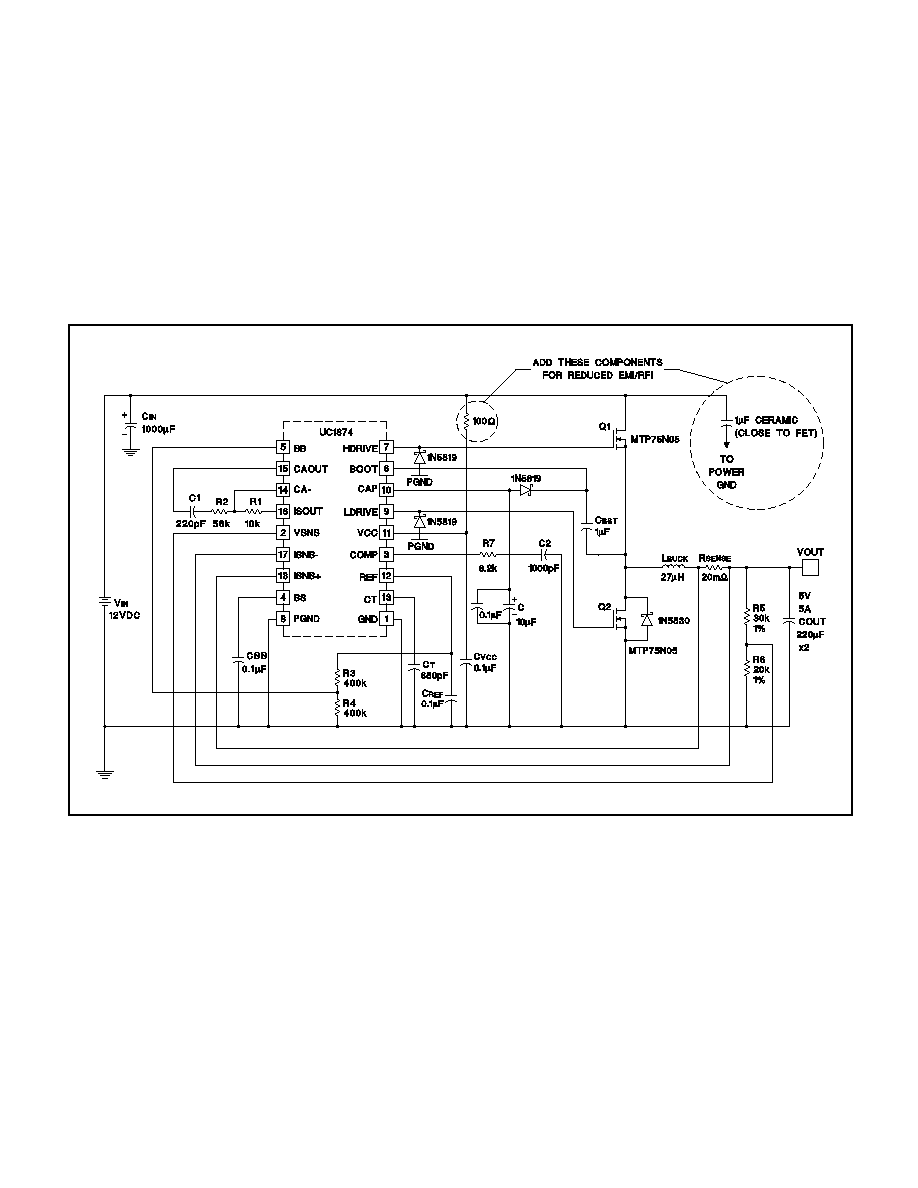
OPERATION: Refer to 5V, 25W Application Schematic
The UC3874 employs a fixed frequency average current
mode control buck topology to convert a higher battery
voltage down to a tightly regulated output voltage.
Spe-
cial design techniques allow this bipolar IC to deliver ex-
ceptional performance while consuming approximately
6mA of supply current over an input voltage range of 4.5
to 35 volts. Fixed frequency operation allows synchroni-
zation to an existing system clock, and easier filtering.
Average current mode control provides inherent slope
compensation and accurate short circuit current limiting.
An additional benefit is its ability to maintain a constant
regulator gain regardless of whether the inductor current
is continuous or discontinuous.
The output inductor current is sensed by an external low
value shunt resistor (Rsense).
This signal at full load
current should be no larger than 100mV in order to mini-
mize sensing losses. The differential voltage across
Rsense is amplified by the internal X10 instrumentation
amplifier. The common mode input range for this ampli-
fier extends from GND to VCC in order to maintain accu-
rate current sensing under normal conditions as well as
abnormal conditions such as output short circuit and low
drop out (LDO) modes. The output of the X10 instrumen-
tation amplifier is applied to the inverting input of the cur-
rent
amplifier
through
an
external
resistor.
The
converter's output voltage feedback is applied to the
APPLICATION DIAGRAM
UDG-95006-1

7
UC1874-1,-2
UC2874-1,-2
UC3874-1,-2
VSNS pin through an external voltage divider. The differ-
ence between the voltage at VSNS and the internal ref-
erence level at the non-inverting input is amplified by the
voltage amplifier and applied to the non-inverting input of
the current amplifier. This instantaneous reference level
forms the current command input for the average current
control loop. The average current amplifier develops the
duty cycle command signal by integrating the current
feedback signal with respect to the instantaneous current
command input. This output is compared to the fixed
high amplitude oscillator ramp waveform at the inputs of
the PWM comparator to develop duty cycle information
for the PWM drive. The large amplitude oscillator ramp
provides both high noise margin and built-in slope com-
pensation in average current mode control methodology.
The fixed frequency oscillator is programmed with a sin-
gle external capacitor connected between CT and GND,
and is capable of switching frequencies up to 300kHz.
The UC3874 can be synchronized to an external clock
by capacitively coupling the signal to the junction of the
capacitor at CT and a low value resistor tied to GND. Re-
fer to Application Note U-111.
The PWM drive signal is applied to the complementary
output driver stages. Since the high side switch is an N-
channel MOSFET, a means for driving its gate above
VCC is required. This is accomplished via the internal
11V regulator and an external capacitor (C
BST
). C
BST
is
charged through an external diode to VCC or CAP when
the low side MOSFET is on. The charging level on Cbst
is internally regulated to 11V minus an external diode
drop by the UC3874 as long as VCC is above 11V. When
the low side MOSFET turns off, C
BST
is applied across
the gate to the source of the upper MOSFET allowing it
to begin turn-on. As the upper MOSFET turns on, it lifts
or bootstraps the low end of C
BST
, along with its source.
Shortly thereafter, the source voltage level is reduced by
RDS(on) ∑ Iload below VCC. When VCC < 10V, Vgs for
the high side MOSFET is approximately equal to VCC. If
VCC < 8V, logic level MOSFETs are recommended. In
these applications, CAP should be shorted to VCC and
an external Schottky diode is connected between
CAP/VCC and BOOT. For low battery applications, a syn-
chronous regulator must be capable of LDO or 100%
duty cycle operation. The UC3874 includes circuitry to
insure that this mode of operation is possible even
though it uses a bootstrapped drive technique for the
high side MOSFET. During commanded 100% duty cycle
operation, the UC3874 monitors the Vgs drive signal ap-
plied to the high side MOSFET, and automatically pro-
vides complementary pulses to refresh the bootstrap
capacitor when this voltage falls below a set threshold. In
this way, near 100% duty cycle operation is possible, with
effective duty cycle dependent only upon the value of
C
BST
.
High efficiency is obtained primarily by the low side
MOSFET which replaces the Schottky diode in the stan-
dard buck configuration. Its low Rds(on) produces a
much lower voltage drop than a low VF Schottky diode.
As output voltages get lower, these improvements be-
come more evident. Additional efficiency improvements
at light regulator load currents are obtained by automatic
switchover to standby mode. In standby mode, the
UC3874 disables its MOSFET drivers and oscillator sav-
ing both quiescent supply current consumption and more
importantly MOSFET gate drive charge current. Standby
mode is initiated when the output inductor current has
dropped to a user programmable fraction of the designed
full load current. Programmability is easily attained by
setting the SB pin to a voltage level between 0V and 1V,
which corresponds to 50% to 0% of the peak load cur-
rent. In this manner, the user can accurately determine
when standby mode is initiated, giving the flexibility to di-
rectly shape the efficiency vs. load curve. In standby
mode, all output current requirements are handled by the
output capacitor. Since the output capacitor isn't being
refreshed by the PWM converter, the output voltage will
decay at a rate determined by the load current and the
output capacitor value:
d V
d T
I
C
LOAD
OUT
=
Normal operation returns when the output voltage has
decayed by approximately 1% from its nominal value.
Standby operation can be easily disabled by connecting
the SB pin directly to VREF. Another efficiency consid-
eration is the the possibility of reverse current in the out-
put inductor. For a non-synchronous regulator this isn't a
problem since the diode will block reverse current, allow-
ing discontinuous inductor current operation at light
loads. Since the synchronous regulator replaces the di-
ode with a switch, reverse current can and will flow if the
low side switch is on when the inductor is depleted. The
UC3874 includes circuitry to prevent reverse current from
flowing in the inductor by disabling the low side gate
drive signal during discontinuous mode operation. This
increases efficiency by eliminating unnecessary I2R
losses in the MOSFET and the inductor.
Soft start is recommended for Buck converters to reduce
stress on the power components during startup, and to
reduce overshoot of the output voltage. This improves
reliability. The UC3874 includes a user programmable
soft start pin to implement this feature. An internal 10mA
current source charges the external soft start capacitor
which provides a clamp at the output of the voltage
8
UC1874-1,-2
UC2874-1,-2
UC3874-1,-2
amplifier. An ultra low power sleep mode is also invoked
from the SS pin. A voltage level below 0.5V on this pin
reduces total standby current to less than 50mA. Short
circuit protection is inherent to the average current mode
technique with proper compensation of the current
amplifier. To prevent operation of the MOSFETs with an
inadequete drive signal, an undervoltage lockout circuit
suppresses the output drivers until the input supply
voltage is sufficiently high enough for proper operation.
The UC3874-1 is intended for applications with logic
level MOSFETs and its VCC turn-on and turn-off
thresholds are 4.5V/4.4V respectively. The UC3874-2 is
intended for applications with standard MOSFETs and
has UVLO turn-on and turn-off thresholds of 10V and 9V
respectively. The precision 2.5V reference can provide
20mA to power external circuitry. The reference output is
disabled during UVLO and sleep modes.
UC
874
≠
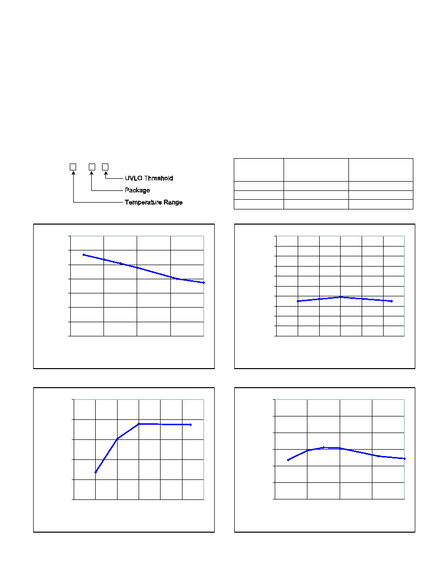
ORDERING INFORMATION
UVLO Turn
On/Off
Threshold
Package
Temperature
Range
1: 4.5V/4.4V
J: Ceramic DIL-18
1: ≠55∞C to +125∞C
2: 10V/9V
N: Plastic DIL-18
2: ≠40∞C to +85∞C
DW: SOIC-18
3: 0∞C to +70∞C
4
5
6
7
8
9
10
11
-75
-25
25
75
125
TEMPERATURE ∞C
I
CC
(mA)
TYPICAL PERFORMANCE INFORMATION
Figure 1. Supply Current
1.95
1.96
1.97
1.98
1.99
2
2.01
2.02
2.03
2.04
2.05
-50
-25
0
25
50
75
100
TEMPERATURE ∞C
VO
L
T
S
Figure 2. V
AMP
Input Voltage
80
90
100
110
120
130
140
-75
-25
25
75
125
TEMPERATURE ∞C
FREQ
UENCY
(KHz)
Figure 4. Oscillator Frequency vs. Temperature
(CT = 680pF)
560
600
640
680
720
760
-50
-25
0
25
50
75
100
TEMPERATURE ∞C
TRANSCONDUCT
ANCE
(uMho)
Figure 3. Volt Amp GM (I
OUT
=
10 A)
9
UC1874-1,-2
UC2874-1,-2
UC3874-1,-2
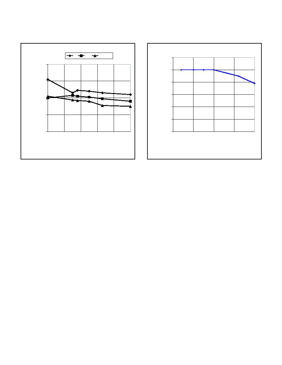
0.08
0.1
0.12
0.14
0.16
0
1
2
3
4
5
VCM (V)
VSC
(V)
0
70
ROOM
PERFORMANCE INFORMATION (continued)
Figure 5. Short Circuit Limit Voltage Reflected to
Input of Current Amp vs. Current Amp Common
Mode Voltage
75
80
85
90
95
100
105
-75
-25
25
75
125
TEMPERATURE ∞C
%
DUTY
C
YCLE
Figure 6. High Drive Maximum Duty Cycle
(UC1874-1,-2)

IMPORTANT NOTICE
Texas Instruments Incorporated and its subsidiaries (TI) reserve the right to make corrections, modifications,
enhancements, improvements, and other changes to its products and services at any time and to discontinue
any product or service without notice. Customers should obtain the latest relevant information before placing
orders and should verify that such information is current and complete. All products are sold subject to TI's terms
and conditions of sale supplied at the time of order acknowledgment.
TI warrants performance of its hardware products to the specifications applicable at the time of sale in
accordance with TI's standard warranty. Testing and other quality control techniques are used to the extent TI
deems necessary to support this warranty. Except where mandated by government requirements, testing of all
parameters of each product is not necessarily performed.
TI assumes no liability for applications assistance or customer product design. Customers are responsible for
their products and applications using TI components. To minimize the risks associated with customer products
and applications, customers should provide adequate design and operating safeguards.
TI does not warrant or represent that any license, either express or implied, is granted under any TI patent right,
copyright, mask work right, or other TI intellectual property right relating to any combination, machine, or process
in which TI products or services are used. Information published by TI regarding third≠party products or services
does not constitute a license from TI to use such products or services or a warranty or endorsement thereof.
Use of such information may require a license from a third party under the patents or other intellectual property
of the third party, or a license from TI under the patents or other intellectual property of TI.
Reproduction of information in TI data books or data sheets is permissible only if reproduction is without
alteration and is accompanied by all associated warranties, conditions, limitations, and notices. Reproduction
of this information with alteration is an unfair and deceptive business practice. TI is not responsible or liable for
such altered documentation.
Resale of TI products or services with statements different from or beyond the parameters stated by TI for that
product or service voids all express and any implied warranties for the associated TI product or service and
is an unfair and deceptive business practice. TI is not responsible or liable for any such statements.
Mailing Address:
Texas Instruments
Post Office Box 655303
Dallas, Texas 75265
Copyright
2001, Texas Instruments Incorporated