 | –≠–ª–µ–∫—Ç—Ä–æ–Ω–Ω—ã–π –∫–æ–º–ø–æ–Ω–µ–Ω—Ç: UC3886DTR | –°–∫–∞—á–∞—Ç—å:  PDF PDF  ZIP ZIP |
UC2886
UC3886
SLUS231 - JUNE 1998
Average Current Mode PWM Controller IC
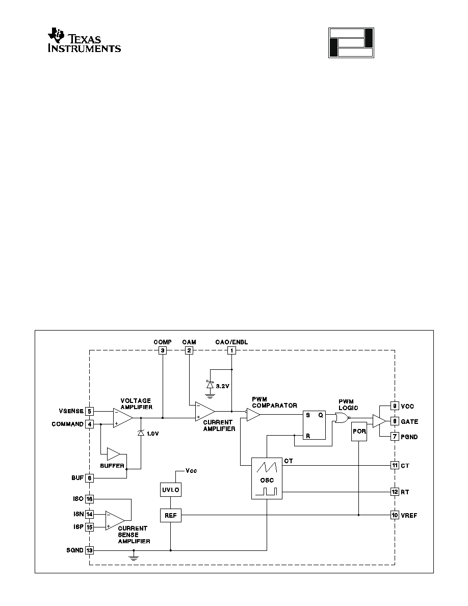
BLOCK DIAGRAM
UDG-95098-2
application
INFO
available
DESCRIPTION
The UC3886 family of PWM controller ICs is designed for DC-to-DC con-
verters with average current mode control. It is designed for use in con-
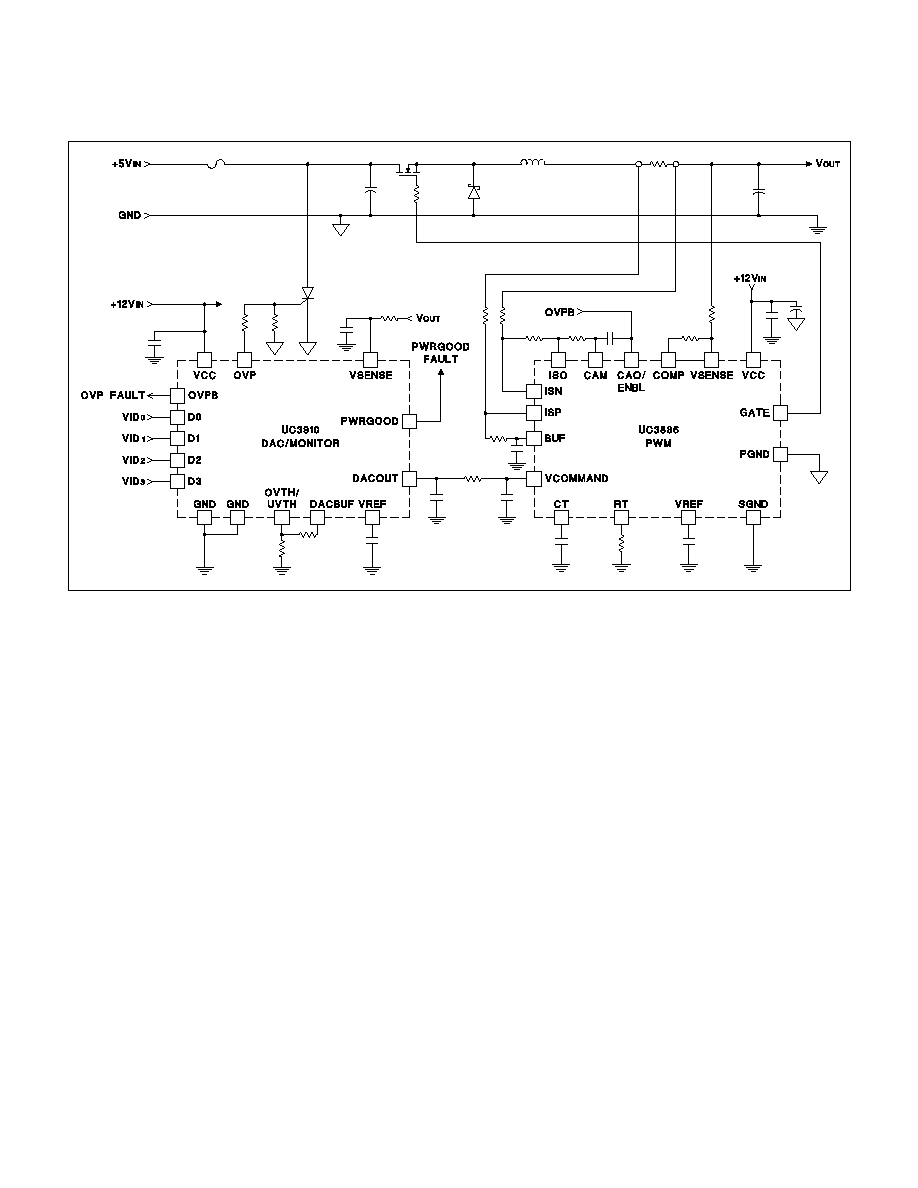
junction with the UC3910 4-bit DAC and Voltage Monitor. The UC3886
drives an external N-channel MOSFET and can be used to power the In-
tel PentiumÆ Pro and other high-end microprocessors.
The UC3886 in conjunction with the UC3910 converts 5VDC to an adjust-
able output ranging from 2.0V to 3.5V in 100mV steps with 35mV DC sys-
tem accuracy.
The oscillator is programmed by the user's selection of an external resis-
tor and capacitor, and is designed for 300kHz typical operation.
The voltage and current amplifiers have 3.5MHz gain-bandwidth product
to satisfy high performance system requirements.
The internal current sense amplifier permits the use of a low value current
sense resistor, minimizing power loss. It has inputs and outputs accessi-
ble to allow user-selection of gain-setting resistors, and is internally com-
pensated for a gain of 5 and above. The command voltage input is
buffered and provided for use as the reference for the current sense am-
plifier.
The output of the voltage amplifier (input to the current amplifier) is
clamped to 1 volt above the command voltage to serve as a current limit.
The gate output can be disabled by bringing the CAO/ENBL pin to below
0.8 volts.
FEATURES
∑
10.3V - 20V Operating Range
∑
Low Offset Voltage Amplifier
∑
High Bandwidth Current and Voltage
Amplifiers
∑
Low Offset Current Sense Amplifier
∑
Undervoltage Lockout
∑
Trimmed 5 Volt Reference
∑
Externally Programmable Oscillator
Charge Current
∑
1.5A Peak Totem Pole Output
∑
Available in 16-pin DIL or SOIC
Packages

2
UC2886
UC3886
CONNECTION DIAGRAM
DIL-16, SOIC-16 (Top View)
N or D Packages
ABSOLUTE MAXIMUM RATINGS
Supply Voltage . . . . . . . . . . . . . . . . . . . . . . . . . . . . . . . . . . 20V
Output Current
CAM, COMMAND, VSENSE, ISN, ISP . . . . . . . . . . . . . ± 1A
Analog Input . . . . . . . . . . . . . . . . . . . . . . . . . . . . . . ≠0.3V to 7V
Storage Temperature . . . . . . . . . . . . . . . . . . . ≠65∞C to +150∞C
Junction Temperature . . . . . . . . . . . . . . . . . . . ≠55∞C to +150∞C
Lead Temperatue (Soldering, 10 sec.) . . . . . . . . . . . . . +300∞C
Currents are positive into, negative out of the specified terminal.
Consult Packaging Section of Databook for thermal limitations
and considerations of packages.
ELECTRICAL CHARACTERISTICS
Unless otherwise specified, VCC = 12V, V
COMMAND
= 3.0V, CT = 1nF, RT = 10k,
T
A
= T
J
= 0∞C < T
A
< 70∞C for the UC3886
.
(Note: ≠25∞C < T
A
< 85∞C for the UC2886,
PARAMETER
TEST CONDITIONS
MIN
TYP
MAX
UNITS
Overall
Supply Current
VCC = 11V, Gate Open
10
15
mA
VCC = 9.3V
5
mA
Undervoltage Lockout
Start Threshold
9.7
10.3
10.8
V
UVLO Hysteresis
0.25
0.4
V
Voltage Error Amplifier
Input Offset Voltage
V
CM
= 3.0V (UC3886)
4
mV
V
CM
= 3.0V (UC2886)
15
mV
Input Bias Current
V
CM
= 3.0V
-
2
µ
A
Input Offset Current
V
CM
= 3.0V (UC3886)
0.01
µ
A
V
CM
= 3.0V (UC2886)
0.1
µ
A
Open Loop Gain
2.5V < V
COMP
< 3.5V
60
85
dB
Common-Mode Rejection Ratio
2V < V
COMP
< 4V
60
85
dB
Power Supply Rejection Ratio
11V < VCC < 15V
60
85
dB
Output High Voltage (Clamp)
I
COMP
= ≠100
µ
A (UC3886)
3.95
4
4.05
V
I
COMP
= ≠100
µ
A (UC2886)
3.9
4.1
V
Output Low Voltage (Clamp)
I
COMP
= 100
µ
A
1.9
2.7
V
Output Sink Current
V
COMP
= 3.7V
0.9
mA
Output Source Current
V
COMP
= 2.8V
≠0.15
-
0.25
mA
Gain-Bandwidth Product
F = 100kHz
2
3.5
MHz
5.0V Reference
Output Voltage
I
VREF
= 1.0mA
4.9
5
5.1
V
Total Variation
Line, Load, Temperature
4.825
5.175
V
Line Regulation
11V < VCC < 15V
10
mV
Load Regulation
0 < I
VREF
< 2mA
15
mV
Short Circuit Current
≠10
-
40
mA
3
UC2886
UC3886
ELECTRICAL CHARACTERISTICS
Unless otherwise specified, VCC = 12V, V
COMMAND
= 3.0V, CT = 1nF, RT = 10k,
T
A
= T
J
= 0∞C < T
A
< 70∞C for the UC3886
.
(Note: ≠25∞C < T
A
< 85∞C for the UC2886,
PARAMETER
TEST CONDITIONS
MIN
TYP
MAX
UNITS
Input Buffer
Gain
I
BUF
= ± 500
µ
A (UC3886)
0.98
1
1.02
V/V
I
BUF
= ± 500
µ
A (UC2886)
0.95
1.05
V/V
Current-Sense Amplifier
Input Offset Voltage
V
CM
= 3.0V (UC3886)
2
mV
V
CM
= 3.0V (UC2886)
6
mV
Input Bias Current
V
CM
= 3.0V
-1
µ
A
Input Offset Current
V
CM
= 3.0V
0.2
µ
A
Open Loop Gain
2V < V
ISO
< 6V
60
85
dB
CMRR
0V < V
CM
< 4.5V
60
85
dB
PSRR
11V < VCC < 15V
60
85
dB
Output High Voltage
I
ISO
= ≠100
µ
A
5
V
Output Low Voltage
I
ISO
= 1mA
1
V
Output Source Current
V
ISO
= 2V
-
0.2
mA
Gain-Bandwidth Product
F = 100kHz
2
3.5
MHz
Current Amplifier
Input Offset Voltage
V
CM
= 3.0V (UC3886)
13
mV
V
CM
= 3.0V (UC2886)
18
mV
Input Bias Current
V
CM
= 3.0V
1
µ
A
Open Loop Gain
1V < V
CAO
< 3V
60
85
dB
CMRR
1.5V < V
CM
< 4.5V
60
85
dB
PSRR
11V < VCC < 15V
60
85
dB
Output High Voltage
I
CAO
= ≠100
µ
A
3
3.3
V
Output Low Voltage
I
CAO
= 100
µ
A
1
V
Output Source Current
V
CAO
=1V
-
0.1
≠0.25
mA
Gain-Bandwidth Product
F = 100kHz
2
3.5
MHz
Oscillator
Frequency
RT = 10k, CT = 1nF (UC3886)
90
100
110
kHz
RT = 10k, CT = 1nF (UC2886)
85
115
kHz
Frequency Change With Voltage
11V > VCC > 15V
1
%
CT Peak Voltage
2.6
2.8
V
CT Valley Voltage
1
1.2
V
CT Peak-to-Peak Voltage
1.6
1.8
2.0
V
Output Section
Output Low Voltage
I
GATE
= 200mA
1.6
2.2
V
Output High Voltage
I
GATE
= ≠200mA
9
10.3
V
Output Low Voltage
5V < VCC < 9V, I
GATE
= 10mA
0.5
V
V
CAO
< 0.8V, I
GATE
= 10mA
0.5
V
Rise/Fall Time
C
L
= 1nF
150
ns
Maximum Duty Cycle
(UC3886)
90
%
(UC2886)
85
%

4
UC2886
UC3886
BUF: (Buffer Output) The voltage on COMMAND pin is
buffered and presented to the user here. This voltage is
used to provide the operating bias point for the current
sense amplifier by connecting a resistor between BUF
and ISP. Decouple BUF with 0.01
µ
F or greater to SGND.
CAM: (Current Amplifier Minus Input) The average load
current feedback from ISO is typically applied through a
resistor here.
CAO/ENBL: (Current Amplifier Output/Chip Enable) The
current loop compensation network is connected be-
tween CAO/ENBL and CAM, the inverting input of the
current amplifier. The voltage at CAO/ENBL is the input
to the PWM comparator and regulates the output voltage
of the system. The GATE output is disabled (held low)
unless the voltage at this pin exceeds 1.0 volts, allowing
the PWM to force zero duty cycle when necessary. The
user can force this pin below 0.8 volts externally with an
open collector, disabling the GATE drive.
COMMAND: (Voltage Amplifier Non-Inverting Input) This
input to the voltage amplifier is connected to a command
voltage, such as the output of a DAC. This voltage sets
the switching regulator output voltage.
COMP: (Compensation, Voltage Amplifier Output) The
system voltage compensation network is applied be-
tween COMP and VSENSE. The voltage at COMP is
clamped to prevent it from going more than 1V above the
COMMAND voltage. This is used to provide an accurate
average current limit. The voltage on COMP is also
clamped to 0.7V below the voltage on COMMAND. This
is done to avoid applying a full charge to capacitors in
the compensation network during transients, allowing
quick recovery time and little overshoot.
CT: (Oscillator Timing Capacitor) A capacitor from CT to
SGND along with the resistor on RT, sets the PWM fre-
quency and maximum duty cycle according to these
formulas:
D
V
RT
mA
MAX
=
∑
1
2 0
4 0
≠
.
.
where D
MAX
is the maximum operating duty cycle, and
RT is in ohms.
(
)
(
)
F
V
mA RT
V
CT
V
RT
mA
OSC
=
∑
∑
∑
∑
∑
2 0
4 0
2 0
1 8
4 0
2
.
.
≠ .
.
.
where F
OSC
is the UC3886 oscillator switching fre-
quency in Hz, RT is in ohms, and CT is in farads.
GATE: (PWM Output) The output is a 1A totem pole
driver. Use a series resistor of at least 5
to prevent in-
teraction between the gate impedance and the output
driver that might cause excessive overshoot.
ISN: (Current Sense Amplifier Inverting Input) A resistor
to the low side of the average current sense resistor and
a resistor to ISO are applied to this pin to make a differ-
ential sensing amplifier.
ISO: (Current Sense Amplifier Output) A feedback resis-
tor to ISN is connected here to make a differential
sensing amplifier. The voltage at this pin is equal to
(V
BUF
+ A ∑ I
AVG
∑ R
SENSE
) where A is the user deter-
mined gain of the differential amplifier, I
AVG
is the
average load current of the system, and R
SENSE
is the
average current sensing resistor. For stability, A must be
greater than 5. Set A such that A ∑ I
SC
∑ R
SENSE
= 1.0V
where ISC is the user-determined short circuit current
limit.
ISP: (Current Sense Amplifier Non-Inverting Input) A re-
sistor to the high side of the average current sense
resistor and a resistor to BUF are connected to this pin
to make a differential sensing amplifier.
PGND: (Power Ground) The PWM output current returns
to ground through this pin. This is separated from SGND
to avoid on-chip ground noise generated by the output
current.
RT: (Oscillator Charging Current) This pin is held at 2V.
Resistor RT from this pin to SGND sets the oscillator
charging current. Use 5k < RT < 100k.
SGND: (Signal Ground) For better noise immunity, sig-
nal ground is provided at this pin.
VCC: (Positive Supply Voltage) This pin supplies power
to the chip and to the gate drive output. Decouple to
PGND and separately to SGND for best noise immunity.
The reference (VREF), GATE output, oscillator, and am-
plifiers are disabled until VCC exceeds 10.3V.
VREF: (Voltage Reference Output) An accurate 5V refer-
ence as provided at this pin. The output can deliver 2mA
to external circuitry, and is internally short circuit current
limited. VREF is disabled if VCC is below UVLO. Bypass
5V REF to SGND with an 0.01
µ
F or larger capacitor for
best stability.
VSENSE: (Voltage Sense Input) This input is connected
to COMP through a feedback network and to the power
supply output through a resistor or a divider network.
PIN DESCRIPTIONS

5
UC2886
UC3886
OSCILLATOR
The UC3886 oscillator is a saw tooth. The rising edge
is governed by a current controlled by RT flowing into
the capacitor CT. The falling edge of the sawtooth sets
the dead time for the output. Selection of RT should be
done first, based on desired maximum duty cycle. CT
can then be chosen based on the desired frequency,
F
S
, and the value of RT. The design equations are:
D
V
RT
mA
MAX
=
∑
1
2 0
4 0
≠
.
.
(
)
(
)
F
V
mA RT
V
CT
V
RT
mA
OSC
=
∑
∑
∑
∑
∑
2 0
4 0
2 0
1 8
4 0
2
.
.
≠ .
.
.
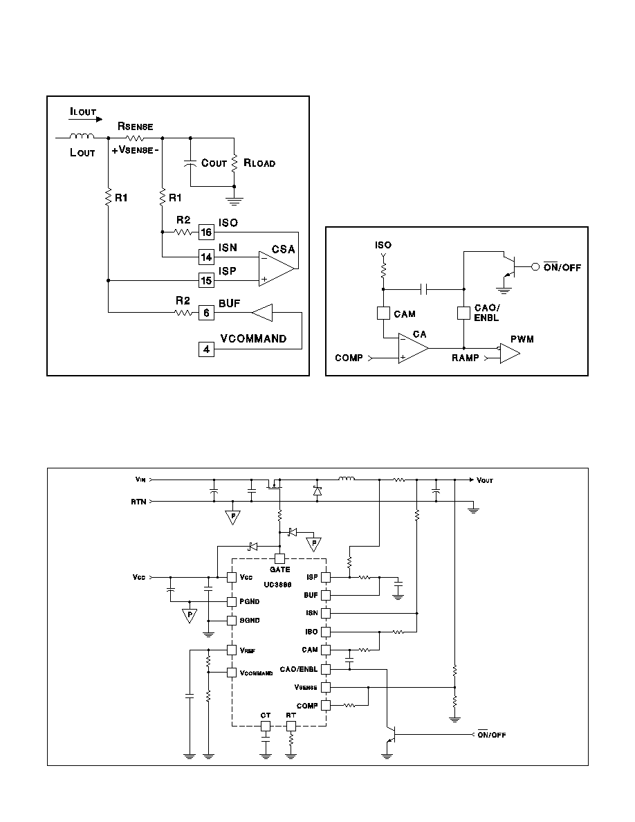
Configuring the Current Sense Amplifier
The UC3886 Current Sense Amplifier is used to amplify
a differential current sense signal across a low value
current sense resistor, R
SENSE.
This amplifier must be
set up as a differential amplifier as shown.
The Current Sense Amplifier gain, G
CSA
, is given by the
ratio of R2/R1. The output of the Current Sense Ampli-
fier at the ISO pin is given by
V
V
V
R
R
ISO
BUF
SENSE
=
+
∑
2
1
The Current Sense Amplifier gain, G
CSA
, must be pro-
grammed to be greater than or equal to 5.0 (14dB), as
this amplifier is not stable with gain below 5.0. The Cur-
rent Sense Amplifier gain is limited on the high side by
its Gain-Bandwidth product of 2.5MHz. Therefore G
CSA
must be programmed between
G
CSA_MIN
= 5.0 and
G
CSA_MAX
= 2.5MHz/F
SWITCH
APPLICATION INFORMATION
Figure 1. Oscillator
UDG-96022
0.88
0.90
0.92
0.94
0.96
0.98
1.00
0
20
40
60
80
100
120
R
T
(k
)
DMAX
Figure 2. Programming Maximum Duty Cycle with R
T
10
100
1000
0
20
40
60
80
100
RT (k
)
FSWITCH
(kHz)
100pF
220pF
470pF
1nF
Figure 3. Programming Switching Frequency with C
T
0.000
0.100
0.200
0.300
0.400
0.500
0.600
100
300
500
700
900
1100
CT (pF)
TD
(us)
RT = 5k
RT = 100k
Figure 4. Deadtime vs. C
T
and R
T
6
UC2886
UC3886
Enabling/Disabling the UC3886 Gate Drive
The CAO/ENBL pin can be used to Disable the UC3886
gate drive by forcing this pin below 0.8V, as shown.
Bringing the voltage below the valley of the PWM oscil-
lator ramp will insure a 0% duty cycle, effectively dis-
abling the gate drive. A low noise open collector signal
should be used as an Enable/Disable command.
APPLICATION INFORMATION (cont.)
Figure 5. Configuring the Current Sense Amplifier
UDG-96024
Figure 6. Enabling/Disabling the UC3886
UDG-96023
Figure 7. The UC3886 Configured in a Buck Regulator
TYPICAL APPLICATIONS
UDG-96025
7
UC2886
UC3886
UNITRODE CORPORATION
7 CONTINENTAL BLVD. ∑ MERRIMACK, NH 03054
TEL. (603) 424-2410
FAX (603) 424-3460
Figure 8. UC3886 Configured with the UC3910 for a PentiumÆ Pro DC/DC Converter
TYPICAL APPLICATIONS (cont.)
UDG-96021

IMPORTANT NOTICE
Texas Instruments and its subsidiaries (TI) reserve the right to make changes to their products or to discontinue
any product or service without notice, and advise customers to obtain the latest version of relevant information
to verify, before placing orders, that information being relied on is current and complete. All products are sold
subject to the terms and conditions of sale supplied at the time of order acknowledgment, including those
pertaining to warranty, patent infringement, and limitation of liability.
TI warrants performance of its products to the specifications applicable at the time of sale in accordance with
TI's standard warranty. Testing and other quality control techniques are utilized to the extent TI deems necessary
to support this warranty. Specific testing of all parameters of each device is not necessarily performed, except
those mandated by government requirements.
Customers are responsible for their applications using TI components.
In order to minimize risks associated with the customer's applications, adequate design and operating
safeguards must be provided by the customer to minimize inherent or procedural hazards.
TI assumes no liability for applications assistance or customer product design. TI does not warrant or represent
that any license, either express or implied, is granted under any patent right, copyright, mask work right, or other
intellectual property right of TI covering or relating to any combination, machine, or process in which such
products or services might be or are used. TI's publication of information regarding any third party's products
or services does not constitute TI's approval, license, warranty or endorsement thereof.
Reproduction of information in TI data books or data sheets is permissible only if reproduction is without
alteration and is accompanied by all associated warranties, conditions, limitations and notices. Representation
or reproduction of this information with alteration voids all warranties provided for an associated TI product or
service, is an unfair and deceptive business practice, and TI is not responsible nor liable for any such use.
Resale of TI's products or services with
statements different from or beyond the parameters stated by TI for
that product or service voids all express and any implied warranties for the associated TI product or service,
is an unfair and deceptive business practice, and TI is not responsible nor liable for any such use.
Also see: Standard Terms and Conditions of Sale for Semiconductor Products. www.ti.com/sc/docs/stdterms.htm
Mailing Address:
Texas Instruments
Post Office Box 655303
Dallas, Texas 75265
Copyright
2001, Texas Instruments Incorporated