 | –≠–ª–µ–∫—Ç—Ä–æ–Ω–Ω—ã–π –∫–æ–º–ø–æ–Ω–µ–Ω—Ç: UC3906N | –°–∫–∞—á–∞—Ç—å:  PDF PDF  ZIP ZIP |
UC2906
UC3906
application
INFO
available
Sealed Lead-Acid Battery Charger
FEATURES
∑
Optimum Control for Maximum
Battery Capacity and Life
∑
Internal State Logic Provides
Three Charge States
∑
Precision Reference Tracks
Battery Requirements Over
Temperature
∑
Controls Both Voltage and
Current at Charger Output
∑
System Interface Functions
∑
Typical Standby Supply Current
of only 1.6mA
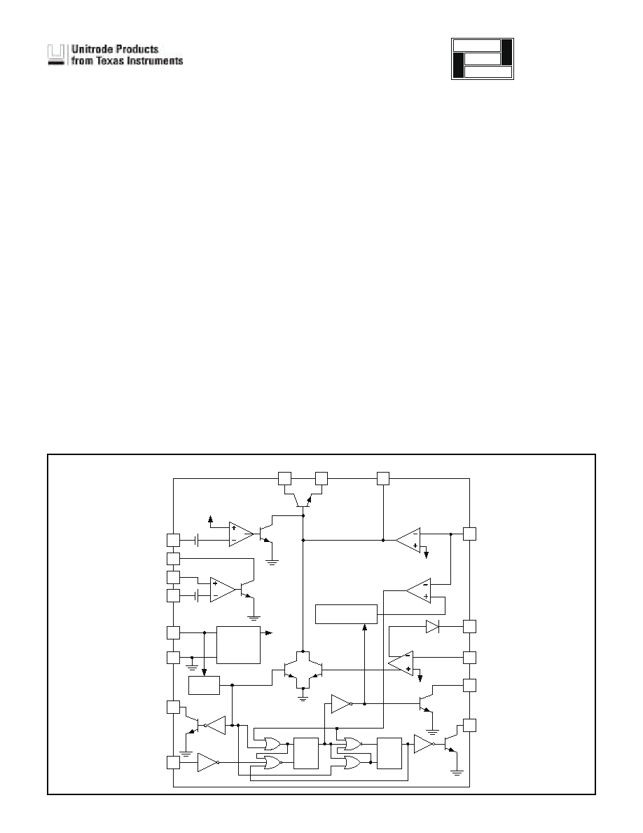
DESCRIPTION
The UC2906 series of battery charger controllers contains all of the necessary
circuitry to optimally control the charge and hold cycle for sealed lead-acid bat-
teries. These integrated circuits monitor and control both the output voltage and
current of the charger through three separate charge states; a high current
bulk-charge state, a controlled over-charge, and a precision float-charge, or
standby, state.
Optimum charging conditions are maintained over an extended temperature
range with an internal reference that tracks the nominal temperature characteris-
tics of the lead-acid cell. A typical standby supply current requirement of only
1.6mA allows these ICs to predictably monitor ambient temperatures.
Separate voltage loop and current limit amplifiers regulate the output voltage and
current levels in the charger by controlling the onboard driver. The driver will sup-
ply at least 25mA of base drive to an external pass device. Voltage and current
sense comparators are used to sense the battery condition and respond with
logic inputs to the charge state logic. A charge enable comparator with a trickle
bias output can be used to implement a low current turn-on mode of the charger,
preventing high current charging during abnormal conditions such as a shorted
battery cell.
Other features include a supply under-voltage sense circuit with a logic output to
indicate when input power is present. In addition the over-charge state of the
charger can be externally monitored and terminated using the over-charge indi-
cate output and over-charge terminate input.
+
+
4
1
3
2
5
6
7
8
16
15
14
13
S
Q
R
S
Q
R
9
10
12
11
VOLTAGE
AMPLIFIER
VREF
SENSE
COMPARATOR
VREF
VOLTAGE
SENSE
TRICKLE
BIAS
CHARGE
ENABLE
OVER-CHARGE
INDICATE
STATE LEVEL
CONTROL
OVER-CHARGE
TERMINATE
POWER
INDICATE
GND
+VIN
C/S -
C/S +
C/S OUT
C/L
L1
L2
ENABLE
COMPARATOR
VREF
DRIVER
SINK
SOURCE
COMPENSATION
HIGH 0.95 VREF
LOW 0.90 VREF
VREF 2.3 V
at -3.5 mV/C
UV
SENSE
+VIN
250 mV
25 mV
CURRENT
SENSE
CURRENT
LIMIT
BLOCK DIAGRAM
SLUS186B - SEPTEMBER 1996 - REVISED JULY 2003
2
UC2906
UC3906
ABSOLUTE MAXIMUM RATINGS
Supply Voltage (+V
IN
) . . . . . . . . . . . . . . . . . . . . . . . . . . . . . 40V
Open Collector Output Voltages . . . . . . . . . . . . . . . . . . . . . 40V
Amplifier and Comparator Input Voltages . . . . . . ≠0.3V to +40V
Over-Charge Terminate Input Voltage . . . . . . . . ≠0.3V to +40V
Current Sense Amplifier Output Current. . . . . . . . . . . . . . 80mA
Other Open Collector Output Currents . . . . . . . . . . . . . . . 20mA
Trickle Bias Voltage Differential with respect to V
IN
. . . . . ≠32V
Trickle Bias Output Current . . . . . . . . . . . . . . . . . . . . . . ≠40mA
Driver Current . . . . . . . . . . . . . . . . . . . . . . . . . . . . . . . . . . 80mA
Power Dissipation at T
A
= 25∞C (Note 2) . . . . . . . . . . . 1000mW
Power Dissipation at T
C
= 25∞C (Note 2). . . . . . . . . . . 2000mW
Operating Junction Temperature . . . . . . . . . . ≠55∞C to +150∞C
Storage Temperature . . . . . . . . . . . . . . . . . . . ≠65∞C to +150∞C
Lead Temperature (Soldering, 10 Seconds) . . . . . . . . . . 300∞C
Note 1: Voltages are referenced to ground (Pin 6). Currents
are positive into, negative out of, the specified termi-
nals.
Note 2: Consult Packaging section of Databook for thermal
limitations and considerations of packages.
DIL-16, SOIC-16 (TOP VIEW)
J or N Package, DW Package
CONNECTION DIAGRAMS
PIN FUNCTION
PIN
N/C
1
C/S OUT
2
C/S-
3
C/S+
4
C/L
5
N/C
6
+V
IN
7
GROUND
8
POWER INDICATE
9
OVER CHARGE TERMINATE 10
N/C
11
OVER CHARGE INDICATE
12
STATE LEVEL CONTROL
13
TRICKLE BIAS
14
CHARGE ENABLE
15
N/C
16
VOLTAGE SENSE
17
COMPENSATION
18
DRIVER SOURCE
19
DRIVER SINK
20
PLCC-20, LCC-20 (TOP VIEW)
Q, L Packages
ELECTRICAL CHARACTERISTICS:
Unless otherwise stated, these specifications apply for T
A
= ≠40∞C to +70∞C for the
UC2906 and 0∞C to +70∞C for the UC3906, +V
IN
= 10V, T
A
= T
J
.
PARAMETER
TEST CONDITIONS
UC2906
UC3906
UNITS
MIN
TYP
MAX
MIN
TYP
MAX
Input Supply
Supply Current
+V
IN
= 10V
1.6
3.3
1.6
3.3
mA
+V
IN
= 40V
1.8
3.6
1.8
3.6
mA
Supply Under-Voltage Threshold +V
IN
= Low to High
4.2
4.5
4.8
4.2
4.5
4.8
V
Supply Under-Voltage
Hysteresis
0.20
0.30
0.20
0.30
V
Internal Reference (V
REF
)
Voltage Level (Note 3)
Measured as Regulating Level at
Pin 13 w/ Driver Current = 1mA,
T
J
= 25∞C
2.275
2.3
2.325
2.270
2.3
2.330
V
Line Regulation
+V
IN
= 5 to 40V
3
8
3
8
mV
Temperature Coefficient
≠3.5
≠3.5
mV/∞C
3
UC2906
UC3906
ELECTRICAL CHARACTERISTICS:
Unless otherwise stated, these specifications apply for T
A
= ≠40∞C to +70∞C for the
UC2906 and 0∞C to +70∞C for the UC3906, +V
IN
= 10V, T
A
= T
J
.
PARAMETER
TEST CONDITIONS
UC2906
UC3906
UNITS
MIN
TYP
MAX
MIN
TYP
MAX
Voltage Amplifier
Input Bias Current
Total Input Bias at Regulating Level
≠0.5
≠0.2
≠0.5
≠0.2
µ
A
Maximum Output Current
Source
≠45
≠30
≠15
≠45
≠30
≠15
µ
A
Sink
30
60
90
30
60
90
µ
A
Open Loop Gain
Driver current = 1mA
50
65
50
65
dB
Output Voltage Swing
Volts above GND or below +V
IN
0.2
0.2
V
Driver
Minimum Supply to Source
Differential
Pin 16 = +V
IN
, I
O
= 10mA
2.0
2.2
2.0
2.2
V
Maximum Output Current
Pin 16 to Pin 15 = 2V
25
40
25
40
mA
Saturation Voltage
0.2
0.45
0.2
0.45
V
Current Limit Amplifier
Input Bias Current
0.2
1.0
0.2
1.0
µ
A
Threshold Voltage
Offset below +V
IN
225
250
275
225
250
275
mV
Threshold Supply Sensitivity
+V
IN
= 5 to 40V
0.03
0.25
0.03
0.25
%/V
Voltage Sense Comparator
Threshold Voltage
As a function of V
REF
, L
1
= RESET
0.94
0.949
0.960
0.94
0.949
0.960
V/V
As a function of V
REF
, L
1
= SET
0.895
0.90
0.910
0.895
0.90
0.910
V/V
Input Bias Current
Total Input Bias at Thresholds
≠0.5
≠0.2
≠0.5
≠0.2
µ
A
Current Sense Comparator
Input Bias Current
0.1
0.5
0.1
0.5
µ
A
Input Offset Current
0.01
0.2
0.01
0.2
µ
A
Input Offset Voltage
Referenced to Pin 2, I
OUT
= 1mA
20
25
30
20
25
30
mV
Offset Supply Sensitivity
+V
IN
= 5 to 40V
0.05
0.35
0.05
0.35
%/V
Offset Common Mode Sensitivity CMV = 2V to +V
IN
0.05
0.35
0.05
0.35
%/V
Maximum Output Current
V
OUT
= 2V
25
40
25
40
mA
Output Saturation Voltage
I
OUT
= 10mA
0.2
0.45
0.2
0.45
V
Enable Comparator
Threshold Voltage
As a function of V
REF
0.99
1.0
1.01
0.99
1.0
1.01
V/V
Input Bias Current
≠0.5
≠0.2
≠0.5
≠0.2
µ
A
Trickle Bias Maximum Output
Current
V
OUT
= +V
IN
-
3V
25
40
25
40
mA
Trickle Bias Maximum Output
Voltage
Volts below +V
IN
, I
OUT
= 10mA
2.0
2.6
2.0
2.6
V
Trickle Bias Reverse Hold-Off
Voltage
+V
IN
= 0V, I
OUT
= ≠10
µ
A
6.3
7.0
6.3
7.0
V
Over-Charge Terminate Input
Threshold Voltage
0.7
1.0
1.3
0.7
1.0
1.3
V
Internal Pull-Up Current
At Threshold
10
10
µ
A
Open Collector Outputs (Pins 7, 9, and 10)
Maximum Output Current
V
OUT
= 2V
2.5
5
2.5
5
mA
Saturation Voltage
I
OUT
= 1.6mA
0.25
0.45
0.25
0.45
V
I
OUT
= 50
µ
A
0.03
0.05
0.03
0.05
V
Leakage Current
V
OUT
= 40V
1
3
1
3
µ
A
Note 3. The reference voltage will change as a function of power dissipation on the die according to the temperature coefficient of
the reference and the thermal resistance, junction-to-ambient.
4
UC2906
UC3906
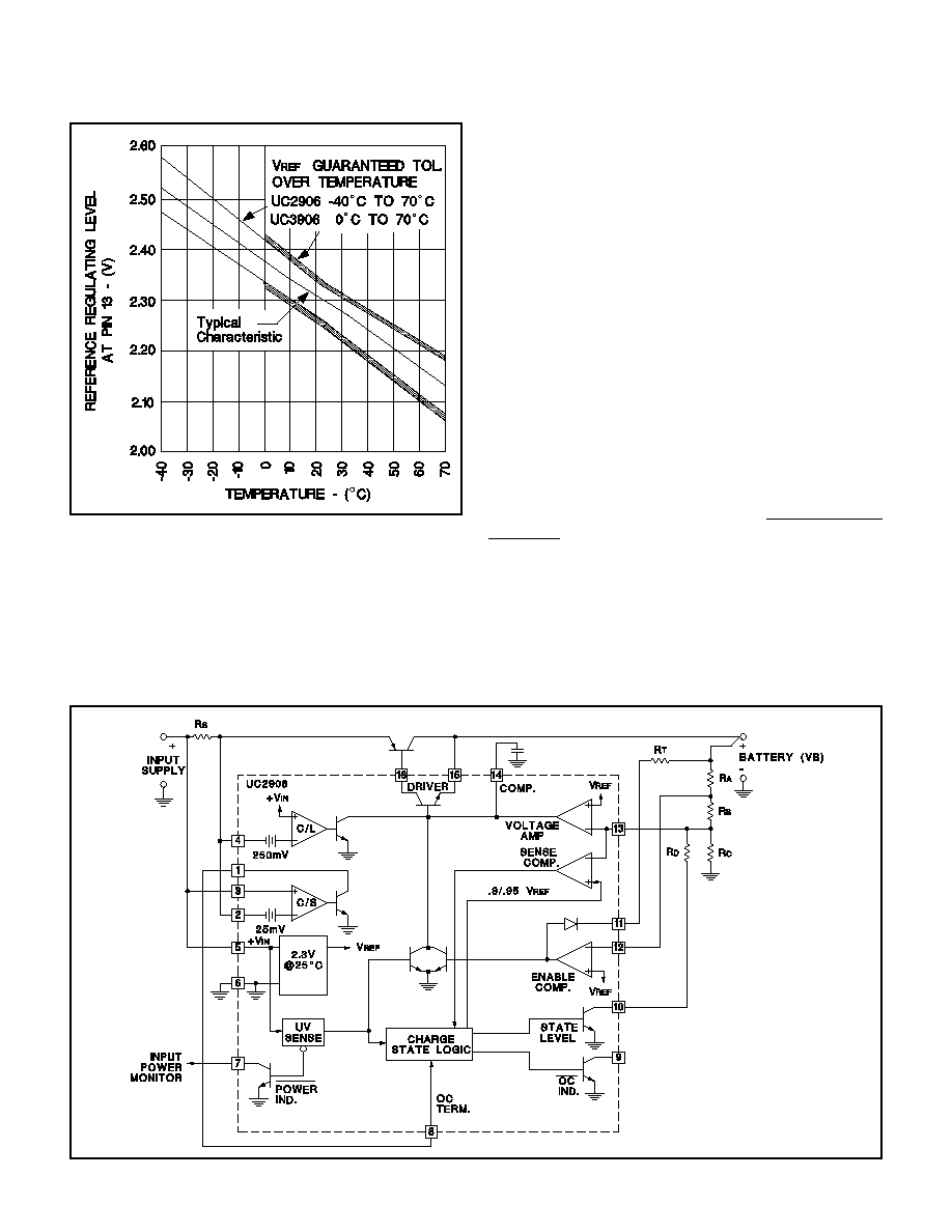
Dual Level Float Charger Operations
The UC2906 is shown configured as a dual level float
charger in Figure 1. All high currents are handled by the
external PNP pass transistor with the driver supplying
base drive to this device. This scheme uses the TRICKLE
BIAS output and the charge enable comparator to give
the charger a low current turn on mode. The output cur-
rent of the charger is limited to a low-level until the bat-
tery reaches a specified voltage, preventing a high
current charging if a battery cell is shorted. Figure 2
shows the state diagram of the charger. Upon turn on
the UV sense circuitry puts the charger in state 1, the
high rate bulk-charge state. In this state, once the enable
threshold has been exceeded, the charger will supply a
peak current that is determined by the 250mV offset in
the C/L amplifier and the sensing resistor R
S
.
To guarantee full re-charge of the battery, the charger's
voltage loop has an elevated regulating level, V
OC
, dur-
ing state 1 and state 2. When the battery voltage
reaches 95% of V
OC
, the charger enters the over-charge
state, state 2. The charger stays in this state until the
OVER-CHARGE TERMINATE pin goes high. In Figure 1,
the charger uses the current sense amplifier to generate
this signal by sensing when the charge current has ta-
pered to a specified level, I
OCT.
Alternatively the
over-charge could have been controlled by an external
source, such as a timer, by using the OVER-CHARGE
INDICATE signal at Pin 9. If a load is applied to the bat-
tery and begins to discharge it, the charger will contrib-
ute its full output to the load. If the battery drops 10%
below the float level, the charger will reset itself to state
1. When the load is removed a full charge cycle will fol-
low. A graphical representation of a charge, and dis-
charge, cycle of the dual lever float charger is shown in
Figure 3.
OPERATION AND APPLICATION INFORMATION
Figure 1. The UC2906 in a dual level float charger.
Internal reference temperature characteristic and
tolerance.
5
UC2906
UC3906
Figure 3. Typical charge cycle: UC2906 dual level float charger
.
A.
Input power turns on, battery charges at trickle current
rate.
B.
Battery voltage reaches V
T
enabling the driver and turn-
ing off the trickle bias output, battery charges at l
MAX
rate.
C.
Transition voltage V
12
is reached and the charger indi-
cates that it is now in the over-charge state, state 2.
D.
Battery voltage approaches the over-charge level V
OC
and the charge current begins to taper.
E.
Charge current tapers to l
OCT
. The current sense ampli-
fier output, in this case tied to the OC TERMINATE in-
put, goes high. The charger changes to the float state
and holds the battery voltage at V
F
.
F.
Here a load (>l
MAX
) begins to discharge the battery.
G. The load discharges the battery such that the battery
voltage falls below V
31
. The charger is now in state 1,
again.
Explanation: Dual Level Float Charger
Design Procedure
1)
Pick divider current, I
D
. Recommended value is
50 A to 100 A.
2)
R
V I
C
D
=
2 3
.
/
3)
(
)
R
R
R
V
V
I
A
B
SUM
F
D
+
=
=
≠
.
/
2 3
4)
(
)
R
V R
V
V
D
SUM
OC
F
=
∑
2 3
.
/
≠
5)
(
)(
)
(
)
R
R
R
V V
WHERE R
R
R
R
R
A
SUM
X
T
X
C
D
C
D
=
+
=
∑
+
1 2 3
≠
.
/
:
/
6)
R
R
R
B
SUM
A
=
-
7)
R
V I
S
MAX
=
0 25
.
/
8)
(
)
R
V
V
V
I
T
IN
T
T
=
≠
≠
.
/
2 5
9)
I
I
OCT
MAX
=
10
Note V
V
V
V
OC
F
:
.
,
.
,
12
31
0 95
0 90
=
=
.
For further design and application information see
UICC Application Note U-104
OPERATION AND APPLICATION INFORMATION (cont.)
Figure 2. State diagram and design equations for the dual level float charger.
6
UC2906
UC3906
Compensated Reference Matches Battery
Requirements
When the charger is in the float state, the battery will be
maintained at a precise float voltage, V
F
. The accuracy of
this float state will maximize the standby life of the battery
while the bulk-charge and over-charge states guarantee
rapid and full re-charge. All of the voltage thresholds on
the UC2906 are derived from the internal reference. This
reference has a temperature coefficient that tracks the
temperature characteristic of the optimum-charge and
hold levels for sealed lead-acid cells. This further guaran-
tees that proper charging occurs, even at temperature ex-
tremes.
Dual Step Current Charger Operation
Figures 4, 5 and 6 illustrate the UC2906's use in a differ-
ent charging scheme. The dual step current charger is
useful when a large string of series cells must be
charged. The holding-charge state maintains a slightly el-
evated voltage across the batteries with the holding cur-
rent, 1H. This will tend to guarantee equal charge
distribution between the cells. The bulk-charge state is
similar to that of the float charger with the exception that
when V
12
is reached, no over-charge state occurs since
Pin 8 is tied high at all times. The current sense amplifier
is used to regulate the holding current. In some applica-
tions a series resistor, or external buffering transistor,
may be required at the current sense output to prevent
excessive power dissipation on the UC2906.
A PNP Pass Device Reduces Minimum Input to Out-
put Differential
The configuration of the driver on the UC2906 allows a
good bit of flexibility when interfacing to an external pass
transistor. The two chargers shown in Figures 1 and 4
both use PNP pass devices, although an NPN device
driven from the source output of the UC2906 driver can
also be used. In situations where the charger must oper-
ate with low input to output differentials the PNP pass de-
vice should be configured as shown in Figure 4. The PNP
can be operated in a saturated mode with only the series
diode and sense resistor adding to the minimum differen-
tial. The series diode, D1, in many applications, can be
eliminated. This diode prevents any discharging of the
battery, except through the sensing divider, when the
charger is attached to the battery with no input supply
voltage. If discharging under this condition must be kept
to an absolute minimum, the sense divider can be refer-
enced to the POWER INDICATE pin, Pin 7, instead of
ground. In this manner the open collector off state of Pin
7 will prevent the divider resistors from discharging the
battery when the input supply is removed.
OPERATION AND APPLICATION INFORMATION (cont.)
Figure 4. The UC2906 in a dual step current charger.
7
UC2906
UC3906
A.
Input power turns on, battery charges at a rate of I
H
+
I
MAX
.
B.
Battery voltage reaches V
12
and the voltage loop
switches to the lower level V
F
. The battery is now fed with
the holding current I
H
.
C.
An external load starts to discharge the battery.
D:
When V
F
is reached the charger will supply the full cur-
rent I
MAX
+ I
H
.
E.
The discharge continues and the battery voltage reaches
V
21
causing the charger to switch back to state 1.
Explanation: Dual Step Current Charger
OPERATION AND APPLICATION INFORMATION (cont.)
Figure 5. State Diagram and design equations for the dual step current charger.
Figure 6. Typical charge cycle: UC2906 dual step current charger

IMPORTANT NOTICE
Texas Instruments Incorporated and its subsidiaries (TI) reserve the right to make corrections, modifications,
enhancements, improvements, and other changes to its products and services at any time and to discontinue
any product or service without notice. Customers should obtain the latest relevant information before placing
orders and should verify that such information is current and complete. All products are sold subject to TI's terms
and conditions of sale supplied at the time of order acknowledgment.
TI warrants performance of its hardware products to the specifications applicable at the time of sale in
accordance with TI's standard warranty. Testing and other quality control techniques are used to the extent TI
deems necessary to support this warranty. Except where mandated by government requirements, testing of all
parameters of each product is not necessarily performed.
TI assumes no liability for applications assistance or customer product design. Customers are responsible for
their products and applications using TI components. To minimize the risks associated with customer products
and applications, customers should provide adequate design and operating safeguards.
TI does not warrant or represent that any license, either express or implied, is granted under any TI patent right,
copyright, mask work right, or other TI intellectual property right relating to any combination, machine, or process
in which TI products or services are used. Information published by TI regarding third-party products or services
does not constitute a license from TI to use such products or services or a warranty or endorsement thereof.
Use of such information may require a license from a third party under the patents or other intellectual property
of the third party, or a license from TI under the patents or other intellectual property of TI.
Reproduction of information in TI data books or data sheets is permissible only if reproduction is without
alteration and is accompanied by all associated warranties, conditions, limitations, and notices. Reproduction
of this information with alteration is an unfair and deceptive business practice. TI is not responsible or liable for
such altered documentation.
Resale of TI products or services with statements different from or beyond the parameters stated by TI for that
product or service voids all express and any implied warranties for the associated TI product or service and
is an unfair and deceptive business practice. TI is not responsible or liable for any such statements.
Following are URLs where you can obtain information on other Texas Instruments products and application
solutions:
Products
Applications
Amplifiers
amplifier.ti.com
Audio
www.ti.com/audio
Data Converters
dataconverter.ti.com
Automotive
www.ti.com/automotive
DSP
dsp.ti.com
Broadband
www.ti.com/broadband
Interface
interface.ti.com
Digital Control
www.ti.com/digitalcontrol
Logic
logic.ti.com
Military
www.ti.com/military
Power Mgmt
power.ti.com
Optical Networking
www.ti.com/opticalnetwork
Microcontrollers
microcontroller.ti.com
Security
www.ti.com/security
Telephony
www.ti.com/telephony
Video & Imaging
www.ti.com/video
Wireless
www.ti.com/wireless
Mailing Address:
Texas Instruments
Post Office Box 655303 Dallas, Texas 75265
Copyright
2003, Texas Instruments Incorporated