 | –≠–ª–µ–∫—Ç—Ä–æ–Ω–Ω—ã–π –∫–æ–º–ø–æ–Ω–µ–Ω—Ç: UC3909QTR | –°–∫–∞—á–∞—Ç—å:  PDF PDF  ZIP ZIP |

UC2909
UC3909
DESCRIPTION
The UC3909 family of Switchmode Lead-Acid Battery Chargers accurately
controls lead acid battery charging with a highly efficient average current
mode control loop. This chip combines charge state logic with average cur-
rent PWM control circuitry. Charge state logic commands current or voltage
control depending on the charge state.
The chip includes undervoltage
lockout circuitry to insure sufficient supply voltage is present before output
switching starts. Additional circuit blocks include a differential current sense
amplifier, a 1.5% voltage reference, a ≠3.9mV/∞C thermistor linearization
circuit, voltage and current error amplifiers, a PWM oscillator, a PWM com-
parator, a PWM latch, charge state decode bits, and a 100mA open collec-
tor output driver.
Switchmode Lead-Acid Battery Charger
FEATURES
∑
Accurate and Efficient Control of
Battery Charging
∑
Average Current Mode Control from
Trickle to Overcharge
∑
Resistor Programmable Charge
Currents
∑
Thermistor Interface Tracks Battery
Requirements Over Temperature
∑
Output Status Bits Report on Four
Internal Charge States
∑
Undervoltage Lockout Monitors VCC
and VREF
1/99
BLOCK DIAGRAM
UDG-95007-1
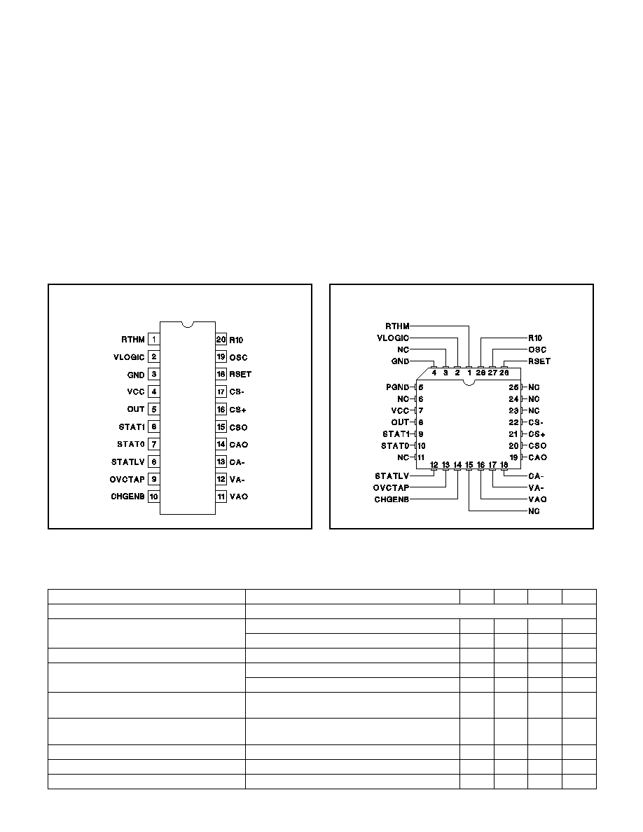
Pin numbers refer to J, N, DW packages.
2
UC2909
UC3909
DIL-20, (Top View)
J or N, DW Packages
ABSOLUTE MAXIMUM RATINGS
Supply Voltage (VCC), OUT, STAT0, STAT1 . . . . . . . . . . . 40V
Output Current Sink . . . . . . . . . . . . . . . . . . . . . . . . . . . . . . 0.1A
CS+, CS- . . . . . . . . . . . . . . . . . . . . . . . . . . -0.4 to VCC (Note 1)
Remaining Pin Voltages. . . . . . . . . . . . . . . . . . . . . . -0.3V to 9V
Storage Temperature . . . . . . . . . . . . . . . . . . . -65∞C to +150∞C
Junction Temperature . . . . . . . . . . . . . . . . . . . -55∞C to +150∞C
Lead Temperature (Soldering, 10 sec.) . . . . . . . . . . . . . +300∞C
All currents are positive into, negative out of the specified ter-
minal. Consult Packaging Section of Databook for thermal limi-
tations and considerations of packages.
Note 1: Voltages more negative than -0.4V can be tolerated if
current is limited to 50mA.
CONNECTION DIAGRAMS
ELECTRICAL CHARACTERISTICS:
Unless otherwise stated these specifications apply for T
A
= ≠40∞C to +85∞C for
UC2909; ∞0C to +70∞C for UC3909; C
T
= 330pF, R
SET
= 11.5k, R10 = 10k, R
THM
= 10k, V
CC
= 15V, Output no load, R
STAT0
=
R
STAT1
= 10k, CHGENB = OVCTAP = VLOGIC, T
A
= T
J
.
PARAMETER
TEST CONDITIONS
MIN
TYP
MAX
UNITS
Current Sense AMP (CSA) Section
V
ID
= CS+ ≠ CS≠
DC Gain
CS≠ = 0, CS+ = -50mV; CS+ = ≠250mV
4.90
5
5.10
V/V
CS+ = 0, CS≠ = 50mV; CS≠- = 250mV
4.90
5
5.10
V/V
V
OFFSET
(V
CSO
≠ V
CAO
)
CS+ = CS≠ = 2.3V, CAO = CA≠
15
mV
CMRR
V
CM
= ≠0.25 to VCC ≠ 2, 8.8 < VCC < 14
50
dB
V
CM
= ≠0.25 to VCC, 14 < VCC < 35
50
dB
V
OL
V
ID
= ≠550mV, ≠0.25V < VCM < VCC≠2,
I
O
= 500
µ
A
0.3
0.6
V
V
OH
V
ID
= +700mV, ≠0.25V < VCM < VCC≠2,
I
O
= ≠250
µ
A
5.2
5.7
6.2
V
Output Source Current
V
ID
= +700mV, CSO = 4V
≠1
≠0.5
mA
Output Sink Current
V
ID
= ≠550mV, CSO = 1V
3
4.5
mA
3dB Bandwidth
V
ID
= 90mV, V
CM
= 0V
200
kHz
LCC-28, PLCC-28 (Top View)
L, Q Packages
3
UC2909
UC3909
ELECTRICAL CHARACTERISTICS:
Unless otherwise stated these specifications apply for T
A
= ≠40∞C to +85∞C for
UC2909; ∞0C to +70∞C for UC3909; C
T
= 330pF, R
SET
= 11.5k, R10 = 10k, R
THM
= 10k, V
CC
= 15V, Output no load, R
STAT0
=
R
STAT1
= 10k, CHGENB = OVCTAP = VLOGIC, T
A
= T
J
.
PARAMETER
TEST CONDITIONS
MIN
TYP
MAX
UNITS
Current Error Amplifier (CEA) Section
I
B
8.8V < VCC < 35V, V
CHGENB
= V
LOGIC
0.1
0.8
µ
A
V
IO
(Note 2)
8.8V < VCC < 35V, CAO = CA≠
10
mV
A
VO
1V < VAO < 4V
60
90
dB
GBW
T
J
= 25∞C, F = 100kHz
1
1.5
MHz
V
OL
I
O
= 250
µ
A
0.4
0.6
V
V
OH
I
O
= ≠5mA
4.5
5
V
Output Source Current
CAO = 4V
≠25
≠12
mA
Output Sink Current
CAO = 1V
2
3
mA
I
CA
≠, I
TRCK_CONTROL
V
CHGENB
= GND
8.5
10
11.5
µ
A
Voltage Amplifier (CEA) Section
I
B
Total Bias Current; Regulating Level
0.1
1
µ
A
V
IO
(Note 2)
8.8V < VCC < 35V, VCM = 2.3V, VAO = VA≠
1.2
mV
A
VO
1V < CAO < 4V
60
90
dB
GBW
T
J
= 25∞C, F = 100kHz
0.25
0.5
MHz
V
OL
I
O
= 500
µ
A
0.4
0.6
V
V
OH
I
O
= ≠500
µ
A
4.75
5
5.25
V
Output Source Current
CAO = 4V
≠2
≠1
mA
Output Sink Current
CAO = 1V
2
2.5
mA
VAO Leakage: High Impedance State
V
CHGENB
= GND, STAT0 = 0 & STAT1 = 0,
VAO = 2.3V
≠1
1
µ
A
Pulse Width Modulator Section
Maximum Duty Cycle
CAO = 0.6V
90
95
100
%
Modulator Gain
CAO = 2.5V, 3.2V
63
71
80
%/V
OSC Peak
3
V
OSC Valley
1
V
Oscillator Section
Frequency
8.8V < VCC < 35V
198
220
242
kHz
Thermistor Derived Reference Section
V
ID
= V
RTHM
≠ V
R10
Initial Accuracy, VAO (RTHM = 10k)
V
ID
= 0, R10 = RTHM =10k (Note 3)
2.2655
2.3
2.3345
V
V
ID
= 0, R10 = RTHM =10k, ≠40∞C
T
A
< 0∞C
(Note 3)
2.254
2.3
2.346
V
Line Regulation
V
CC
= 8.8V to 35V
3
10
mV
VAO
RTHM = 138k, R10 = 10k
2.458
2.495
2.532
V
RTHM = 138k, R10 = 10k, -40∞C
T
A
< 0∞C
2.445
2.495
2.545
V
RTHM = 33.63k, R10 = 10k
2.362
2.398
2.434
V
RTHM = 33.63k, R10 = 10k, -40∞C
T
A
< 0∞C
2.350
2.398
2.446
V
RTHM = 1.014k, R10 = 10k
2.035
2.066
2.097
V
RTHM = 1.014k, R10 = 10k, -40∞C
T
A
< 0∞C
2.025
2.066
2.107
V
Charge Enable Comparator Section (CEC)
Threshold Voltage
As a function of VA≠
0.99
1
1.01
V/V
Input Bias Current
CHGENB = 2.3V
≠0.5
≠0.1
µ
A
4
UC2909
UC3909
ELECTRICAL CHARACTERISTICS:
Unless otherwise stated these specifications apply for T
A
= ≠40∞C to +85∞C for
UC2909; ∞0C to +70∞C for UC3909; C
T
= 330pF, R
SET
= 11.5k, R10 = 10k, R
THM
= 10k, V
CC
= 15V, Output no load, R
STAT0
=
R
STAT1
= 10k, CHGENB = OVCTAP = VLOGIC, T
A
= T
J
.
PARAMETER
TEST CONDITIONS
MIN
TYP
MAX
UNITS
Voltage Sense Comparator Section (VSC)
Threshold Voltage
STAT0 = 0, STAT1 = 0, Function of V
REF
0.945
0.95
0.955
V/V
STAT0 = 1, STAT1 = 0, Function of V
REF
0.895
0.9
0.905
V/V
Over Charge Taper Current Comparator Section (OCTIC)
Threshold Voltage
Function of 2.3V REF, CA- = CAO
0.99
1
1.01
V/V
Input Bias Current
OVCTAP = 2.3V
≠0.5
≠0.1
µ
A
Logic 5V Reference Section (VLOGIC)
VLOGIC
VCC = 15V
4.875
5.0
5.125
V
Line Regulation
8.8V < V
CC
< 35V
3
15
mV
Load Regulation
0 < I
O
< 10mA
3
15
mV
Reference Comparator Turn-on Threshold
4.3
4.8
V
Short Circuit Current
V
REF
= 0V
30
50
80
mA
Output Stage Section
I
SINK
Continuous
50
mA
I
PEAK
100
mA
V
OL
I
O
=50mA
1
1.3
V
Leakage Current
V
OUT
=35V
25
µ
A
STAT0 & STAT1 Open Collector Outputs Section
Maximum Sink Current
V
OUT
= 8.8V
6
10
mA
Saturation Voltage
I
OUT
= 5mA
0.1
0.45
V
Leakage Current
V
OUT
= 35V
25
µ
A
STATLV Open Collector Outputs Section
Maximum Sink Current
V
OUT
= 5V
2.5
5
mA
Saturation Voltage
I
OUT
= 2mA
0.1
0.45
V
Leakage current
V
OUT
= 5V
3
µ
A
UVLO Section
Turn-on Threshold
6.8
7.8
8.8
V
Hysteresis
100
300
500
mV
I
CC
Section
I
CC
(run)
(See Fig. 1)
13
19
mA
I
CC
(off)
VCC = 6.5V
2
mA
Note 2: VIO is measured prior to packaging with internal probe pad.
Note 3: Thermistor initial accuracy is measured and trimmed with respect to VAO; VAO = VA≠.
CA≠: The inverting input to the current error amplifier.
CAO: The output of the current error amplifier which is
internally clamped to approximately 4V. It is internally
connected to the inverting input of the PWM comparator.
CS≠, CS+: The inverting and non-inverting inputs to the
current sense amplifier. This amplifier has a fixed gain of
five and a common-mode voltage range of from ≠250mV
to +VCC.
CSO: The output of the current sense amplifier which is
internally clamped to approximately 5.7V.
CHGENB: The input to a comparator that detects when
battery voltage is low and places the charger in a trickle
charge state. The charge enable comparator makes the
output of the voltage error amplifier a high impedance
while forcing a fixed 10
µ
A into CA≠ to set the trickle
charge current.
PIN DESCRIPTIONS
5
UC2909
UC3909
GND: The reference point for the internal reference, all
thresholds, and the return for the remainder of the de-
vice. The output sink transistor is wired directly to this
pin.
OVCTAP: The overcharge current taper pin detects
when the output current has tapered to the float thresh-
old in the overcharge state.
OSC: The oscillator ramp pin which has a capacitor (C
T
)
to ground. The ramp oscillates between approximately
1.0V to 3.0V and the frequency is approximated by:
frequency
C
R
T
SET
=
∑
∑
1
1 2
.
OUT: The output of the PWM driver which consists of an
open collector output transistor with 100mA sink capabil-
ity.
R10: Input used to establish a differential voltage corre-
sponding to the temperature of the thermistor. Connect
a 10k resistor to ground from this point.
RSET:
A resistor to ground programs the oscillator
charge current and the trickle control current for the oscil-
lator ramp.
The oscillator charge current is approximately
1 75
.
R
SET
.
The trickle control current (I
TRCK_CONTROL
) is approxi-
mately
0115
.
R
SET
.
RTHM: A 10k thermistor is connected to ground and is
thermally connected to the battery. The resistance will
vary exponentially over temperature and its change is
used to vary the internal 2.3V reference by ≠3.9mV/∞C.
The recommended thermistor for this function is part
number L1005-5744-103-D1, Keystone Carbon Com-
pany, St. Marys, PA.
STAT0:
This open collector pin is the first decode bit
used to decode the charge states.
STAT1: This open collector pin is the second decode bit
used to decode the charge states.
STATLV: This bit is high when the charger is in the float
state.
VA≠: The inverting input to the voltage error amplifier.
VAO: The output of the voltage error amplifier. The up-
per output clamp voltage of this amplifier is 5V.
VCC: The input voltage to the chip. The chip is opera-
tional between 7.5V and 40V and should be bypassed
with a 1
µ
F capacitor. A typical I
CC
vs. temperature is
shown in Figure 1.
VLOGIC: The precision reference voltage. It should be
bypassed with a 0.1
µ
F capacitor.
Charge State Decode Chart
STAT0 and STAT1 are open collector outputs. The out-
put is approximately 0.2V for a logic 0.
STAT1
STAT0
Trickle Charge
0
0
Bulk Charge
0
1
Over Charge
1
0
Float Charge
1
1
PIN DESCRIPTIONS (cont.)
Figure 1. I
CC
vs. temperature.

6
UC2909
UC3909
APPLICATION INFORMATION
A Block Diagram of the UC3909 is shown on the first
page, while a Typical Application Circuit is shown in Fig-
ure 2. The circuit in Figure 2 requires a DC input voltage
between 12V and 40V.
The UC3909 uses a voltage control loop with average
current limiting to precisely control the charge rate of a
lead-acid battery.
The small increase in complexity of
average current limiting is offset by the relative simplicity
of the control loop design.
CONTROL LOOP
Current Sense Amplifier
This amplifier measures the voltage across the sense re-
sistor RS with a fixed gain of five and an offset voltage of
2.3V. This voltage is proportional to the battery current.
The most positive voltage end of RS is connected to CS-
ensuring the correct polarity going into the PWM com-
parator.
CSO = 2.3V when there is zero battery current.
RS is chosen by dividing 350mV by the maximum allow-
able load current. A smaller value for RS can be chosen
to reduce power dissipation.
Maximum Charge Current, Ibulk, is set by knowing the
maximum voltage error amplifier output, V
OH
= 5V, the
maximum allowable drop across RS, and setting the re-
sistors RG1 and RG2 such that;
(1)
RG
RG
V
VLOGIC
CA
V
V
V
V
V
RS
RS
RS
1
2
5
5
5
2 3
5
2 7
1 85
=
∑
=
∑
=
∑
=
≠
≠
≠ .
.
.
2
∑
∑
I
RS
BULK
The maximum allowable drop across RS is specified to
limit the maximum swing at CSO to approximately 2.0V
to keep the CSO amplifier output from saturating.
No charge/load current: V
CSO
= 2.3V,
Max charge/load current: V
max(CSO)
= 2.3V≠2.0V = 0.3V
Voltage Error Amplifier:
The voltage error amplifier (VEA) senses the battery
voltage and compares it to the 2.3V ≠ 3.9mV/∞C thermis-
tor generated reference. Its output becomes the current
command signal and is summed with the current sense
amplifier output. A 5.0V voltage error amplifier upper
clamp limits maximum load current. During the trickle
charge state, the voltage amplifier output is opened (high
impedance output) by the charge enable comparator. A
trickle bias current is summed into the CA≠ input which
sets the maximum trickle charge current.
The VEA, V
OH
= 5V clamp saturates the voltage loop
and consequently limits the charge current as stated in
Equation 1.
During the trickle bias state the maximum allowable
charge current (ITC) is similarly determined:
(2)
ITC
I
RG
RS
TRICK CONTROL
=
∑
∑
_
1
5
I
TRCK_CONTROL
is the fixed control current into CA≠.
I
TRCK_CONTROL
is 10
µ
A when R
SET
= 11.5k. See RSET
pin description for equation.
Current Error Amplifier
The current error amplifier (CA) compares the output of
the current sense amplifier to the output of the voltage
error amplifier. The output of the CA forces a PWM duty
cycle which results in the correct average battery current.
With integral compensation, the CA will have a very high
DC current gain, resulting in effectively no average DC
current error. For stability purposes, the high frequency
gain of the CA must be designed such that the magni-
tude of the down slope of the CA output signal is less
than or equal to the magnitude of the up slope of the
PWM ramp.
CHARGE ALGORITHM
Refer to Figure 3 in UC3906 Data Sheet in the data
book.
A) Trickle Charge State
STAT0 = STAT1 = STATLV = logic 0
When CHGNB is less than VREF (2.3V ≠ 3.9mV/∞C),
STATLV is forced low. This decreases the sense voltage
divider ratio, forcing the battery to overcharge (VOC).
(3)
(
)
VOC
VREF
RS
RS
RS
RS
RS
RS
=
∑
+
+
(
)
(
)
||
1
2
3
4
3
4
| |
During the trickle charge state, the output of the voltage
error amplifier is high impedance. The trickle control cur-
rent is directed into the CA≠ pin setting the maximum
trickle charge current. The trickle charge current is de-
fined in Equation 2.
B) Bulk Charge State
STAT1 = STATLV = logic 0, STAT0 = logic 1
As the battery charges, the UC3909 will transition from
trickle to bulk charge when CHGENB becomes greater
than 2.3V. The transition equation is
(4)
VT VREF
RS
RS
RS
RS
RS
RS
RS
=
∑
+
+
+
(
||
)
(
||
)
1
2
3
4
2
3
4
STATLV is still driven low.

7
UC2909
UC3909
UDG-95008-1
APPLICATION INFORMATION (cont.)
Figure 2. Typical application circuit
Pin
numbers
refer
to
J,
N,
DW
packages.

8
UC2909
UC3909
During the bulk charge state, the voltage error amplifier
is now operational and is commanding maximum charge
current (I
BULK
) set by Equation 1. The voltage loop at-
tempts to force the battery to VOC.
C) Overcharge State
STAT0 = STATLV = logic 0, STAT1 = logic 1
The battery voltage surpasses 95% of VOC indicating
the UC3909 is in its overcharge state.
During the overcharge charge state, the voltage loop be-
comes stable and the charge current begins to taper off.
As the charge current tapers off, the voltage at CSO in-
creases toward its null point of 2.3V. The center connec-
tion of the two resistors between CSO and VLOGIC sets
the overcurrent taper threshold (OVCTAP). Knowing the
desired overcharge terminate current (I
OCT
), the resistors
R
OVC1
and R
OVC2
can be calculated by choosing a value
of R
OVC2
and using the following equation:
(5)
(
)
R
I
RS
R
OVC
OCT
OVC
1
2
18518
=
∑
∑
∑
.
D) Float State
STAT0 = STAT1 = STATLV = logic 1
The battery charge current tapers below its OVCTAP
threshold, and forces STATLV high increasing the volt-
age sense divider ratio. The voltage loop now forces the
battery charger to regulate at its float state voltage (V
F
).
(6)
(
)
(
)
V
V
RS
RS
RS
RS
F
REF
=
+
+
1
2
3
3
If the load drains the battery to less than 90% of V
F
, the
charger goes back to the bulk charge state, STATE 1.
OFF LINE APPLICATIONS
For off line charge applications, either Figure 3 or Figure
4 can be used as a baseline. Figure 3 has the advan-
tage of high frequency operation resulting in a small iso-
lation transformer. Figure 4 is a simpler design, but at
the expense of larger magnetics.
APPLICATION INFORMATION (cont.)
Figure 3. Off line charger with primary side PWM
UDG-95009

9
UC2909
UC3909
Figure 4. Isolated off line charger
APPLICATION INFORMATION (cont.)
UNITRODE CORPORATION
7 CONTINENTAL BLVD. ∑ MERRIMACK, NH 03054
TEL. (603) 424-2410 ∑ FAX (603) 424-3460
UDG-95010

IMPORTANT NOTICE
Texas Instruments and its subsidiaries (TI) reserve the right to make changes to their products or to discontinue
any product or service without notice, and advise customers to obtain the latest version of relevant information
to verify, before placing orders, that information being relied on is current and complete. All products are sold
subject to the terms and conditions of sale supplied at the time of order acknowledgement, including those
pertaining to warranty, patent infringement, and limitation of liability.
TI warrants performance of its semiconductor products to the specifications applicable at the time of sale in
accordance with TI's standard warranty. Testing and other quality control techniques are utilized to the extent
TI deems necessary to support this warranty. Specific testing of all parameters of each device is not necessarily
performed, except those mandated by government requirements.
CERTAIN APPLICATIONS USING SEMICONDUCTOR PRODUCTS MAY INVOLVE POTENTIAL RISKS OF
DEATH, PERSONAL INJURY, OR SEVERE PROPERTY OR ENVIRONMENTAL DAMAGE ("CRITICAL
APPLICATIONS"). TI SEMICONDUCTOR PRODUCTS ARE NOT DESIGNED, AUTHORIZED, OR
WARRANTED TO BE SUITABLE FOR USE IN LIFE-SUPPORT DEVICES OR SYSTEMS OR OTHER
CRITICAL APPLICATIONS. INCLUSION OF TI PRODUCTS IN SUCH APPLICATIONS IS UNDERSTOOD TO
BE FULLY AT THE CUSTOMER'S RISK.
In order to minimize risks associated with the customer's applications, adequate design and operating
safeguards must be provided by the customer to minimize inherent or procedural hazards.
TI assumes no liability for applications assistance or customer product design. TI does not warrant or represent
that any license, either express or implied, is granted under any patent right, copyright, mask work right, or other
intellectual property right of TI covering or relating to any combination, machine, or process in which such
semiconductor products or services might be or are used. TI's publication of information regarding any third
party's products or services does not constitute TI's approval, warranty or endorsement thereof.
Copyright
©
1999, Texas Instruments Incorporated