 | –≠–ª–µ–∫—Ç—Ä–æ–Ω–Ω—ã–π –∫–æ–º–ø–æ–Ω–µ–Ω—Ç: UC39432 | –°–∫–∞—á–∞—Ç—å:  PDF PDF  ZIP ZIP |
UC19432
UC29432
UC39432
UC39432B
DESCRIPTION
The UC39432 is an adjustable precision analog controller with 100mA sink
capability if the ISET pin is grounded. A resistor between ISET and ground
will modify the transconductance while decreasing the maximum current
sink. This will add further control in the optocoupler configuration. The
trimmed precision reference along with the non-inverting error amplifier in-
puts are accessible for custom configuration. A sister device, the UC39431
adjustable shunt regulator, has an on-board resistor network providing six
preprogrammed voltage levels, as well as external programming capability.
Precision Analog Controller
FEATURES
∑
Programmable Transconductance for
Optimum Current Drive
∑
Accessible 1.3V Precision Reference
∑
Both Error Amplifier Inputs Available
∑
0.7% Overall Reference Tolerance
∑
0.4% Initial Accuracy
∑
2.2V to 36.0V Operating Supply
Voltage and User Programmable
Reference
∑
Reference Accuracy Maintained for
Entire Range of Supply Voltage
∑
Superior Accuracy and Easier
Compensation for Optoisolator
Application
∑
Low Quiescent Current (0.50mA Typ)
03/99
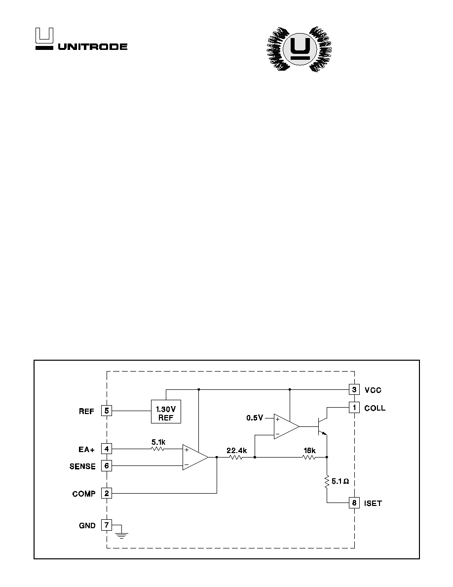
BLOCK DIAGRAM
UDG-95093
2
UC19432
UC29432
UC39432
UC39432B
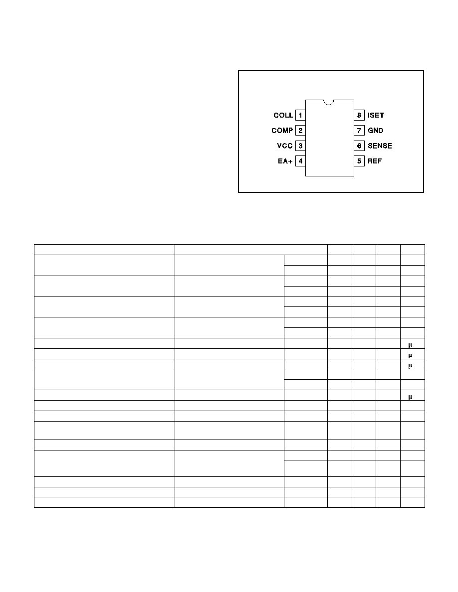
DIL-8, SOIC-8 (Top View)
N or J, D Package
ABSOLUTE MAXIMUM RATINGS
Supply Voltage: VCC . . . . . . . . . . . . . . . . . . . . . . . . . . . . . . 36V
Regulated Output: V
COLL
. . . . . . . . . . . . . . . . . . . . . . . . . . . 36V
EA Input: SENSE, EA+ . . . . . . . . . . . . . . . . . . . . . . . . . . . . . 6V
EA Compensation: COMP . . . . . . . . . . . . . . . . . . . . . . . . . . . 6V
Reference Output: REF . . . . . . . . . . . . . . . . . . . . . . . . . . . . . 6V
Output Sink Current: I
COLL
. . . . . . . . . . . . . . . . . . . . . . . 140mA
Output Source Current: ISET . . . . . . . . . . . . . . . . . . . . ≠140mA
Power Dissipation at T
A
25∞C (DIL-8) . . . . . . . . . . . . . . . . 1W
Derate 8mW/∞C for T
A
> 25∞C
Storage Temperature Range . . . . . . . . . . . . . ≠65∞C to +150∞C
Junction Temperature . . . . . . . . . . . . . . . . . . . ≠55∞C to +150∞C
Lead Temperature (Soldering, 10 sec.) . . . . . . . . . . . . . +300∞C
Currents are positive into, negative out of the specified termi-
nal. Consult Packaging Section of Databook for thermal limita-
tions and considerations of packages.
ELECTRICAL CHARACTERISTICS:
Unless otherwise stated, these specifications apply for T
A
= ≠55∞C to +125∞C and
COLL Output = 2.4V to 36.0V for the UC19432, T
A
= ≠25∞C to +85∞C and COLL Output = 2.3V to 36.0V for the UC29432, and T
A
= 0∞C to +70∞C and COLL Output = 2.3V to 36.0V for the UC39432, VCC = 15V, I
COLL
= 10mA, T
A
= T
J
.
PARAMETER
TEST CONDITIONS
MIN
TYP
MAX
UNITS
Reference Voltage Tolerance
T
A
= 25∞C
19432*
1.295
1.3
1.305
V
39432B
1.29
1.3
1.31
V
Reference Temperature Tolerance
V
COLL
= 5.0V
19432*
1.291
1.3
1.309
V
39432B
1.286
1.3
1.314
V
Reference Line Regulation
VCC = 2.4V to 36.0V, V
COLL
= 5V
19432*
10
38
mV
39432B
10
57
mV
Reference Load Regulation
I
COLL
= 10mA to 50mA, V
COLL
= 5V
19432*
10
38
mV
39432B
10
57
mV
Reference Sink Current
10
A
Reference Source Current
≠10
A
EA Input Bias Current
≠0.5
≠0.2
A
EA Input Offset Voltage
19432*
4.0
mV
39432B
4.0
mV
EA Output Current Sink (Internally Limited)
16
A
EA Output Current Source
≠1
mA
Minimum Operating Current
VCC = 36.0V, V
COLL
= 5V
0.50
0.80
mA
Collector Current Limit (Note)
V
COLL
= VCC = 36.0V, Ref = 1.35V
ISET = GND
130
145
mA
Collector Saturation
I
COLL
= 20mA
0.7
1.1
1.5
V
Transconductance (gm) (Note)
VCC = 2.4V to 36.0V,
V
COL
= 3V, I
COLL
= 20mA
ISET = GND
19432*
≠170
≠140
≠110
mS
39432B
≠180
≠140
≠100
mS
Error Amplifier AVOL
60
90
dB
Error Amplifier GBW
(Note 1)
3.0
5
MHz
Transconductance Amplifier GBW
3
MHz
* Also applies to the UC29432 and UC39432
Note:
Programmed transconductance and collector current limit equations are specified in the ISET pin description.
Note 1: Guaranteed by design. Not 100% tested in production.
CONNECTION DIAGRAM
3
UC19432
UC29432
UC39432
UC39432B
COLL: The collector of the output transistor with a maxi-
mum voltage of 36V. This pin is the output of the
transconductance amplifier. The overall open loop volt-
age gain of the transconductance amplifier is gm ∑ R
L
,
where gm is designed to be ≠140mS ±30mS and RL rep-
resents the output load.
COMP: The output of the error amplifier and the input to
the transconductance amplifier. This pin is available to
compensate the high frequency gain of the error ampli-
fier. It is internally voltage limited to approximately 2.0V.
EA+: The non-inverting input to the error amplifier.
GND: The reference and power ground for the device.
The power ground of the output transistor is isolated on
the chip from the substrate ground used to bias the re-
mainder of the device.
ISET: The current set pin for the transconductance ampli-
fier. The transconductance will be ≠140mS as specified
in the electrical table if this pin is grounded. If a resis-
tance R
L
is added to the ISET pin, the resulting new
transconductance is calculated using the following equa-
tion: gm = ≠0.714V
∑
(5.1
+ R
L
). The maximum current
will be approximately
I
V
R
MAX
L
=
+
0 6
5 1
.
.
REF: The output of the trimmed precision reference. It
can source or sink 10 A and still maintain the 1% tem-
perature specification.
SENSE: The inverting terminal of the error amplifier used
as both the voltage sense input to the error amplifier and
its other compensation point. The error amplifier uses the
SENSE input to compare against the 1.3V on-chip refer-
ence.
The SENSE pin is also used as the undervoltage lockout
(UVLO). It is intended to keep the chip from operating un-
til the internal reference is properly biased. The threshold
is approximately 1V. It is important that once the UVLO is
released,
the
error
amplifier
can
drive
the
transconductance amplifier to stabilize the loop. If a ca-
pacitor is connected between the SENSE and COMP
pins to create a pole, it will limit the slew rate of the error
amplifier. To increase the bandwidth and ensure startup
at low load current, it is recommended to create a zero
along with the pole as shown in the UC39431 shunt reg-
ulator application. The error amplifier must slew 2.0V to
drive the transconductance amplifier initially on.
VCC: The power connection for the device. The minimum
to maximum operating voltage is 2.2V to 36.0V. The qui-
escent current is typically 0.50mA.
PIN DESCRIPTIONS
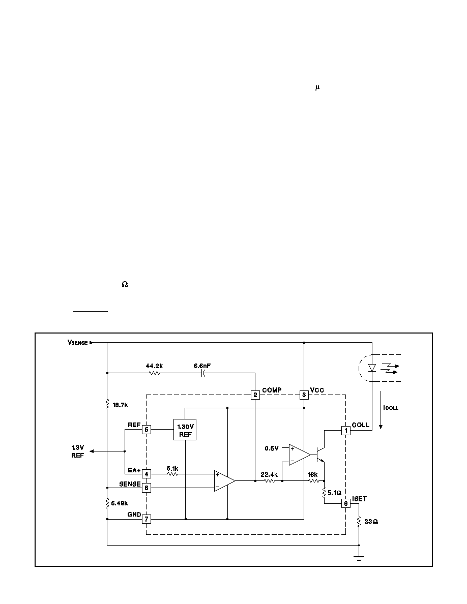
Figure 1. 5.0V Optocoupler application.
UDG-95094
4
UC19432
UC29432
UC39432
UC39432B
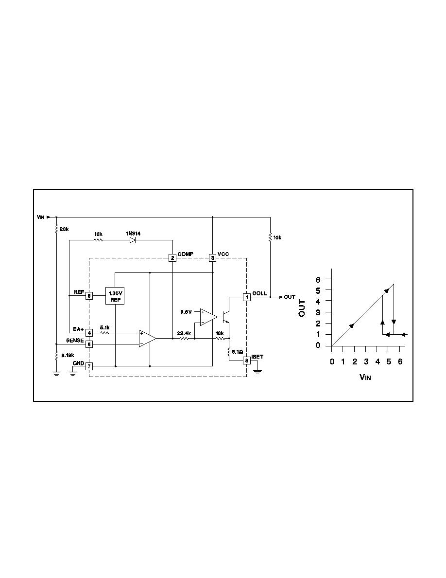
OVERVOLTAGE COMPARATOR APPLICATION
The signal V
IN
senses the input voltage. As long as the
input voltage is less than 5.5V, the output is equal to the
voltage on V
IN
. During this region of operation, the diode
is reversed biased which keeps the EA+ pin at 1.3V.
When V
IN
exceeds the over voltage threshold of 5.5V, the
output is driven low. This forward biases the diode and
creates hysteresis by changing the threshold to 4.5V.
OPTOCOUPLER APPLICATION
The optocoupler application shown takes advantage of
the accessible pins REF and ISET. The ISET pin has a
33 ohm resistor to ground that protects the opto-coupler
by limiting the current to about 16mA. This also lowers
the transconductance to approximately 19mS. The ability
to adjust the transconductance gives the designer further
control of the loop gain. The REF pin is available to sat-
isfy any high precision voltage requirements.
Figure 2. 5.5V Overvoltage comparator with hysteresis.
UDG-95096
UDG-95095
UNITRODE CORPORATION
7 CONTINENTAL BLVD. ∑ MERRIMACK, NH 03054
TEL. (603) 424-2410 ∑ FAX (603) 424-3460

IMPORTANT NOTICE
Texas Instruments and its subsidiaries (TI) reserve the right to make changes to their products or to discontinue
any product or service without notice, and advise customers to obtain the latest version of relevant information
to verify, before placing orders, that information being relied on is current and complete. All products are sold
subject to the terms and conditions of sale supplied at the time of order acknowledgement, including those
pertaining to warranty, patent infringement, and limitation of liability.
TI warrants performance of its semiconductor products to the specifications applicable at the time of sale in
accordance with TI's standard warranty. Testing and other quality control techniques are utilized to the extent
TI deems necessary to support this warranty. Specific testing of all parameters of each device is not necessarily
performed, except those mandated by government requirements.
CERTAIN APPLICATIONS USING SEMICONDUCTOR PRODUCTS MAY INVOLVE POTENTIAL RISKS OF
DEATH, PERSONAL INJURY, OR SEVERE PROPERTY OR ENVIRONMENTAL DAMAGE ("CRITICAL
APPLICATIONS"). TI SEMICONDUCTOR PRODUCTS ARE NOT DESIGNED, AUTHORIZED, OR
WARRANTED TO BE SUITABLE FOR USE IN LIFE-SUPPORT DEVICES OR SYSTEMS OR OTHER
CRITICAL APPLICATIONS. INCLUSION OF TI PRODUCTS IN SUCH APPLICATIONS IS UNDERSTOOD TO
BE FULLY AT THE CUSTOMER'S RISK.
In order to minimize risks associated with the customer's applications, adequate design and operating
safeguards must be provided by the customer to minimize inherent or procedural hazards.
TI assumes no liability for applications assistance or customer product design. TI does not warrant or represent
that any license, either express or implied, is granted under any patent right, copyright, mask work right, or other
intellectual property right of TI covering or relating to any combination, machine, or process in which such
semiconductor products or services might be or are used. TI's publication of information regarding any third
party's products or services does not constitute TI's approval, warranty or endorsement thereof.
Copyright
©
1999, Texas Instruments Incorporated