 | –≠–ª–µ–∫—Ç—Ä–æ–Ω–Ω—ã–π –∫–æ–º–ø–æ–Ω–µ–Ω—Ç: UC495AC | –°–∫–∞—á–∞—Ç—å:  PDF PDF  ZIP ZIP |

Advanced Regulating Pulse Width Modulators
FEATURES
∑
Dual Uncommitted 40V, 200mA
Output Transistors
∑
1% Accurate 5V Reference
∑
Dual Error Amplifiers
∑
Wide Range, Variable Deadtime
∑
Single-ended or Push-pull
Operation
∑
Under-voltage Lockout With
Hysteresis
∑
Double Pulse Protection
∑
Master or Slave Oscillator
Operation
∑
UC495A: Internal 39V Zener Diode
∑
UC495A: Buffered Steering Control
DESCRIPTION
This entire series of PWM modulators each provide a complete pulse width
modulation system in a single monolithic integrated circuit. These devices in-
clude a 5V reference accurate to
±
1%, two independent amplifiers usable for
both voltage and current sensing, an externally synchronizable oscillator
with its linear ramp generator, and two uncommitted transistor output
switches. These two outputs may be operated either in parallel for single-
ended operation or alternating for push-pull applications with an externally
controlled dead-band. These units are internally protected against double-
pulsing of a single output or from extraneous output signals when the input
supply voltage is below minimum.
The UC495A contains an on-chip 39V zener diode for high-voltage applica-
tions where V
CC
would be greater than 40V, and a buffered output steering
control that overrides the internal control of the pulse steering flip-flop.
The UC494A is packaged in a 16-pin DIP, while the UC495A is packaged in
an 18 pin DIP. The UC494A, UC495A are specified for operation over the full
military temperature range of -55∞C to +125∞C, while the UC494AC,
UC495AC are designed for industrial applications from 0∞C to +70∞C.
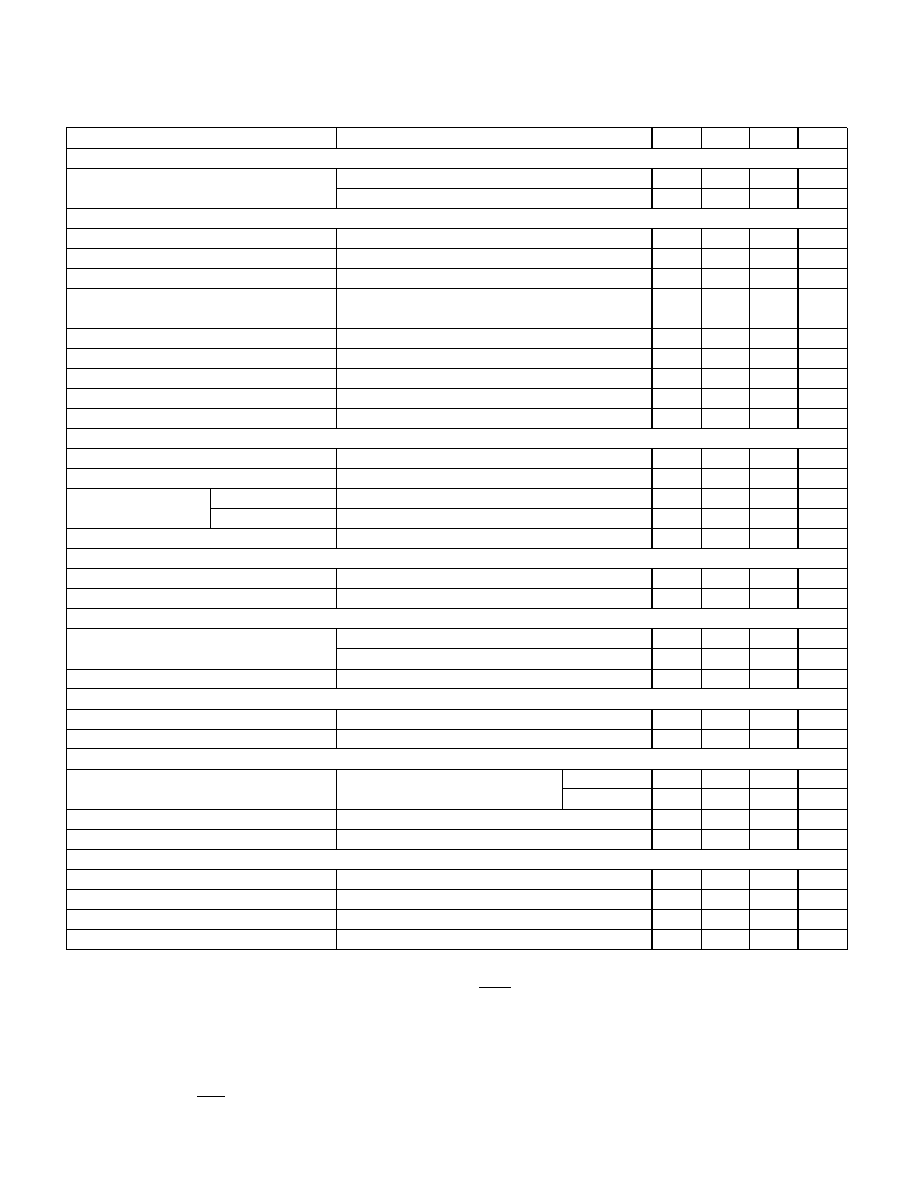
BLOCK DIAGRAM
UC494A/AC
UC495A/AC
10/93
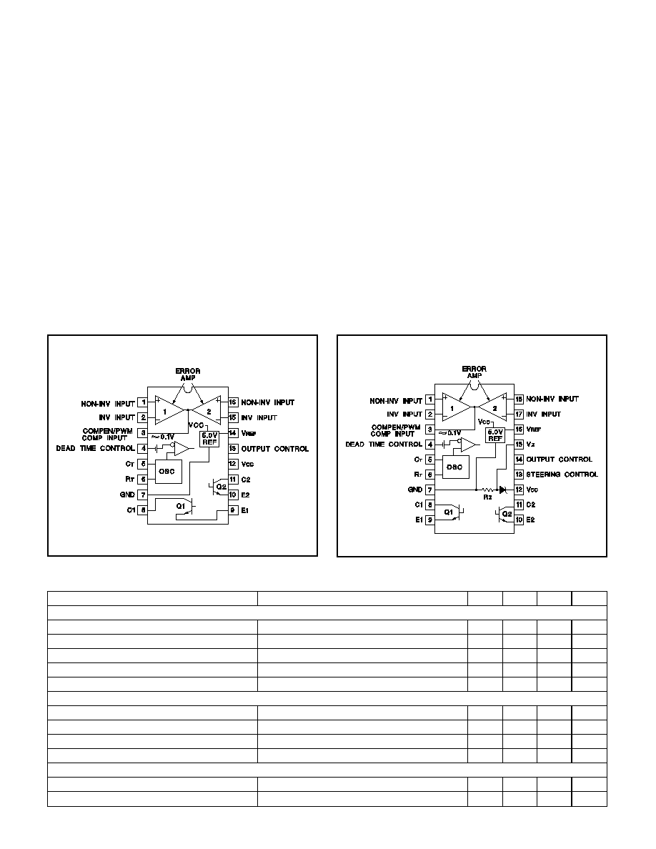
CONNECTION DIAGRAMS
DIL-18 (TOP VIEW)
J or N Package
DIL-18 (TOP VIEW)
J or N Package
UC494A/AC
UC495A/AC
ABSOLUTE MAXIMUM RATINGS (Note 1, 2, 3)
Supply Voltage, V
CC
(Note 2). . . . . . . . . . . . . . . . . . . . . . . . 45V
Amplifier Input Voltages . . . . . . . . . . . . . . . . . . . . . . V
CC
+ 0.3V
Collector Output Voltage . . . . . . . . . . . . . . . . . . . . . . . . . . . 41V
Collector Output Current. . . . . . . . . . . . . . . . . . . . . . . . . 250mA
Continuous Total Dissipation . . . . . . . . . . . . . . . . . . . . 1000mW
@ (or below) 25
∞
C free air temperature range (Note 3)
Storage Temperature Range . . . . . . . . . . . . . . . -65∞ to +150∞C
Lead Temperature 1/16" (1.6mm) from case for 60 seconds,
J Package . . . . . . . . . . . . . . . . . . . . . . . . . . . . . . . . . . . 300∞C
Lead Temperature 1/16" (1.6mm) from case for 10 seconds,
N Package . . . . . . . . . . . . . . . . . . . . . . . . . . . . . . . . . . 260∞C
Note 1: Over operating free air temperature range unless
otherwise noted.
Note 2: All voltage values are with respect to network
ground terminal 3.
Note 3: Consult Packaging Section of Databook regarding
thermal specifications and limitations of packages.
RECOMMENDED OPERATING CONDITIONS
Supply Voltage V
CC
. . . . . . . . . . . . . . . . . . . . . . . . . . 7V to 40V
Error Amplifier Input Voltages . . . . . . . . . . . . . -0.3V to V
CC
-2V
Collector Output Voltage . . . . . . . . . . . . . . . . . . . . . . . . . . . 40V
Collector Output Current (each transistor) . . . . . . . . . . . 200mA
Current into Feedback Terminal. . . . . . . . . . . . . . . . . . . . 0.3mA
Timing Capacitor, C
T
. . . . . . . . . . . . . . . . . 0.47nF to 10,000nF
Timing Resistor, R
T
. . . . . . . . . . . . . . . . . . . . . 1.8k
to 500k
Oscillator Frequency . . . . . . . . . . . . . . . . . . . . 1kHz to 300kHz
Operating Free Air Temperature
UC494A, UC495A . . . . . . . . . . . . . . . . . . . . -55∞C to +125∞C
UC494AC, UC495AC . . . . . . . . . . . . . . . . . . . . 0∞C to +70∞C
ELECTRICAL CHARACTERISTICS:
PARAMETER
TEST CONDITIONS
MIN
TYP
MAX
UNITS
Reference Section
Output Voltage V
REF
I
O
= 1mA, T
A
= 25
∞
C
4.95
5
5.05
V
Input Regulation
V
CC
= 7V to 40V
2
25
mV
Output Regulation
I
O
= 1mA to 10mA
1
15
mV
Output Voltage Over Temperature
T
A
= Min. to Max.
4.90
5.10
V
Short Circuit Output Current
V
REF
= 0, T
A
= 25
∞
C (Note 1)
10
35
50
mA
Oscillator Section
Frequency (Note 2)
C
T
= 0.01
µ
F, R
T
= 12k
10
kHz
Standard Deviation Of Frequency (Note 3)
All Values of V
CC
, C
T
, R
T
, T
A
Constant
10
%
Frequency Change With Voltage
V
CC
= 7V to 40V, T
A
= 25
∞
C
0.1
%
Frequency Change With Temperature
C
T
= 0.01
µ
F, R
T
= 12k
,
T
A
= Min. to Max.
2
%
Deadtime Control Section (Output Control Connected to V
REF
)
Input Bias Current (Pin 4)
V
(PIN 4)
= 0V to 5.25V
-2
-10
µ
A
Maximum Duty-Cycle (Each Output)
V
(PIN 4)
= 0V
45
%
Unless otherwise stated, over recommended operating free-air temperature range,
V
CC
= 15V, f = 10kHz, T
A
= T
J.
UC494A/AC
UC495A/AC
2
ELECTRICAL CHARACTERISTICS:
PARAMETER
TEST CONDITION
MIN
TYP
MAX
UNITS
Deadtime Control Section (cont.) (Output Control Connected to V
REF
)
Input Threshold Voltage (Pin 4)
Zero Duty-Cycle
3
3.3
V
Maximum Duty-Cycle
0
V
Amplifier Section
Input Offset Voltage
V
O (PIN 3)
= 2.5V
2
10
mV
Input Offset Current
V
O (PIN 3)
=2.5V
25
250
nA
Input Bias Current
V
O (PIN 3)
= 2.5V
-0.2
-1
µ
A
Common-Mode Input Voltage Range
V
CC
= 7V to 40V
.03 to
V
CC
-2
V
Open Loop Voltage Gain
V
O
= 3V, V
O
= 0.5V to 3.5 V
70
95
dB
Unity Gain Bandwidth
800
kHz
Common-Mode Rejection Ratio
V
CC
= 40V, T
A
= 25
∞
C
65
80
dB
Output Sink Current (Pin 3)
V
ID
= -15mV to -5V, V
(PIN 3)
= 0.7V
0.3
0.7
mA
Output Source Current (Pin 3)
V
ID
= 15mV to 5V, V
(PIN 3)
= 3.5V
-2
mA
Output Section
Collector Off-State Current
V
CE
= 40V, V
CC
= 40V
2
100
µ
A
Emitter Off-State Current
V
CC
= V
C
= 40V, V
E
= 0
-100
µ
A
Collector - Emitter
Saturation Voltage
Common-Emitter
V
E
= 0, I
C
= 200mA
1.1
1.3
V
Emitter-Follower
V
C
= 15V, I
E
= -200mA
1.5
2.5
V
Output Control Input Current
V
I
= V
REF
3.5
mA
PWM Comparator Section
Input Threshold Voltage (Pin 3)
Zero Duty-Cycle
4
4.5
V
Input Sink Current (Pin 3)
V
(PIN 3)
= 0.7V
0.3
0.7
mA
Steering Control (UC495A, See Function Table)
Input Current
V
(PIN 13)
= 0.4V, Q
1 ACTIVE
-200
µ
A
V
(PIN 13)
= 2.4V, Q
2 ACTIVE
300
µ
A
Deadband
500
mV
Zener Diode Circuit (UC495A)
Breakdown Voltage
V
CC
= 45V, I
Z
= 2mA
36
39
45
V
Sink Current
V
(PIN 15)
= 1V
0.2
0.3
0.6
mA
Total Device
Standby Supply Current
Pin 6 at V
REF
, All other inputs and
outputs open
V
CC
= 15V
6
10
mA
V
CC
= 40V
9
15
mA
Under Voltage Lockout
3.5
6.5
V
Hysteresis
300
mV
Switching Characteristics (T
A
= 25
∞
C)
Output Voltage Rise Time
Common-Emitter Configuration
100
200
ns
Output Voltage Fall Time
R
L
= 68
, C
L
= 15pF
25
100
ns
Output Voltage Rise Time
Emitter-Follower Configuration
100
200
ns
Output Voltage Fall Time
R
L
= 68
, C
L
=15pF
40
100
ns
Note 1: Duration of the short circuit should not exceed one second.
Note 2: Frequency for other values of C
T
and R
T i
s approximately
f
=
1.1
R
T
C
T
Note 3: Standard deviation is a measure of the statistical distribution about the mean as derived from the formula:
=
n
(
X
n
-
X
)
2
n
=
1
n
-
1
.
UC494A/AC
UC495A/AC
Unless otherwise stated, over recommended operating free-air temperature range,
V
CC
= 15V, f = 10kHz, T
A
= T
J.
3

UNITRODE INTEGRATED CIRCUITS
7 CONTINENTAL BLVD.
∑
MERRIMACK, NH 03054
TEL. (603) 424-2410
∑
FAX (603) 424-3460
Figure 6. Error Amplifier Sensing Techniques
Figure 4. Internal Buffer with Deadband for
Steering Control on UC495A
Figure 5. Operation with V
IN
> 40V Using Internal Zener
Figure 1. Slaving Two or More Control Circuits
Figure 2. Output Circuit of Error Amplifiers
Figure 3. Output Connections for Single-Ended and Push-Pull Configurations
UC494A/AC
UC495A/AC
4

IMPORTANT NOTICE
Texas Instruments and its subsidiaries (TI) reserve the right to make changes to their products or to discontinue
any product or service without notice, and advise customers to obtain the latest version of relevant information
to verify, before placing orders, that information being relied on is current and complete. All products are sold
subject to the terms and conditions of sale supplied at the time of order acknowledgement, including those
pertaining to warranty, patent infringement, and limitation of liability.
TI warrants performance of its semiconductor products to the specifications applicable at the time of sale in
accordance with TI's standard warranty. Testing and other quality control techniques are utilized to the extent
TI deems necessary to support this warranty. Specific testing of all parameters of each device is not necessarily
performed, except those mandated by government requirements.
CERTAIN APPLICATIONS USING SEMICONDUCTOR PRODUCTS MAY INVOLVE POTENTIAL RISKS OF
DEATH, PERSONAL INJURY, OR SEVERE PROPERTY OR ENVIRONMENTAL DAMAGE ("CRITICAL
APPLICATIONS"). TI SEMICONDUCTOR PRODUCTS ARE NOT DESIGNED, AUTHORIZED, OR
WARRANTED TO BE SUITABLE FOR USE IN LIFE-SUPPORT DEVICES OR SYSTEMS OR OTHER
CRITICAL APPLICATIONS. INCLUSION OF TI PRODUCTS IN SUCH APPLICATIONS IS UNDERSTOOD TO
BE FULLY AT THE CUSTOMER'S RISK.
In order to minimize risks associated with the customer's applications, adequate design and operating
safeguards must be provided by the customer to minimize inherent or procedural hazards.
TI assumes no liability for applications assistance or customer product design. TI does not warrant or represent
that any license, either express or implied, is granted under any patent right, copyright, mask work right, or other
intellectual property right of TI covering or relating to any combination, machine, or process in which such
semiconductor products or services might be or are used. TI's publication of information regarding any third
party's products or services does not constitute TI's approval, warranty or endorsement thereof.
Copyright
©
1999, Texas Instruments Incorporated