 | –≠–ª–µ–∫—Ç—Ä–æ–Ω–Ω—ã–π –∫–æ–º–ø–æ–Ω–µ–Ω—Ç: UC5172 | –°–∫–∞—á–∞—Ç—å:  PDF PDF  ZIP ZIP |
Octal Line Driver
INPUTS
OUTPUT
EN
DATA
EIA232E/EIA423A
0
0
5V to 6V
0
1
-5V to -6V
1
X
High Z
Note 2: Minimum output swings.
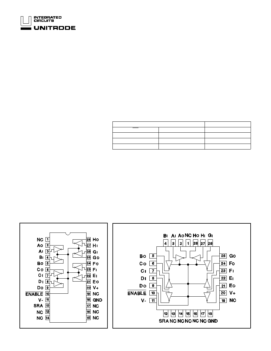
CONNECTION DIAGRAMS
N PACKAGE (TOP VIEW)
Q PACKAGE (TOP VIEW)
V+ (Pin 20) . . . . . . . . . . . . . . . . . . . . . . . . . . . . . . . . . . . . . . . . . . . . . . . . . . 15V
V- (Pin 11) . . . . . . . . . . . . . . . . . . . . . . . . . . . . . . . . . . . . . . . . . . . . . . . . . . -15V
PLCC Power Dissipation, T
A
=25
∞
C (Note 3) . . . . . . . . . . . . . . . . . . . 1000 mW
DIP Power Dissipation, T
A
=25
∞
C (Note 3) . . . . . . . . . . . . . . . . . . . . . 1250 mW
Input Voltage . . . . . . . . . . . . . . . . . . . . . . . . . . . . . . . . . . . . . . . . . . -1.5V to +7V
Output Voltage . . . . . . . . . . . . . . . . . . . . . . . . . . . . . . . . . . . . . . . . . -6V to +6V
Slew Rate Resistor . . . . . . . . . . . . . . . . . . . . . . . . . . . . . . . . . . . . . . 2k to 10k
Storage Temperature . . . . . . . . . . . . . . . . . . . . . . . . . . . . . . . -65
∞
C to +150
∞
C
Note 1: All voltages are with respect to ground, pin 18.
Note 3: Consult Packaging section of Databook for thermal limitations and
considerations of package.
UC5172
The UC5172 is a single-ended octal line driver designed to meet both
standard modem control applications (EIA232E/V.28), and long line
drive applications (EIA423A/V.10/X.26). The slew rate for all 8 drivers
is controlled by a single external resistor. The slew rate and output lev-
els are independent of the power variations.
The UC5172 has high output current, and current balance for long line
drive applications. EOS - Output parasitic SCRs powered on and off
are 35V, well above signal levels, allowing protection devices to work.
Inputs are compatible TTL+MOS logic families and are diode protected
against negative transients.
∑
Eight Single-Ended Line Drivers in One
Package
∑
Meets Standards EIA232E/CCITT V.28,
and EIA423A/CCITT V.10/X.26
∑
Single External Resistor Controls Slew
Rate
∑
Wide Supply Voltage Range
∑
Tri-State Outputs
∑
Output Short-Circuit Protection
∑
Low Power Consumption
∑
2kV ESD Protection on all Pins
∑
EOS on all Output Pins 35V under all
Output Conditions
∑
High Current Output for Long Line
Drive, Exceeds Standards
FEATURES
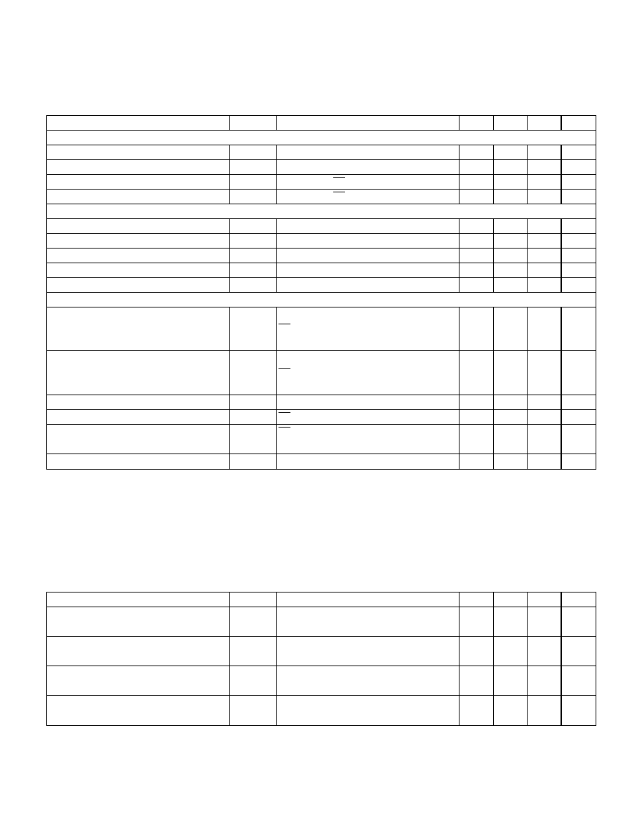
ABSOLUTE MAXIMUM RATINGS (Note 1)
FUNCTIONAL TABLE
9/96
DESCRIPTION
PARAMETER
SYMBOL
TEST CONDITIONS
MIN
TYP
MAX
UNITS
POWER SUPPLY REQUIREMENTS
V+ Range
9
15
V
V- Range
-9
-15
V
V+ Supply Current
I+
R
L
= Infinite En = 0V
15
25
mA
V- Supply Current
I-
R
L
= Infinite En = 0V
-17
-25
mA
INPUTS
High-Level Input Voltage
V
IH
2.0
V
Low-Level Input Voltage
V
IL
0.8
V
Input Clamp Voltage
V
IK
I
I
= -15 mA
-1.1
-18
V
High Level Input Current
I
IH
V
IH
= 2.4V
-2
0.25
40
µ
A
Low Level Input Current
I
IL
V
IL
= 0.4V
-200
-8.0
µ
A
OUTPUTS
High Level Output Voltage
V
OH
V
IN
= 0.8V
R
L
= Inf.
5.0
5.3
6.0
V
EIA232E
En = 0.8V
R
L
= 3k
5.0
5.3
6.0
V
(EIA-423A)
R
L
= 450
4.5
5.2
6.0
V
Low Level Output Voltage
V
OL
V
IN
= 2.0V
R
L
= Inf.
-5.0
-5.3
-6.0
V
EIA232E
En = 0.8V
R
L
= 3k
-5.0
-5.6
-6.0
V
(EIA-423A)
R
L
= 450
-4.5
-5.4
-6.0
V
Output Balance (EIA-423A)
V
BAL
R
L
= 450, V
OH
- V
OL
= V
BAL
0.2
0.4
V
Off-State Output Current
I
OZ
En = 2.0V, V
O
=
±
6V, V+ = 15V, V
-
= -15V
-100
100
µ
A
Short-Circuit Current
I
OS
En = 0V
V
IN
= 0V
25
65
mA
V
IN
= 5V
25
70
mA
Power Off Output Current
I
PO
V
O
=
±
6V, V+ = V
-
= 0V
-100
100
mA
UC5172
DC ELECTRICAL CHARACTERISTICS:
AC ELECTRICAL CHARACTERISTICS:
PARAMETER
SYMBOL
TEST CONDITIONS
MIN
TYP
MAX
UNITS
Output Slew Rate
t
R
R
SRA
= 2k
7.6
8.5
9.4
V/
µ
s
t
F
R
L
= 450, C
L
= 50pF
7.6
8.5
9.4
V/
µ
s
Output Slew Rate
t
R
R
SRA
= 10k
1.5
1.7
1.9
V
µ
s
t
F
R
L
= 450, C
L
= 50pF
1.5
1.7
1.9
V/
µ
s
Propagation Output
to High Impedance
t
Hz
R
SRA
= 10k
0.8
2.0
µ
s
t
Lz
R
L
= 450, C
L
= 50pF
0.5
2.0
µ
s
Propagation High
Impedance to Output
t
zH
R
SRA
= 10k
2.0
7.0
ms
t
zL
R
L
= 450, C
L
= 50pF
1.0
7.0
µ
s
Unless otherwise stated these specifications hold for |V+| = |V-| = 10V,
0
∞
C < T
A
< +70
∞
C, R
SRA
= +10k, T
A
=T
J.
at |V+| = |V-| = +10V, 0
∞
C < T
A
< +70
∞
C, T
A
= T
J.
2
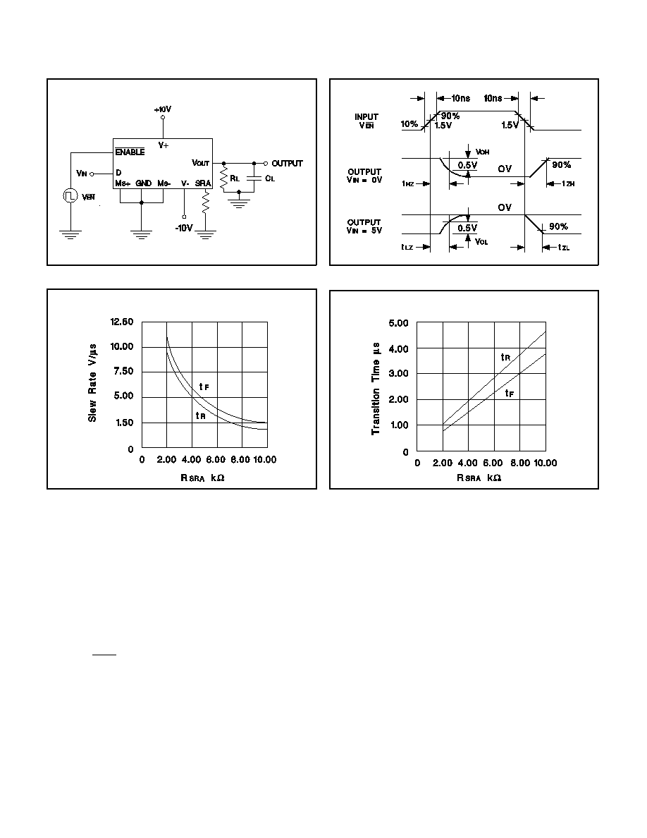
AC PARAMETER TEST CIRCUIT AND WAVEFORMS
UC5172
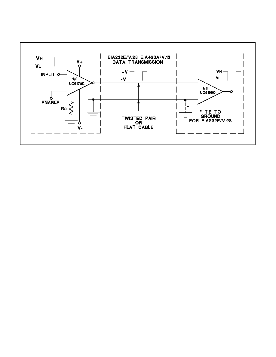
APPLICATIONS
Slew Rate Programming
Slew rate for the UC5172 is set up by a single external re-
sistor connected between the SRA pin and ground. Slew
rate adjustments can be approximated by using the fol-
lowing formula:
V/
µ
s
=
20
R
SRA
(R
SRA
in k
)
The slew rate resistor can vary between 2k and 10k
which allows slew rates between 10 to 2.2V/
µ
s, respec-
tively. The relationship between slew rate and R
SRA
is
shown in the typical characteristics.
Waveshaping of the output lets the user control the level
of interference (near-end crosstalk) that may be coupled
to adjacent circuits in an interconnection. The recom-
mended output characteristics for cable length and data
rates can be found in EIA standard EIA-423A. Approxima-
tions of these standards are given by the following equa-
tions:
Max. Data Rate = 300/t (For data rates 1k to 100k bit/s)
Max. Cable Length (feet) = 100 x t (Max. length 4000
feet)
where t is the transition time from 10% to 90% of the out-
put swing in microseconds. For data rates below 1k bit/s,
t may be up to 300 microseconds.
The UC5172 has been used in applications up to
460KBPS.
AC CHARACTERISTICS
Driver Slew Rate
Driver t
R
& t
F
(10-90%) EIA-423A Mode
3
Filter connectors or transzorbs should be used to reduce
the RFI/EMI, protecting the system from static (ESD), and
electrical overstress (EOS). A filter connector or capacitor
will reduce the ESD pulse by 90% typically. A cable
dragged across a carpet and connected to a system can
easily be charged to over 25,000 volts. This is a metal to
metal contact when the cable is connected to the system
(no resistance), currents exceed 80 amps with less than a
nanosecond rise time. A transzorb provides two functions,
the device capacitance inherently acts as a filter capaci-
tor, and the device clamps the ESD and EOS pulses
which would pass through the capacitor and destroy the
devices. The recommended transzorb for the UC5172 is
P6KEIOCA.
*Transzorb is a trademark of General Semiconductor
Industries.
UC5172
Specific Layout Notes
The UC5172 layout must have bulk bypassing close to
the device. Peak slew current is greater than 500mA
when all eight drivers slew at once in the same direction.
Some applications mount the UC5172 on a bulkhead or
isolated plane for RFI/FCC/VDE reasons. If bulk bypass-
ing is not used, the -10V supply may go above -8.5 volts,
causing the slew rate control circuit to become unstable.
The UC5172 can have output oscillation at 100kHz if the
+10V supply is applied before the -10V supply. This has
been a problem in some terminal designs where the +10V
was developed from the flyback, which can result in a
500ms difference in the application of the supplies at
power up.
General Layout Notes
The drivers and receivers should be mounted close to the
system common ground point, with the ground reference
tied to the common point to reduce RFI/EMI.
UNITRODE INTEGRATED CIRCUITS
7 CONTINENTAL BLVD.
∑
MERRIMACK, NH 03054
TEL. (603) 424-2410
∑
FAX 603) 424-3460
APPLICATIONS
4

IMPORTANT NOTICE
Texas Instruments and its subsidiaries (TI) reserve the right to make changes to their products or to discontinue
any product or service without notice, and advise customers to obtain the latest version of relevant information
to verify, before placing orders, that information being relied on is current and complete. All products are sold
subject to the terms and conditions of sale supplied at the time of order acknowledgement, including those
pertaining to warranty, patent infringement, and limitation of liability.
TI warrants performance of its semiconductor products to the specifications applicable at the time of sale in
accordance with TI's standard warranty. Testing and other quality control techniques are utilized to the extent
TI deems necessary to support this warranty. Specific testing of all parameters of each device is not necessarily
performed, except those mandated by government requirements.
CERTAIN APPLICATIONS USING SEMICONDUCTOR PRODUCTS MAY INVOLVE POTENTIAL RISKS OF
DEATH, PERSONAL INJURY, OR SEVERE PROPERTY OR ENVIRONMENTAL DAMAGE ("CRITICAL
APPLICATIONS"). TI SEMICONDUCTOR PRODUCTS ARE NOT DESIGNED, AUTHORIZED, OR
WARRANTED TO BE SUITABLE FOR USE IN LIFE-SUPPORT DEVICES OR SYSTEMS OR OTHER
CRITICAL APPLICATIONS. INCLUSION OF TI PRODUCTS IN SUCH APPLICATIONS IS UNDERSTOOD TO
BE FULLY AT THE CUSTOMER'S RISK.
In order to minimize risks associated with the customer's applications, adequate design and operating
safeguards must be provided by the customer to minimize inherent or procedural hazards.
TI assumes no liability for applications assistance or customer product design. TI does not warrant or represent
that any license, either express or implied, is granted under any patent right, copyright, mask work right, or other
intellectual property right of TI covering or relating to any combination, machine, or process in which such
semiconductor products or services might be or are used. TI's publication of information regarding any third
party's products or services does not constitute TI's approval, warranty or endorsement thereof.
Copyright
©
1999, Texas Instruments Incorporated