 | –≠–ª–µ–∫—Ç—Ä–æ–Ω–Ω—ã–π –∫–æ–º–ø–æ–Ω–µ–Ω—Ç: UC5350N | –°–∫–∞—á–∞—Ç—å:  PDF PDF  ZIP ZIP |
UC5350
CAN TRANSCEIVER
SLUS258C ≠ MARCH 2000 ≠ REVISED DECEMBER 2001
1
POST OFFICE BOX 655303
∑
DALLAS, TEXAS 75265
D
Pin Compatible With PCA82C250 and
DeviceNet, SDS
D
ISO11898 Compatible
D
High Speed, up to 1 Mbps
D
Differential Transmit to the Bus and
Receive From the Bus to the CAN
Controller
D
At Least 110 Nodes Can Be Connected
D
100-V Transient Protection on the Transmit
Output
D
24-V Supply Cross Wire Protection on
CANH and CANL
D
No Bus Loading When Powered Down
D
Operates Between ≠40
∞
C to 85
∞
C
D
Unitrode DeviceNet ID#107
description
The UC5350 control area network (CAN) transceiver is designed for industrial applications employing the CAN
serial communications physical layer per ISO 11898 standard. The device is a high-speed transceiver designed
for use up to 1 Mbps. Especially designed for hostile environments, this device features cross wire, loss of
ground, overvoltage, and overtemperature protections as well as a wide common-mode range.
The transceiver interfaces the single-ended CAN controller with the differential CAN bus found in industrial and
automotive applications. It operates over the ≠7-V to 12-V common-mode range of the bus and will withstand
common-mode transients of ≠25 V to 18 V as well as Schaffner tests. Performance features include high
differential-input impedance, a symmetrical-differential-signal driver, and very-low propogation delay that
improves bus bandwidth and length by reducing reflection and distortion.
The transceiver operates over a wide temperature range, ≠40
∞
C to 85
∞
C and is available in 8-pin SOIC and
dual-in-line packages.
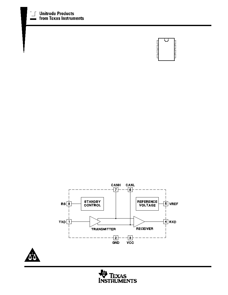
block diagram
UDG-96202
Copyright
2001, Texas Instruments Incorporated
PRODUCTION DATA information is current as of publication date.
Products conform to specifications per the terms of Texas Instruments
standard warranty. Production processing does not necessarily include
testing of all parameters.
Please be aware that an important notice concerning availability, standard warranty, and use in critical applications of
Texas Instruments semiconductor products and disclaimers thereto appears at the end of this data sheet.
1
2
3
4
8
7
6
5
TXN
GND
VCC
RXD
RS
CANH
CANL
VREF
D AND N PACKAGE
(TOP VIEW)
NOTE:
THIS PRODUCT IS NOT RECOMMENDED
FOR NEW DESIGNS. IT WILL SOON BE
REPLACED BY PART NUMBER
SN65HVD251.
UC5350
CAN TRANSCEIVER
SLUS258C ≠ MARCH 2000 ≠ REVISED DECEMBER 2001
2
POST OFFICE BOX 655303
∑
DALLAS, TEXAS 75265
functional table (VCC = 4.5 V to 5.5 V)
Inputs
System Mode
O tp t Mode
Outputs
TXD
RS
System Mode
Output Mode
VCANH ≠ VCANL
RXD
0
0
High speed
Dominant
1.5 V to 3 V
0
1
0
High speed
Recessive
≠120 mV to 12 mV
1
High Z
0
High speed
Recessive
≠120 mV to 12 mV
1
X
1
Standb
High Z
0 at Bus = Dominant
X
1
Standby
--
High Z
1 at Bus = Recessive
absolute maximum ratings over operating free-air temperature (unless otherwise noted)
}
Supply voltage
≠0.3 V to 9 V
. . . . . . . . . . . . . . . . . . . . . . . . . . . . . . . . . . . . . . . . . . . . . . . . . . . . . . . . . . . . . . . . . . . . .
TXD, RXD, VREF, RS
≠0.3 V to VCC + 0.3 V
. . . . . . . . . . . . . . . . . . . . . . . . . . . . . . . . . . . . . . . . . . . . . . . . . . . . . .
CANL, CANH, (0 V < VCC < 5.5 V)
≠8 V to 36 V
. . . . . . . . . . . . . . . . . . . . . . . . . . . . . . . . . . . . . . . . . . . . . . . . . . . .
CANL, CANH, (non-destructive, non-operative)
≠8 V to 32 V
. . . . . . . . . . . . . . . . . . . . . . . . . . . . . . . . . . . . . . . . .
CANL, CANH, (transient, Schaffner test) See Figure 1
≠150 V to 100 V
. . . . . . . . . . . . . . . . . . . . . . . . . . . . . . . .
Operating temperature
≠40
∞
C to 85
∞
C
. . . . . . . . . . . . . . . . . . . . . . . . . . . . . . . . . . . . . . . . . . . . . . . . . . . . . . . . . . . .
Storage temperature, T
stg
≠65
∞
C to 150
∞
C
. . . . . . . . . . . . . . . . . . . . . . . . . . . . . . . . . . . . . . . . . . . . . . . . . . . . . . . . .
Junction temperature, T
J
≠55
∞
C to 150
∞
C
. . . . . . . . . . . . . . . . . . . . . . . . . . . . . . . . . . . . . . . . . . . . . . . . . . . . . . . . . .
Lead temperature (soldering, 10 sec.)
300
∞
C
. . . . . . . . . . . . . . . . . . . . . . . . . . . . . . . . . . . . . . . . . . . . . . . . . . . . . .
Crosswire protection maximum VBUS
30 V
. . . . . . . . . . . . . . . . . . . . . . . . . . . . . . . . . . . . . . . . . . . . . . . . . . . . . . . .
Bus differential voltage
k
30 V
. . . . . . . . . . . . . . . . . . . . . . . . . . . . . . . . . . . . . . . . . . . . . . . . . . . . . . . . . . . . . . . . . . . .
Cross wire protection T
A
≠40
∞
C to 125
∞
C
. . . . . . . . . . . . . . . . . . . . . . . . . . . . . . . . . . . . . . . . . . . . . . . . . . . . . . . . . .
Stresses beyond those listed under "absolute maximum ratings" may cause permanent damage to the device. These are stress ratings only, and
functional operation of the device at these or any other conditions beyond those indicated under "recommended operating conditions" is not
implied. Exposure to absolute-maximum-rated conditions for extended periods may affect device reliability.
Currents are positive into, negative out of the specified terminal. Consult Packaging Section of the Interface Products Data Book (TI Literature
Number SLUU002) for thermal limitations and considerations of packages.
k
Refers to Figures 9, 10, 11, 12 and 13.
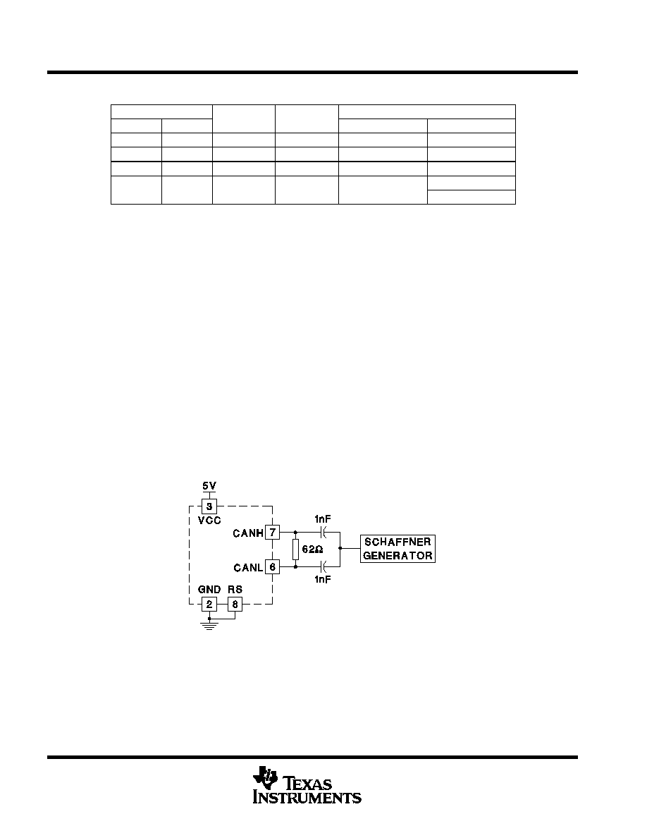
NOTE: See Figure 7 for pulse timing.
UDG-96203-1
Figure 1. Schaffner Test
UC5350
CAN TRANSCEIVER
SLUS258C ≠ MARCH 2000 ≠ REVISED DECEMBER 2001
3
POST OFFICE BOX 655303
∑
DALLAS, TEXAS 75265
electrical characteristics (
total device disconnected from the bus line), VCC = 4.5 V to 5.5 V, 60
in parallel
with 100-pF load between CANH and CANL, T
A
= ≠40
∞
C to 85
∞
C, T
A
= T
J
, (unless otherwise stated)
PARAMETER
TEST CONDITIONS
MIN
TYP
MAX
UNITS
Supply voltage
4.5
5.5
V
Dominant,
TXD = 1 V
70
mA
Supply current
Recessive,
TXD = 4 V
9
14
mA
Su
ly current
Standby,
RS = 4 V
1.2
2.0
mA
RS input current
≠10
5
µ
A
RS voltage input = logic 1
Standby
0.75VCC
V
RS voltage input = logic 0
High speed
0.3VCC
V
Transmitter voltage input = logic 1
Transmitter output recessive
0.7VCC
V
Transmitter voltage input = logic 0
Transmitter output dominant
0.3VCC
V
Transmitter current input at logic 1
TXD = 4 V
30
µ
A
Transmitter current input at logic 0
TXD = 1 V
≠30
30
µ
A
Receiver voltage output = logic 1
RXD = ≠100 mA,
TXD = 4 V
VCC
≠1.25
V
Recei er oltage o tp t
logic 0
RXD = 1 mA,
TXD = 1 V
0.75
1.2
V
Receiver voltage output = logic 0
RXD = 10 mA,
TXD = 1 V
1.2
1.7
V
CANH, CANL input resistance
No load,
TXD = 4 V
20
40
k
Differential input resistance
No load,
TXD = 4 V
40
80
k
CANH, CANL input capacitance
See Note 1
20
pF
Differential input capacitance
See Note 1
10
pF
Reference output voltage
VREF =
±
50 mA
0.45VCC
0.55VCC
V
NOTE 1: Ensured by design. Not production tested.
UC5350
CAN TRANSCEIVER
SLUS258C ≠ MARCH 2000 ≠ REVISED DECEMBER 2001
4
POST OFFICE BOX 655303
∑
DALLAS, TEXAS 75265
electrical characteristics,
(dc parameters for recessive state disconnected from the bus line), 60
in
parallel with 100-pF load between CANH and CANL, T
A
= ≠40
∞
C to 85
∞
C, T
A
= T
J
, (unless otherwise stated)
PARAMETER
TEST CONDITIONS
MIN
TYP
MAX
UNITS
VCANH, VCANL
No load,
TXD = 4 V,
See Figure 2
2
2.5
3
V
Differential output transmitter
(VCANH ≠ VCANL)
No load,
TXD = 4 V,
See Figure 2
≠500
0
50
mV
Differential input receiver
Common mode range = ≠7 V to 12 V,
TXD = 4 V,
CANH, CANL externally driven
See Figure 3
≠1
0.40
V
Differential input resistance
No load
40
k
CANH, CANL input resistance
20
k
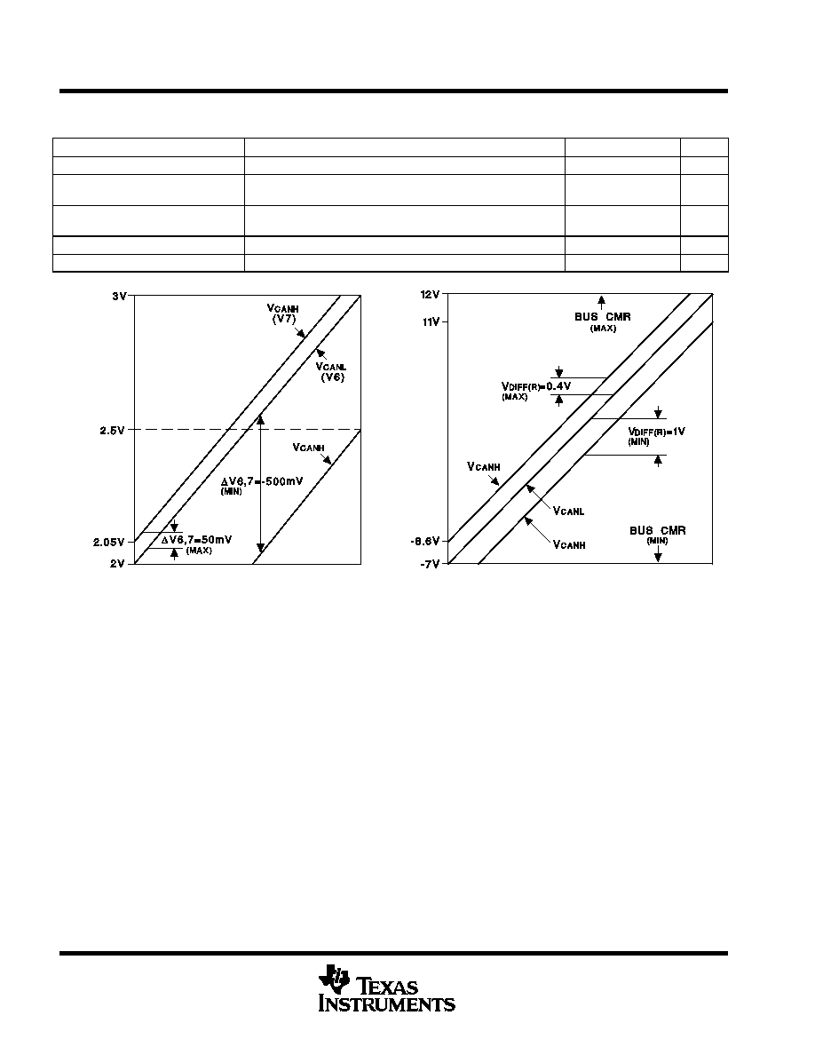
Figure 2. Recessive State Voltage Diagram
NOTE: Valid output of CANH, CANL during recessive state
transmission. TXD = LOGIC 1
UDG-96204
Figure 3. Recessive State Voltage Diagram
NOTE: Valid voltage range of VCANH for sensing dominant bus
state as VCANL varies over bus common range mode. TXD
= LOGIC1
UDG-96205
UC5350
CAN TRANSCEIVER
SLUS258C ≠ MARCH 2000 ≠ REVISED DECEMBER 2001
5
POST OFFICE BOX 655303
∑
DALLAS, TEXAS 75265
electrical characteristics, (dc parameters for dominant state disconnected from the bus line), 60
in parallel with 100-pF load between CANH and CANL. VCC = 4.5 V to 5.5 V, ) (unless otherwise
stated)
PARAMETER
TEST CONDITIONS
MIN
TYP
MAX
UNITS
CANH output voltage (VCANH)
TXD = 1 V,
See Figure 4
2.75
4.5
V
CANL output voltage (VCANL)
TXD = 1 V,
See Figure 4
0.50
1.1
2.25
V
Differential output transmitter
(VCANH ≠ VCANL)
TXD = 1 V,
See Figure 4
1.5
2
3
V
Differential input receiver (VDIFF(D))
Common mode range = ≠2 to 7 V,
TXD = 4 V,
CANH, CANL externally driven,
See Figure 5
0.9
5
V
Common mode range = ≠7 to 12 V,
TXD = 4 V,
CANH, CANL externally driven,
See Figure 5
1.0
5
V
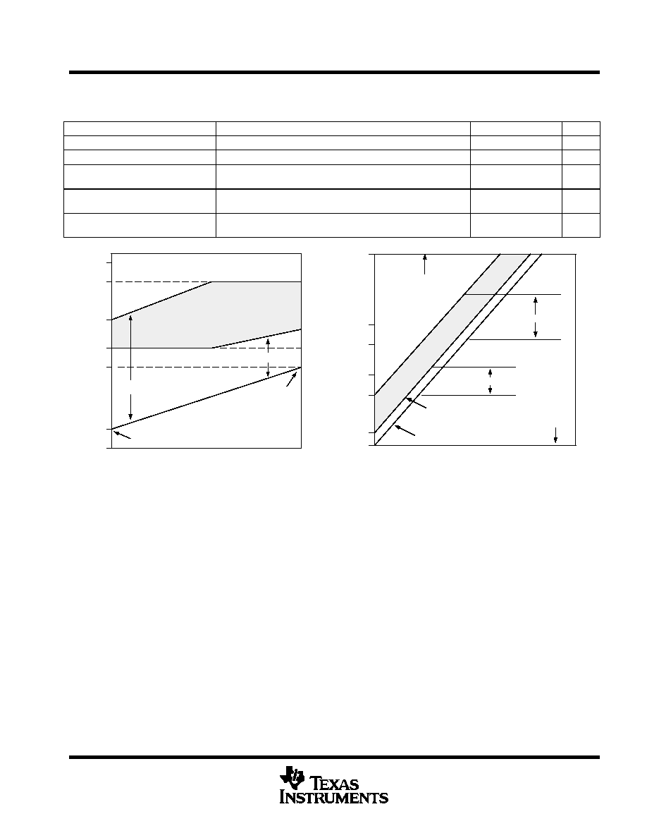
Figure 4. Dominant State Voltage Diagram
NOTE: Valid voltage range of VCANH for sensing dominant bus state
as VCANL varies. TXD = LOGIC 0
0.5 V
2.25V
2.75 V
3.5 V
4.5 V
5V
RANGE OF V CANH (SHADED)
VCANH (MAX)
VCANH (MIN)
VCANL (MIN)
VCANL (MAX)
V6,7 = 3 V (MAX)
UDG-97160
V6,7 = 1.5 V (MIN)
Figure 5. Dominant State Voltage Diagram
≠7 V
≠2 V
0 V
≠6.1 V
12 V
BUS CMR (MAX)
VCANL
5 V
BUS CMR (MIN)
VCANH
VDIFF(D) = 0.9 V (MIN)
VDIFF(D) = 5 V (MAX)
NOTE: Valid voltage range of VCANH for sensing dominant bus
state as VCANL varies over bus common mode range. TXD
= LOGIC 0
UDG-97160