
∑
Complies with SCSI, SCSI-2
Standards
∑
10pF Channel Capacitance During
Disconnect
∑
Active Termination for 18 Lines
∑
Logic Command Disconnects all
Termination Lines
∑
Low Supply Current in Disconnect
Mode
∑
Trimmed Regulator for Accurate
Termination Current
∑
Current Limit and Thermal
Shutdown Protection
∑
110 Ohm Termination
∑
Meets SCSI Hot Plugging
The UC5601 provides precision resistive pull-up to a 2.9V reference for all
18 lines in a Small Computer Systems Interface (SCSI) bus cable. The
SCSI-2 standard recommends active termination at both ends of every ca-
ble segment utilizing single ended drivers and receivers.
Internal circuit trimming is utilized, first to reduce resistor tolerances to
±
3%
and then to adjust the regulator's output voltage to insure termination cur-
rent accuracy of
±
3%.
The UC5601 provides a disconnect feature which, upon a logic command,
disconnects all terminating resistors, and turns off the regulator; greatly re-
ducing standby power.
Other features include negative clamping on all signal lines, 20mA of active
negation sink current capability, regulator current limiting, and thermal shut-
down protection.
This device is offered in low thermal resistance versions of the industry
standard 28 pin wide body SOIC and PLCC, as well as a 24 pin DIL plastic
package.
UC5601
SCSI Active Terminator
FEATURES DESCRIPTION
BLOCK DIAGRAM
Circuit Design Patented
10/94
UDG-94060
ABSOLUTE MAXIMUM RATINGS
Termpwr Voltage . . . . . . . . . . . . . . . . . . . . . . . . . . . . . . . . . +7V
Signal Line Voltage. . . . . . . . . . . . . . . . . . . . . . . . . . . 0V to +7V
Regulator Output Current . . . . . . . . . . . . . . . . . . . . . . . . . . . . 1A
Storage Temperature . . . . . . . . . . . . . . . . . . .
-
-
65∞C to +150∞C
Operating Temperature . . . . . . . . . . . . . . . . .
-
-
55∞C to +150∞C
Lead Temperature (Soldering, 10 Sec.) . . . . . . . . . . . . . +300∞C
RECOMMENDED OPERATING CONDITIONS
Termpwr Voltage . . . . . . . . . . . . . . . . . . . . . . . . . 4.0V to 5.25V
Signal Line Voltage. . . . . . . . . . . . . . . . . . . . . . . . . . . 0V to +3V
Disconnect Input Voltage . . . . . . . . . . . . . . . . . . 0V to Termpwr
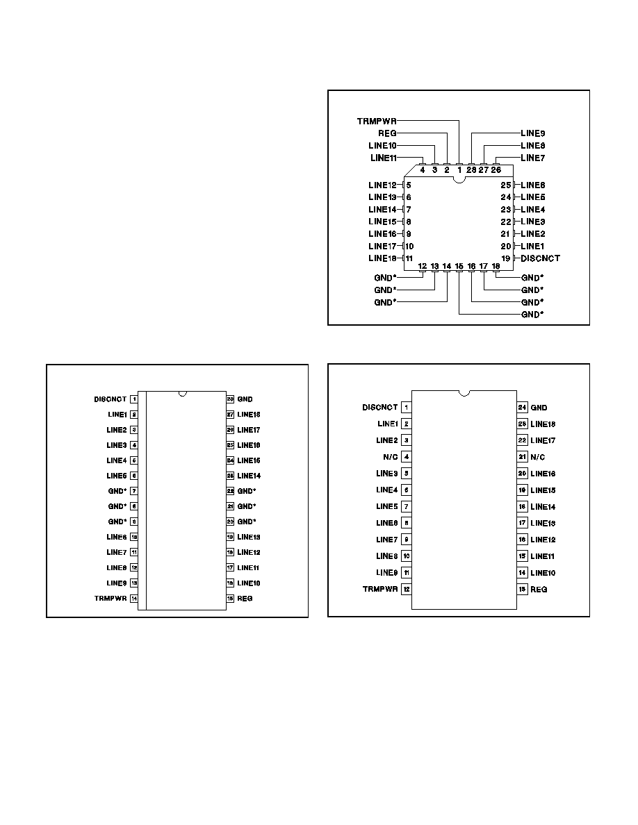
CONNECTION DIAGRAMS
UC5601
Note: Drawings are not to scale.
Unless otherwise specified all voltages are with respect to
Ground. Currents are positive into, negative out of the speci-
fied terminal.
Consult Packaging Section of Unitrode Integrated Circuits dat-
abook for thermal limitations and considerations of packages.
* QP package pins 12 - 18 serve as both heatsink and signal
ground.
* DWP package pin 28 serves as signal ground; pins 7, 8, 9,
20, 21, 22 serve as heatsink/ground.
SOIC-28 (Top View)
DWP Package
DIL-24 (Top View)
N or J Package
PLCC-28 (Top View)
QP Package
2
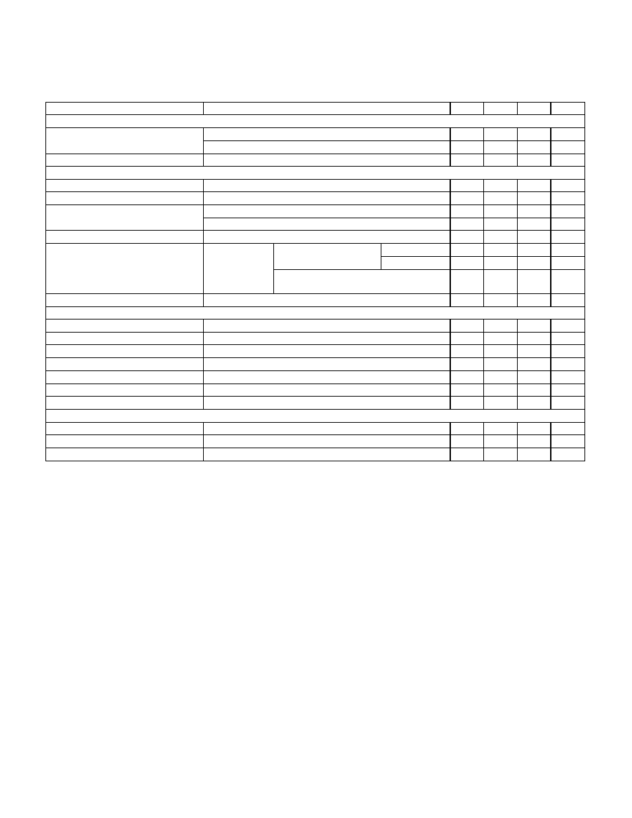
PARAMETER
TEST CONDITIONS
MIN
TYP
MAX
UNITS
Supply Current Section
Termpwr Supply Current
All termination lines = Open
17
25
mA
All termination lines = 0.5V
400
430
mA
Power Down Mode
DISCNCT = Open
100
150
µ
A
Output Section (Termination Lines)
Termination Impedance
I
LINE
= -5mA to -15mA
107
110
113
Output High Voltage
V
TRMPWR
= 4V (Note 1)
2.65
2.9
V
Max Output Current
V
LINE
= 0.5V
-21.1
-21.7
-22.4
mA
V
LINE
= 0.5V, TRMPWR = 4V (Note 1)
-19.8
-21.7
-22.4
mA
Output Clamp Level
I
LINE
= -30mA
-0.2
-0.05
0.1
V
Output Leakage
DISCNCT = 4V
TRMPWR = 0V to 5.25V
REG = 0V
V
LINE
= 0 to 4V
10
400
nA
V
LINE
= 5.25V
100
µ
A
TRMPWR = 0V to 5.25V, REG = Open
V
LINE
= 0V to 5.25V
10
400
nA
Output Capacitance
DISCNCT = Open (Note 2)
10
12
pF
Regulator Section
Regulator Output Voltage
2.8
2.9
3.0
V
Line Regulation
TRMPWR = 4V to 6V
10
20
mV
Load Regulation
I
REG
= 0 to -400mA
20
50
mV
Drop Out Voltage
All Termination Lines = 0.5V
1.0
1.2
V
Short Circuit Current
V
REG
= 0V
-450
-650
-850
mA
Current Sink Capability
V
REG
= 3.5V
8
20
25
mA
Thermal Shutdown
170
∞C
Disconnect Section
Disconnect Threshold
1.3
1.5
1.7
V
Threshold Hysteresis
100
160
250
mV
Input Current
DISCNCT = 0V
10
15
µ
A
ELECTRICAL CHARACTERISTICS
Unless otherwise stated, these specifications apply for T
A
= 0∞C to 70∞C.
TRMPWR = 4.75V, DISCNCT = 0V. T
A
= T
J
.
UC5601
Note 1: Measuring each termination line while other 17 are low (0.5V).
Note 2: Guaranteed by design. Not 100% tested in production.
QP package: (see packaging section of UICC data book for more details on thermal performance)
Thermal Resistance Junction to Leads,
jL . . . . . . . . . . . . . . . . . . . . . . . . . . . . . . . . . . . . . . . . . . . . . . 15∞C/W
Thermal Resistance Junction to Ambient,
ja . . . . . . . . . . . . . . . . . . . . . . . . . . . . . . . . . . . . . . . . . . 30∞-40∞C/W
DWP package:
Thermal Resistance Junction to Leads,
jL . . . . . . . . . . . . . . . . . . . . . . . . . . . . . . . . . . . . . . . . . . . . . . 18∞C/W
Thermal Resistance Junction to Ambient,
ja . . . . . . . . . . . . . . . . . . . . . . . . . . . . . . . . . . . . . . . . . . 33∞-43∞C/W
J package:
Thermal Resistance Junction to Leads,
jL . . . . . . . . . . . . . . . . . . . . . . . . . . . . . . . . . . . . . . . . . . . . . . 40∞C/W
Thermal Resistance Junction to Ambient,
ja . . . . . . . . . . . . . . . . . . . . . . . . . . . . . . . . . . . . . . . . . . 75∞-85∞C/W
N package:
Thermal Resistance Junction to Leads,
jL . . . . . . . . . . . . . . . . . . . . . . . . . . . . . . . . . . . . . . . . . . . . . . 50∞C/W
Thermal Resistance Junction to Ambient,
ja . . . . . . . . . . . . . . . . . . . . . . . . . . . . . . . . . . . . . . . . . 95∞-105∞C/W
THERMAL DATA
Note: The above numbers for
jL are maximums for the limiting thermal resistance of the package in a standard mounting configu-
ration. The
ja numbers are meant to be guidelines for the thermal performance of the device/pc-board system. All of the above
numbers assume no ambient airflow.
3
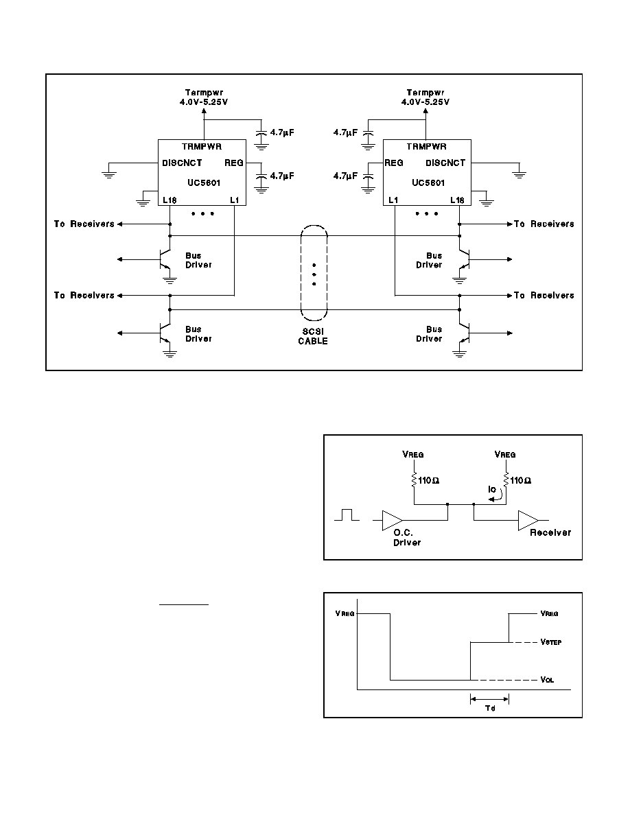
Typical SCSI Bus Configuration Using the UC5601
UC5601
A Look at the Response of a SCSI-2 Cable
Figure 1 shows a single line of a SCSI cable. The driver
is an open colletor type which when asserted pulls low,
and when negated the termination resistance serves as
the pull-up.
Figure 2 shows a worst case scenario of mid cable de-
assertion with a close proximity receiver. The voltage
V
STEP
is defined as:
V
STEP
= V
OL
+I
O
Z
0
V
OL
=
Driver Output Low Voltage
I
O
=
Current from Receiving Terminator
Z
0
=
Cable Characteristic Impedance
I
O
=
V
REG
-
V
OL
110
In the pursuit of higher data rates, sampling culd occur
during this step portion, therefore it is important to ensure
that the step is as high as possible to get the most noise
margin. For this reason the UC5601 is trimmed so that
the output current (I
O
) is as close as possible to the SCSI
max current spec of 22.4mA. The Termination impedance
is initially trimmed on the IC to 110 ohms typical, then the
regulator voltage is trimmed for the highest output cur-
rent to within 22.4mA.
Figure 1. A Single Line of a SCSI Cable
Figure 2. A Typical Response of a SCSI Cable
UDG-94062
UDG-94063
UDG-94061
UNITRODE INTEGRATED CIRCUITS
7 CONTINENTAL BLVD.
∑
∑
MERRIMACK, NH 03054
TEL. (603) 424-241
0 ∑
FAX (603) 424 3460
4
PACKAGING INFORMATION
Orderable Device
Status
(1)
Package
Type
Package
Drawing
Pins Package
Qty
Eco Plan
(2)
Lead/Ball Finish
MSL Peak Temp
(3)
UC5601DWP
ACTIVE
SOIC
DW
28
20
None
CU SNPB
Level-2-220C-1 YEAR
UC5601DWPTR
ACTIVE
SOIC
DW
28
1000
None
CU SNPB
Level-2-220C-1 YEAR
UC5601DWPTRG4
ACTIVE
SOIC
DW
28
1000 Green (RoHS &
no Sb/Br)
CU NIPDAU
Level-2-260C-1 YEAR
UC5601N
ACTIVE
PDIP
N
24
15
None
CU SNPB
Level-NA-NA-NA
UC5601QP
ACTIVE
PLCC
FN
28
37
None
CU SNPB
Level-2-220C-1 YEAR
UC5601QPTR
ACTIVE
PLCC
FN
28
750
None
CU SNPB
Level-2-220C-1 YEAR
(1)
The marketing status values are defined as follows:
ACTIVE: Product device recommended for new designs.
LIFEBUY: TI has announced that the device will be discontinued, and a lifetime-buy period is in effect.
NRND: Not recommended for new designs. Device is in production to support existing customers, but TI does not recommend using this part in
a new design.
PREVIEW: Device has been announced but is not in production. Samples may or may not be available.
OBSOLETE: TI has discontinued the production of the device.
(2)
Eco Plan - May not be currently available - please check
http://www.ti.com/productcontent
for the latest availability information and additional
product content details.
None: Not yet available Lead (Pb-Free).
Pb-Free (RoHS): TI's terms "Lead-Free" or "Pb-Free" mean semiconductor products that are compatible with the current RoHS requirements
for all 6 substances, including the requirement that lead not exceed 0.1% by weight in homogeneous materials. Where designed to be soldered
at high temperatures, TI Pb-Free products are suitable for use in specified lead-free processes.
Green (RoHS & no Sb/Br): TI defines "Green" to mean "Pb-Free" and in addition, uses package materials that do not contain halogens,
including bromine (Br) or antimony (Sb) above 0.1% of total product weight.
(3)
MSL, Peak Temp. -- The Moisture Sensitivity Level rating according to the JEDECindustry standard classifications, and peak solder
temperature.
Important Information and Disclaimer:The information provided on this page represents TI's knowledge and belief as of the date that it is
provided. TI bases its knowledge and belief on information provided by third parties, and makes no representation or warranty as to the
accuracy of such information. Efforts are underway to better integrate information from third parties. TI has taken and continues to take
reasonable steps to provide representative and accurate information but may not have conducted destructive testing or chemical analysis on
incoming materials and chemicals. TI and TI suppliers consider certain information to be proprietary, and thus CAS numbers and other limited
information may not be available for release.
In no event shall TI's liability arising out of such information exceed the total purchase price of the TI part(s) at issue in this document sold by TI
to Customer on an annual basis.
PACKAGE OPTION ADDENDUM
www.ti.com
18-Feb-2005
Addendum-Page 1

IMPORTANT NOTICE
Texas Instruments Incorporated and its subsidiaries (TI) reserve the right to make corrections, modifications,
enhancements, improvements, and other changes to its products and services at any time and to discontinue
any product or service without notice. Customers should obtain the latest relevant information before placing
orders and should verify that such information is current and complete. All products are sold subject to TI's terms
and conditions of sale supplied at the time of order acknowledgment.
TI warrants performance of its hardware products to the specifications applicable at the time of sale in
accordance with TI's standard warranty. Testing and other quality control techniques are used to the extent TI
deems necessary to support this warranty. Except where mandated by government requirements, testing of all
parameters of each product is not necessarily performed.
TI assumes no liability for applications assistance or customer product design. Customers are responsible for
their products and applications using TI components. To minimize the risks associated with customer products
and applications, customers should provide adequate design and operating safeguards.
TI does not warrant or represent that any license, either express or implied, is granted under any TI patent right,
copyright, mask work right, or other TI intellectual property right relating to any combination, machine, or process
in which TI products or services are used. Information published by TI regarding third-party products or services
does not constitute a license from TI to use such products or services or a warranty or endorsement thereof.
Use of such information may require a license from a third party under the patents or other intellectual property
of the third party, or a license from TI under the patents or other intellectual property of TI.
Reproduction of information in TI data books or data sheets is permissible only if reproduction is without
alteration and is accompanied by all associated warranties, conditions, limitations, and notices. Reproduction
of this information with alteration is an unfair and deceptive business practice. TI is not responsible or liable for
such altered documentation.
Resale of TI products or services with statements different from or beyond the parameters stated by TI for that
product or service voids all express and any implied warranties for the associated TI product or service and
is an unfair and deceptive business practice. TI is not responsible or liable for any such statements.
Following are URLs where you can obtain information on other Texas Instruments products and application
solutions:
Products
Applications
Amplifiers
amplifier.ti.com
Audio
www.ti.com/audio
Data Converters
dataconverter.ti.com
Automotive
www.ti.com/automotive
DSP
dsp.ti.com
Broadband
www.ti.com/broadband
Interface
interface.ti.com
Digital Control
www.ti.com/digitalcontrol
Logic
logic.ti.com
Military
www.ti.com/military
Power Mgmt
power.ti.com
Optical Networking
www.ti.com/opticalnetwork
Microcontrollers
microcontroller.ti.com
Security
www.ti.com/security
Telephony
www.ti.com/telephony
Video & Imaging
www.ti.com/video
Wireless
www.ti.com/wireless
Mailing Address:
Texas Instruments
Post Office Box 655303 Dallas, Texas 75265
Copyright
2005, Texas Instruments Incorporated