
∑
Complies with SCSI, SCSI-2
Standards
∑
10pF Channel Capacitance During
Disconnect
∑
Active Termination for 18 Lines
∑
Logic Command Disconnects all
Termination Lines
∑
Low Supply Current in Disconnect
Mode
∑
Trimmed Regulator for Accurate
Termination Current
∑
Current Limit and Thermal
Shutdown Protection
∑
110 Ohm Termination
∑
Meets SCSI Hot Plugging
The UC5602 is a pin compatible version of its predecessor, the UC5601,
and is targeted for high volume applications which require active termina-
tion, but not the high performance of the UC5601. The major differences
are relaxed output current and termination tolerances, and the absence of
low side clamps.
The UC5602 provides 18 lines of active termination for a SCSI (Small
Computer Systems Interface) parallel bus. The SCSI-2 standard recom-
mends active termination at both ends of the cable segment, and SCSI-3
will make it a requirement.
The UC5602 provides a disconnect feature which, when opened or driven
high, will disconnect all terminating resistors, and disables the regulator;
greatly reducing standby power. The output channels remain high imped-
ance even without Termpwr applied.
Internal circuit trimming is utilized, first to trim the impedance to a 7% toler-
ance; and then most importantly, to trim the output current 7% tolerance,
as close to the max SCSI as possible, which maximizes noise margin in
fast SCSI operation.
Other features include thermal shutdown, current limit, and 40mA of active
negation sink current capability.
This device is offered in low thermal resistance versions of the industry
standard 28 pin wide body SOIC and PLCC, as well as a 24 pin DIL plastic
package.
UC5602
SCSI Active Terminator
FEATURES DESCRIPTION
BLOCK DIAGRAM
Circuit Design Patented
10/94
UDG-94052
ABSOLUTE MAXIMUM RATINGS
Termpwr Voltage . . . . . . . . . . . . . . . . . . . . . . . . . . . . . . . . . +7V
Signal Line Voltage. . . . . . . . . . . . . . . . . . . . . . . . . . . 0V to +7V
Regulator Output Current . . . . . . . . . . . . . . . . . . . . . . . . . . 0.5A
Storage Temperature . . . . . . . . . . . . . . . . . . .
-
-
65∞C to +150∞C
Operating Temperature . . . . . . . . . . . . . . . . .
-
-
55∞C to +150∞C
Lead Temperature (Soldering, 10 Sec.) . . . . . . . . . . . . . +300∞C
RECOMMENDED OPERATING CONDITIONS
Termpwr Voltage . . . . . . . . . . . . . . . . . . . . . . . . . 4.0V to 5.25V
Signal Line Voltage. . . . . . . . . . . . . . . . . . . . . . . . . . . 0V to +3V
Disconnect Input Voltage . . . . . . . . . . . . . . . . . . 0V to Termpwr
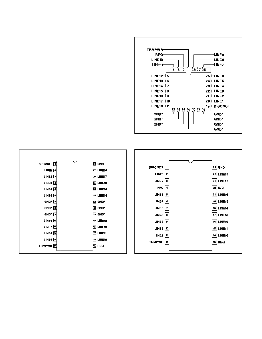
CONNECTION DIAGRAMS
UC5602
Note: Drawings are not to scale.
Unless otherwise specified all voltages are with respect to
Ground. Currents are positive into, negative out of the speci-
fied terminal.
Consult Packaging Section of Unitrode Integrated Circuits dat-
abook for thermal limitations and considerations of packages.
* QP package pins 12 - 18 serve as both heatsink and signal
ground.
* DWP package pin 28 serves as signal ground; pins 7, 8, 9,
20, 21, 22 serve as heatsink/ground.
SOIC-28 (Top View)
DWP Package
DIL-24 (Top View)
N Package
PLCC-28 (Top View)
QP Package
2

PARAMETER
TEST CONDITIONS
MIN
TYP
MAX
UNITS
Supply Current Section
Termpwr Supply Current
All termination lines = Open
20
29
mA
All termination lines = 0.5V
400
435
mA
Power Down Mode
DISCNCT = Open
100
150
µ
A
Output Section (Termination Lines)
Termination Impedance
I
LINE
= -5mA to -15mA
TJ = 25
∞
C
102
110
118
0∞C < T
J
< 70∞C
97
129
Output High Voltage
V
TRMPWR
= 4V (Note 1)
T
J
= 25
∞
C
2.6
2.9
3.1
V
0∞C < T
J
< 70∞C
2.55
3.2
V
Max Output Current
V
LINE
= 0.5V
T
J
= 25
∞
C
-19.5
-21.4
-22.4
mA
0∞C < T
J
< 70∞C
-18.5
-22.4
mA
Max Output Current
V
LINE
= 0.5V, TRMPWR = 4V (Note 1)
T
J
= 25
∞
C
-18.0
-21.5
-22.4
mA
0∞C < T
J
< 70∞C
-17.0
-22.4
mA
Output Leakage
DISCNCT = 4V
TRMPWR = 0V to 5.25V
REG = 0V
V
LINE
= 0 to 4V
10
400
nA
V
LINE
= 5.25V
100
µ
A
TRMPWR = 0V to 5.25V, REG = Open
V
LINE
= 0V to 5.25V
10
400
nA
Output Capacitance
DISCNCT = Open (Note 2)
10
13
pF
Regulator Section
Regulator Output Voltage
T
J
= 25
∞
C
2.7
2.9
3.1
V
0∞C < T
J
< 70∞C
2.55
3.2
V
Line Regulation
TRMPWR = 4V to 6V
10
20
mV
Load Regulation
I
REG
= 0 to -400mA
20
50
mV
Drop Out Voltage
All Termination Lines = 0.5V
1.0
1.2
V
Short Circuit Current
V
REG
= 0V
-450
-650
-850
mA
Sinking Current Capability
V
REG
= 3.5V
20
40
mA
Thermal Shutdown
170
∞C
Disconnect Section
Disconnect Threshold
1.1
1.4
1.7
V
Threshold Hysteresis
100
mV
Input Current
DISCNCT = 0V
150
200
µ
A
ELECTRICAL CHARACTERISTICS
Unless otherwise stated, these specifications apply for T
A
= 0∞C to 70∞C.
TRMPWR = 4.75V, DISCNCT = 0V. T
A
= T
J
.
UC5602
Note 1: Measuring each termination line while other 17 are low (0.5V).
Note 2: Guaranteed by design. Not 100% tested in production.
DWP package: (see packaging section of UICC data book for more details on thermal performance)
Thermal Resistance Junction to Leads,
jL . . . . . . . . . . . . . . . . . . . . . . . . . . . . . . . . . . . . . . . . . . . . . . 18∞C/W
Thermal Resistance Junction to Ambient,
ja . . . . . . . . . . . . . . . . . . . . . . . . . . . . . . . . . . . . . . . . . . 33∞-43∞C/W
N package:
Thermal Resistance Junction to Leads,
jL . . . . . . . . . . . . . . . . . . . . . . . . . . . . . . . . . . . . . . . . . . . . . . 50∞C/W
Thermal Resistance Junction to Ambient,
ja . . . . . . . . . . . . . . . . . . . . . . . . . . . . . . . . . . . . . . . . . 95∞-105∞C/W
QP package:
Thermal Resistance Junction to Leads,
jL . . . . . . . . . . . . . . . . . . . . . . . . . . . . . . . . . . . . . . . . . . . . . . 15∞C/W
Thermal Resistance Junction to Ambient,
ja . . . . . . . . . . . . . . . . . . . . . . . . . . . . . . . . . . . . . . . . . . 30∞-40∞C/W
THERMAL DATA
Note: The above numbers for
jL are maximums for the limiting thermal resistance of the package in a standard mounting configu-
ration. The
ja numbers are meant to be guidelines for the thermal performance of the device/pc-board system. All of the above
numbers assume no ambient airflow.
3
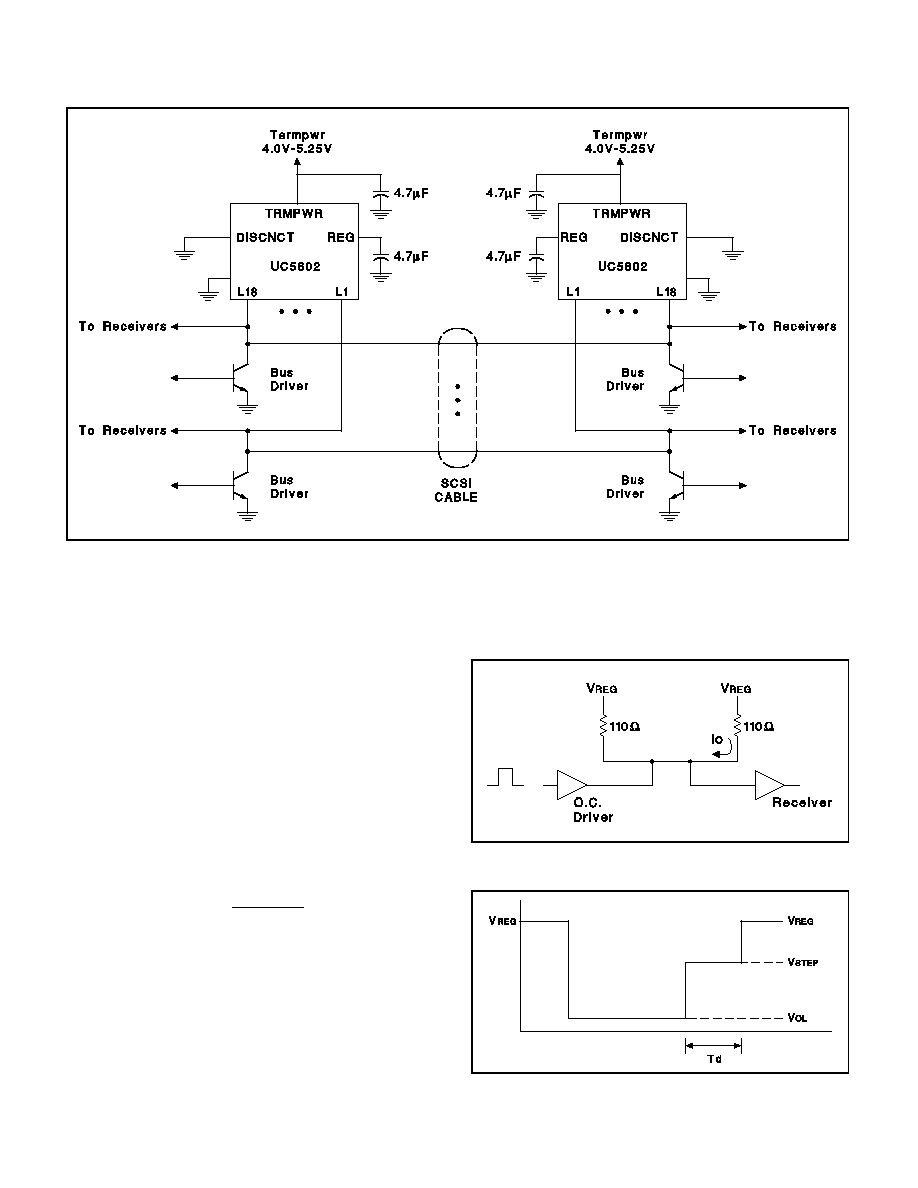
Typical SCSI Bus Configuration Using the UC5602
UC5602
A Look at the Response of a SCSI-2 Cable
Figure 1 shows a single line of a SCSI cable. The driver
is an open colletor type which when asserted pulls low,
and when negated the termination resistance serves as
the pull-up.
Figure 2 shows a worst case scenario of mid cable de-
assertion with a close proximity receiver. The voltage
V
STEP
is defined as:
V
STEP
= V
OL
+I
O
Z
0
V
OL
=
Driver Output Low Voltage
I
O
=
Current from Receiving Terminator
Z
0
=
Cable Characteristic Impedance
I
O
=
V
REG
-
V
OL
110
In the pursuit of higher data rates, sampling could occur
during this step portion, therefore it is important to ensure
that the step is as high as possible to get the most noise
margin. For this reason the UC5602 is trimmed so that
the output current (I
O
) is as close as possible to the SCSI
max current spec of 22.4mA. The Termination impedance
is initially trimmed on the IC to 110 ohms typical, then the
regulator voltage is trimmed for the highest output cur-
rent to within 22.4mA.
Figure 1. A Single Line of a SCSI Cable
Figure 2. A Typical Response of a SCSI Cable
UDG-94054
UDG-94055
UDG-94053
4
UC5602
UNITRODE INTEGRATED CIRCUITS
7 CONTINENTAL BLVD.
∑
∑
MERRIMACK, NH 03054
TEL. (603) 424-241
0 ∑
FAX (603) 424 3460
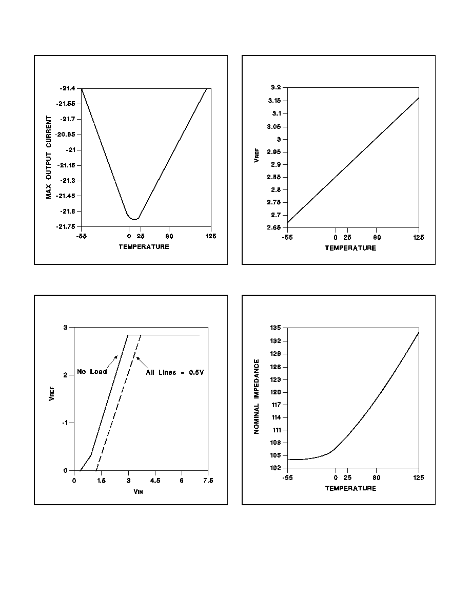
Max Output Current vs. Temperature
V
REF
vs. Temperature
Output Impedance vs. Temperature
V
REF
vs. V
IN
5

IMPORTANT NOTICE
Texas Instruments and its subsidiaries (TI) reserve the right to make changes to their products or to discontinue
any product or service without notice, and advise customers to obtain the latest version of relevant information
to verify, before placing orders, that information being relied on is current and complete. All products are sold
subject to the terms and conditions of sale supplied at the time of order acknowledgement, including those
pertaining to warranty, patent infringement, and limitation of liability.
TI warrants performance of its semiconductor products to the specifications applicable at the time of sale in
accordance with TI's standard warranty. Testing and other quality control techniques are utilized to the extent
TI deems necessary to support this warranty. Specific testing of all parameters of each device is not necessarily
performed, except those mandated by government requirements.
CERTAIN APPLICATIONS USING SEMICONDUCTOR PRODUCTS MAY INVOLVE POTENTIAL RISKS OF
DEATH, PERSONAL INJURY, OR SEVERE PROPERTY OR ENVIRONMENTAL DAMAGE ("CRITICAL
APPLICATIONS"). TI SEMICONDUCTOR PRODUCTS ARE NOT DESIGNED, AUTHORIZED, OR
WARRANTED TO BE SUITABLE FOR USE IN LIFE-SUPPORT DEVICES OR SYSTEMS OR OTHER
CRITICAL APPLICATIONS. INCLUSION OF TI PRODUCTS IN SUCH APPLICATIONS IS UNDERSTOOD TO
BE FULLY AT THE CUSTOMER'S RISK.
In order to minimize risks associated with the customer's applications, adequate design and operating
safeguards must be provided by the customer to minimize inherent or procedural hazards.
TI assumes no liability for applications assistance or customer product design. TI does not warrant or represent
that any license, either express or implied, is granted under any patent right, copyright, mask work right, or other
intellectual property right of TI covering or relating to any combination, machine, or process in which such
semiconductor products or services might be or are used. TI's publication of information regarding any third
party's products or services does not constitute TI's approval, warranty or endorsement thereof.
Copyright
©
1999, Texas Instruments Incorporated