UC5603
9 LINE SCSI ACTIVE TERMINATOR
SLUS195A ≠ MARCH 1997 ≠ REVISED OCTOBER 2000
1
POST OFFICE BOX 655303
∑
DALLAS, TEXAS 75265
D
Complies with SCSI, SCSI≠2 and SPI≠2
Standards
D
6-pF Channel Capacitance during
Disconnect
D
100-
µ
A Supply Current in Disconnect Mode
D
Meets SCSI Hot Plugging
D
≠400-mA Sourcing Current for Termination
D
+400-mA Sinking Current for Active
Negation Drivers
D
Logic Command Disconnects all
Termination Lines
D
Trimmed Termination Current to 3%
D
Trimmed Impedance to 3%
D
Negative Clamping on all Signal Lines
D
Current Limit and Thermal Shutdown
Protection
description
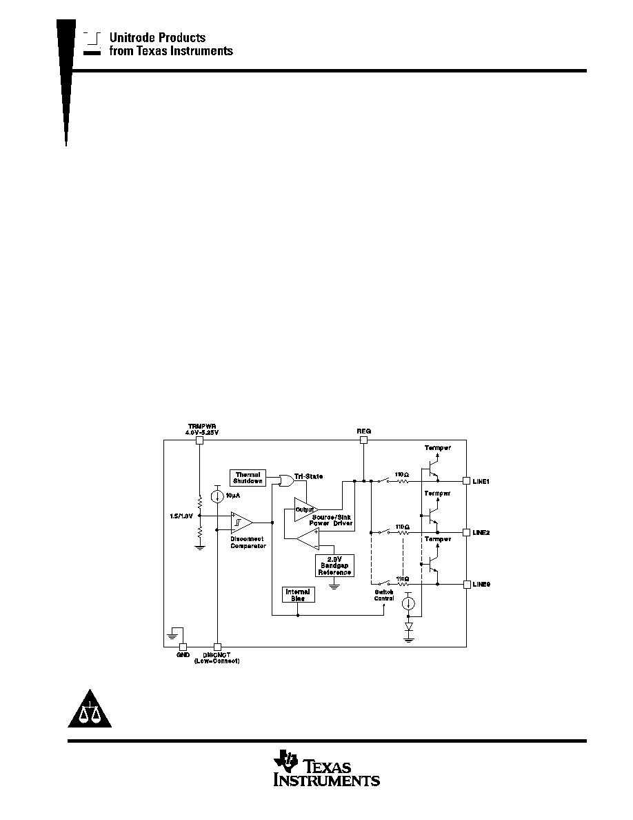
The UC5603 provides 9 lines of active termination for a SCSI (Small Computers Systems Interface) parallel bus.
The SCSI standard recommends active termination at both ends of the cable segment.
The UC5603 provides a disconnect feature which, when opened or driven high, will disconnect all terminating
resistors, and disables the regulator; greatly reducing standby power. The output channels remain high
impedance even without Termpwr applied. A low channel capacitance of 6 pF allows units at interim points of
the bus to have little to no effect on the signal integrity.
Functionally the UC5603 is similar to its predecessor, the UC5601 ≠ 18 line Active Terminator. Several electrical
enhancements were incorporated in the UC5603, such as a sink/source regulator output stage to accommodate
all signal lines at 5 V, while the regulator remains at its nominal value, reduced channel capacitance to 6 pF
typical, and as with the UC5601, custom power packages are utilized to allow normal operation at full power
conditions (1.2 watts).
functional block diagram
UDG-94049
Copyright
©
2000, Texas Instruments Incorporated
PRODUCTION DATA information is current as of publication date.
Products conform to specifications per the terms of Texas Instruments
standard warranty. Production processing does not necessarily include
testing of all parameters.
Please be aware that an important notice concerning availability, standard warranty, and use in critical applications of
Texas Instruments semiconductor products and disclaimers thereto appears at the end of this data sheet.
UC5603
9 LINE SCSI ACTIVE TERMINATOR
SLUS195A ≠ MARCH 1997 ≠ REVISED OCTOBER 2000
2
POST OFFICE BOX 655303
∑
DALLAS, TEXAS 75265
description (continued)
Internal circuit trimming is utilized, first to trim the impedance to a 3% tolerance, and then most importantly, to
trim the output current to a 3% tolerance, as close to the max SCSI spec as possible, which maximizes noise
margin in fast SCSI operation.
Other features include negative clamping on all signal lines to protect external circuitry from latch-up, thermal
shutdown and current limit.
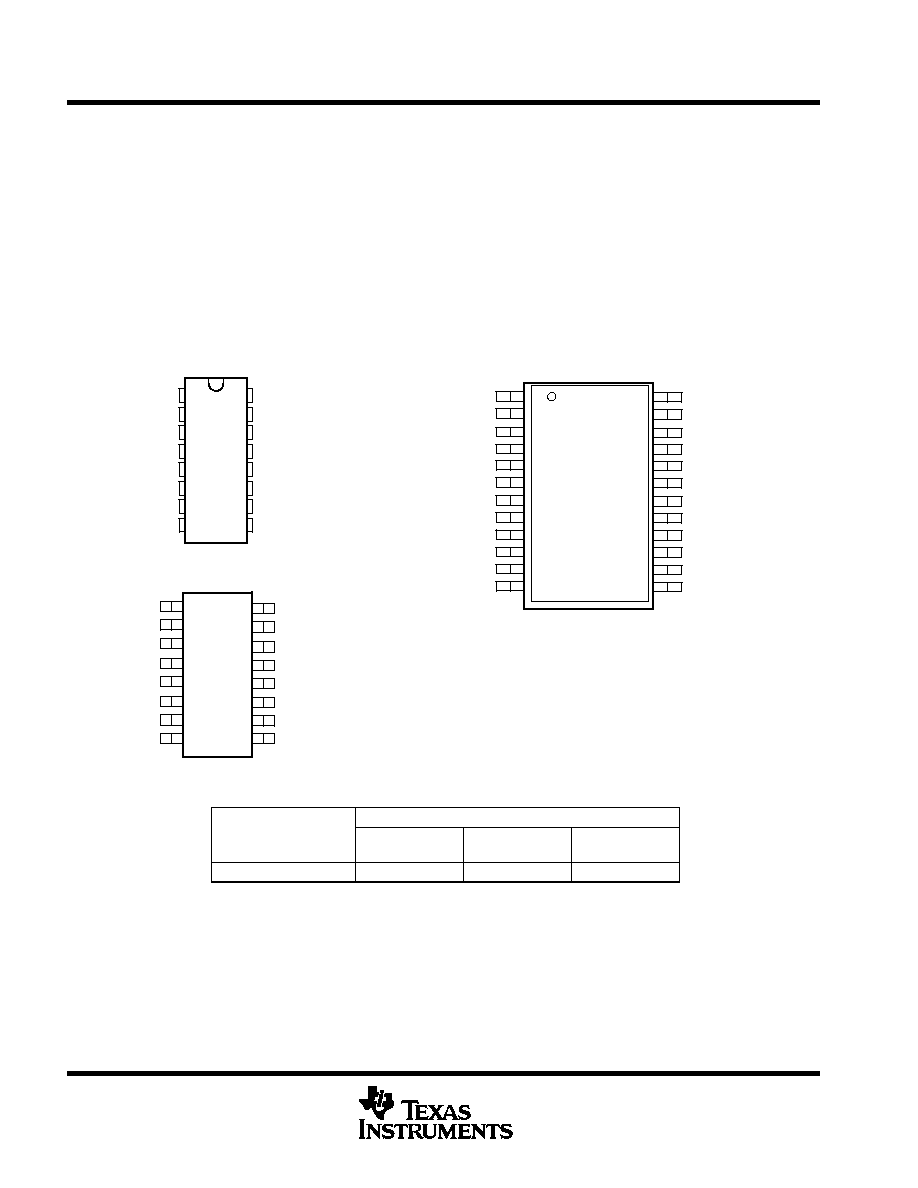
This device is offered in low thermal resistance versions of the industry standard 16 pin narrow body SOIC, and
24 pin TSSOP.
connection diagrams
1
2
3
4
5
6
7
8
9
10
11
12
24
23
22
21
20
19
18
17
16
15
14
13
LINE7
LINE8
LINE9
N/C
SGND
GND*
GND*
GND*
GND*
DISCNCT
LINE1
LINE2
LINE6
LINE5
REG
N/C
GND*
GND*
GND*
GND*
N/C
TRMPR
LINE4
LINE3
PWP PACKAGE
(TOP VIEW)
1
2
3
4
5
6
7
8
16
15
14
13
12
11
10
9
LINE7
LINE8
LINE9
N/C
SGND
DISCNCT
LINE1
LINE2
LINE6
LINE5
REG
N/C
N/C
TRMPWR
LINE4
LINE3
N PACKAGE
(TOP VIEW)
1
2
3
4
5
6
7
8
16
15
14
13
12
11
10
9
DP PACKAGE
(TOP VIEW)
*
PWP package pin 5 serves as signal ground; pins 6,
7, 8, 9, 17, 18, 19, and 20 serve as heatsink/ground.
*
DP package pin 5 serves as signal ground; pins 4,
12, 13 serve as heatsink/ground.
LINE6
LINE5
REG
GND*
GND*
TRMPWR
LINE4
LINE3
LINE7
LINE8
LINE9
GND*
SGND*
DISCNCT
LINE1
LINE2
ORDERING INFORMATION
Packaged Devices
TA = TJ
DIL -16(N)
SOIC-16 (DP)
TSSOP-24
(PWP)
0
∞
C to 70
∞
C
UC5603N
UCUC5603DP
UCUC5603PWP
DP (SOIC≠16) and PWP (TSSOP≠24) packages are available taped and reeled. Add TR
suffix to device type (e.g. UC5603PWPTR) to order quantities of 2000 devices per reel.

UC5603
9 LINE SCSI ACTIVE TERMINATOR
SLUS195A ≠ MARCH 1997 ≠ REVISED OCTOBER 2000
3
POST OFFICE BOX 655303
∑
DALLAS, TEXAS 75265
absolute maximum ratings over operating free-air temperature (unless otherwise noted)
Termpwr voltage
7 V
. . . . . . . . . . . . . . . . . . . . . . . . . . . . . . . . . . . . . . . . . . . . . . . . . . . . . . . . . . . . . . . . . . . . . . . . . . . .
Signal line voltage
0V to 7 V
. . . . . . . . . . . . . . . . . . . . . . . . . . . . . . . . . . . . . . . . . . . . . . . . . . . . . . . . . . . . . . . . . . . . .
Regulator output current
0.5 A
. . . . . . . . . . . . . . . . . . . . . . . . . . . . . . . . . . . . . . . . . . . . . . . . . . . . . . . . . . . . . . . . . . .
Storage temperature
≠65
∞
C to 150
∞
C
. . . . . . . . . . . . . . . . . . . . . . . . . . . . . . . . . . . . . . . . . . . . . . . . . . . . . . . . . . . . .
Operating temperature
≠55
∞
C to 150
∞
C
. . . . . . . . . . . . . . . . . . . . . . . . . . . . . . . . . . . . . . . . . . . . . . . . . . . . . . . . . . .
Lead temperature (soldering, 10 sec.)
300
∞
C
. . . . . . . . . . . . . . . . . . . . . . . . . . . . . . . . . . . . . . . . . . . . . . . . . . . . . .
Stresses beyond those listed under "absolute maximum ratings" may cause permanent damage to the device. These are stress ratings only, and
functional operation of the device at these or any other conditions beyond those indicated under "recommended operating conditions" is not
implied. Exposure to absolute-maximum-rated conditions for extended periods may affect device reliability.
Unless otherwise specified all voltages are with respect to Ground. Currents are positive into, negative out of the specified terminal. Consult
Packaging Section of Unitrode Integrated Circuits databook for thermal limitations and considerations of packages.
recommended operating conditions
Termpwr voltage
3.8 V to 5.25 V
. . . . . . . . . . . . . . . . . . . . . . . . . . . . . . . . . . . . . . . . . . . . . . . . . . . . . . . . . . . . . . . . . .
Signal line voltage
0 V to 5 V
. . . . . . . . . . . . . . . . . . . . . . . . . . . . . . . . . . . . . . . . . . . . . . . . . . . . . . . . . . . . . . . . . . . .
Disconnect input voltage
0 V to Termpwr
. . . . . . . . . . . . . . . . . . . . . . . . . . . . . . . . . . . . . . . . . . . . . . . . . . . . . . . . . . .
electrical characteristics, these specifications apply for T
A
= 0
∞
C to 70
∞
C. TRMPWR = 4.75 V
DISCNCT = 0 V, T
A
= T
J
, (unless otherwise stated)
supply current section
PARAMETER
TEST CONDITIONS
MIN
TYP
MAX
UNITS
Termpwr supply current
All termination lines = Open
12
18
mA
Termpwr supply current
All termination lines = 0.5 V
200
220
mA
Power down mode
DISCNCT = Open
100
150
µ
A
output section (terminator lines)
PARAMETER
TEST CONDITIONS
MIN
TYP
MAX
UNITS
Terminator impedance
ILINE = ≠5 mA to ≠15 mA
107
110
113
Output high voltage
VTRMPWR = 4 V,
See Note 1
2.7
2.9
V
Max output current
V
0 5 V
TJ = 25
∞
C
≠21.1
≠21.9
≠22.4
mA
Max output current
VLINE = 0.5 V
0
∞
C < TJ < 70
∞
C
≠20.5
≠21.9
≠22.4
mA
VLINE = 0.5 V,
TRMPWR = 4 V,
TJ = 25
∞
C
≠20.3
≠21.9
≠22.4
mA
Max output current
VLINE = 0.5 V,
TRMPWR = 4 V,
See Note 1
0
∞
C < TJ < 70
∞
C
≠19.8
≠21.9
≠22.4
mA
Max out ut current
VLINE = 0.2 V,
TRMPWR = 4.0 V to 5.25 V
0
∞
C < TJ < 70
∞
C
≠22.0
≠24.0
≠25.4
mA
Output clamp level
ILINE = ≠30 mA
≠0.2
≠0.05
0.1
V
TRMPWR = 0 V to 5.25,
VLINE = 0 to 4 V
10
400
nA
Output leakage
DISCNCT = 4 V
TRMPWR = 0 V to 5.25,
VREG = 0 V
VLINE = 5.25 V
100
µ
A
Output leakage
DISCNCT = 4 V
TRMPWR = 0 V to 5.25 V,
REG = Open
VLINE = 0 V to 5.25 V
10
400
nA
Output capacitance
DISCNCT = Open
See Note 2
DP Package
6
8
pF
NOTES:
1. Measuring each termination line while other 8 are low (0.5 V).
2. Ensured by design. Not production tested.
UC5603
9 LINE SCSI ACTIVE TERMINATOR
SLUS195A ≠ MARCH 1997 ≠ REVISED OCTOBER 2000
4
POST OFFICE BOX 655303
∑
DALLAS, TEXAS 75265
regulator section
PARAMETER
TEST CONDITIONS
MIN
TYP
MAX
UNITS
Regulator output voltage
2.8
2.9
3
V
Regulator output voltage
All termination lines = 5 V
2.8
2.9
3
V
Line regulation
TRMPWR = 4 V to 6 V
10
20
mV
Load regulation
IREG = 100 mA to ≠100 mA
20
50
mV
Drop out voltage
All termination lines = 0.5 V
0.7
1
V
Short circuit current
VREG = 0 V
≠200
≠400
≠600
mA
Sinking current capability
VREG = 3.5 V
200
400
600
mA
Thermal shutdown
170
∞
C
Thermal shutdown hysteresis
10
∞
C
disconnect section
PARAMETER
TEST CONDITIONS
MIN
TYP
MAX
UNITS
Disconnect threshold
1.3
1.5
1.7
V
Threshold hysteresis
100
160
250
mV
Input current
DISCNCT = 0 V
10
15
mA
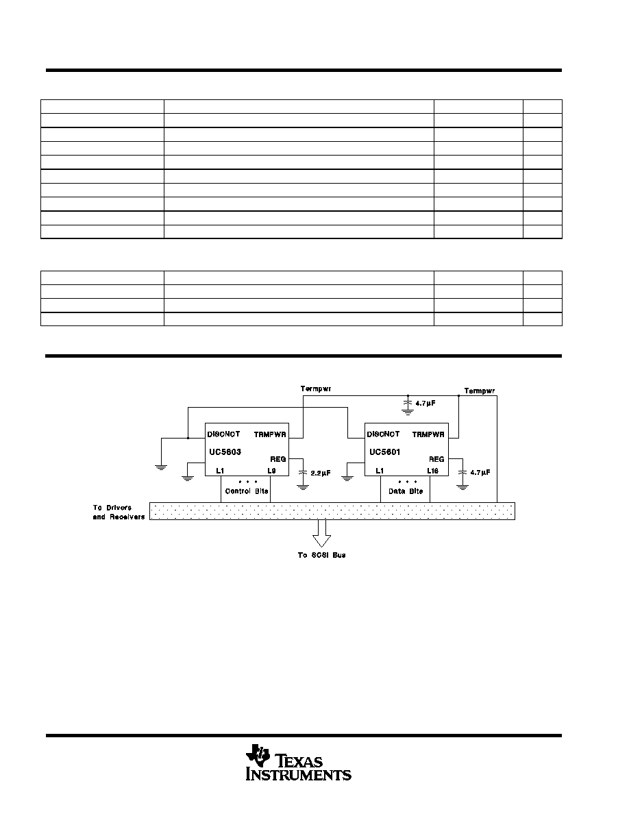
APPLICATION INFORMATION
UDG-94050
Figure 1. Typical Wide SCSI Bus Configurations Utilizing 1 UC5601 and 1 UC5603 Device
UC5603
9 LINE SCSI ACTIVE TERMINATOR
SLUS195A ≠ MARCH 1997 ≠ REVISED OCTOBER 2000
5
POST OFFICE BOX 655303
∑
DALLAS, TEXAS 75265
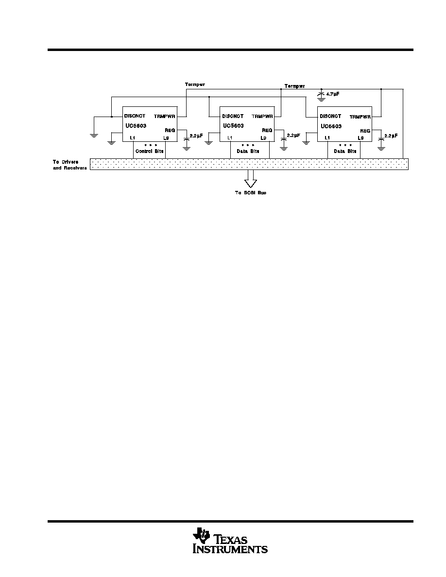
APPLICATION INFORMATION
UDG-94051
Figure 2. Typical Wide SCSI Bus Configurations Utilizing 3 UC5603 Devices

IMPORTANT NOTICE
Texas Instruments and its subsidiaries (TI) reserve the right to make changes to their products or to discontinue
any product or service without notice, and advise customers to obtain the latest version of relevant information
to verify, before placing orders, that information being relied on is current and complete. All products are sold
subject to the terms and conditions of sale supplied at the time of order acknowledgment, including those
pertaining to warranty, patent infringement, and limitation of liability.
TI warrants performance of its semiconductor products to the specifications applicable at the time of sale in
accordance with TI's standard warranty. Testing and other quality control techniques are utilized to the extent
TI deems necessary to support this warranty. Specific testing of all parameters of each device is not necessarily
performed, except those mandated by government requirements.
Customers are responsible for their applications using TI components.
In order to minimize risks associated with the customer's applications, adequate design and operating
safeguards must be provided by the customer to minimize inherent or procedural hazards.
TI assumes no liability for applications assistance or customer product design. TI does not warrant or represent
that any license, either express or implied, is granted under any patent right, copyright, mask work right, or other
intellectual property right of TI covering or relating to any combination, machine, or process in which such
semiconductor products or services might be or are used. TI's publication of information regarding any third
party's products or services does not constitute TI's approval, warranty or endorsement thereof.
Copyright
©
2000, Texas Instruments Incorporated