 | –≠–ª–µ–∫—Ç—Ä–æ–Ω–Ω—ã–π –∫–æ–º–ø–æ–Ω–µ–Ω—Ç: UC5612N | –°–∫–∞—á–∞—Ç—å:  PDF PDF  ZIP ZIP |
UC5612
SLUS164A - MARCH 1997 - REVISED OCTOBER 2003
LOW VOLTAGE DIFFERENTIAL (LVD) SCSI 9 LINE TERMINATOR
1
www.ti.com
FEATURES
D
Complies with SCSI, SCSI-2 and SPI-2
Standards
D
5-pF Channel Capacitance During Disconnect
D
Meets SCSI Hot Plugging
D
-400-mA Sourcing Current for Termination
D
+100-mA Sinking Current for Active Negation
D
1-V Dropout Voltage Regulator
D
Logic High Command Disconnects all
Termination Lines
D
100-
µ
A Supply Current In Disconnect Mode
D
Trimmed Termination Current to 5%
D
Trimmed Impedance to 5%
D
Low Thermal Resistance Surface Mount
Packages
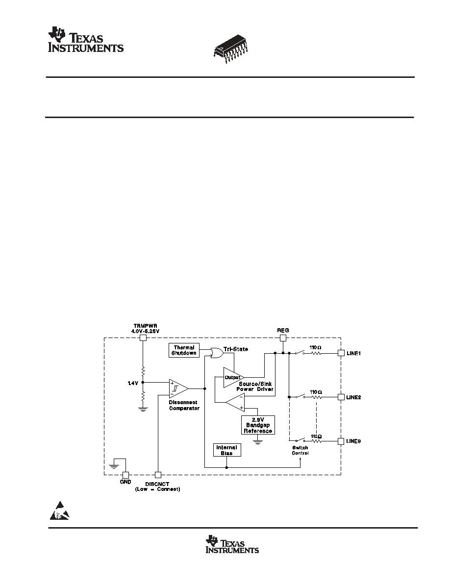
DESCRIPTION
The UC5612 provides 9 lines of active termination for a
small computer systems interface (SCSI) parallel bus.
The SCSI standard recommends active termination at
both ends of the cable segment.
The only functional differences between the UC5603
and UC5612 is the absence of the negative clamps on
the output lines. Parametrically, the UC5612 has a 5%
tolerance on impedance and current compared to a 3%
tolerance on the UC5603. Custom power packages are
utilized to allow normal operation at full power at 2 W.
The UC5612 provides a disconnect feature which,
when opened or driven high, disconnects all terminating
resistors, disables the regulator and greatly reduces
standby power consumption. The output channels
remain high impedance even without TERMPWR
applied. A low channel capacitance of 5 pF allows
interim points of the bus to have little to no effect on the
signal integrity.
BLOCK DIAGRAM
UDG-94133
These devices have limited built-in ESD protection. The leads should be shorted together or the device placed in conductive foam
during storage or handling to prevent electrostatic damage to the MOS gates.
PRODUCTION DATA information is current as of publication date.
Products conform to specifications per the terms of Texas Instruments
standard warranty. Production processing does not necessarily include
testing of all parameters.
Copyright
2003, Texas Instruments Incorporated

UC5612
SLUS164A - MARCH 1997 - REVISED OCTOBER 2003
2
www.ti.com
DESCRIPTION (CONT.)
Internal circuit trimming is utilized, first to trim the impedance to a 5% tolerance, and then most importantly, to
trim the output current to a 5% tolerance, as close to the maximum SCSI specification as possible. This
maximizes the noise margin in fast SCSI operation. Other features include thermal shutdown and current limit.
This device is offered in low thermal resistance versions of the industry standard 16-pin narrow body SOIC,
16-pin DIL and 24-pin TSSOP.
ORDERING INFORMATION
TA
PACKAGED DEVICE
{
PACKAGED DEVICE
{
PACKAGED DEVICE
{
TA
DIL-16 (N)
SOIC-16 (DP)
TSSOP-24 (PWP)
0
∞
C to 70
∞
C
UC5612N
UC5612DP
UC5612PWP
The TSSOP packages are available taped and reeled. Add TR suffix to device type (e.g. UC5612PWPTR) to order quantities
of 2,000 devices per reel.
CONNECTION DIAGRAM
DIL-16 (Top View)
N Package
SOIC-16 (Top View)
DP Package
TSSOP-24 (Top View)
PWP Package
DISCNCT
N/C
N/C
GND*
GND*
LINE6
LINE8
SGND*
GND*
GND*
LINE9
N/C
GND*
LINE7
GND*
LINE1
GND*
GND*
TRMPWR
12
11
10
9
8
7
6
5
4
3
2
1
13
14
15
16
17
18
19
20
21
22
23
24
LINE4
LINE5
REG
LINE2
LINE3
* DP package pin 5 serves as signal
ground; pins 4, 12, and 13 serve as
heatsink/ground.
* PWP package pin 9 serves as signal
ground; pins 5, 6, 7, 8, 17, 18, 19 and
20 serve as heatsink/ground.

UC5612
SLUS164A - MARCH 1997 - REVISED OCTOBER 2003
3
www.ti.com
RECOMMENDED OPERATING CONDITIONS
MIN
NOM
MAX
UNIT
TRMPWR voltage
3.8
5.25
Signal line voltage
0
5.0
V
Disconnect input voltage
0
6.0
V
ABSOLUTE MAXIMUM RATINGS
over operating free-air temperature range unless otherwise noted
{}
UCC5640
UNIT
TRMPWR voltage
7
V
Signal line voltage
0 to 7.0
V
Regulator output current
0.6
A
Storage temperature, Tstg
-65 to 150
Operating junction temperature, TJ
≠55 to 150
∞
C
Lead temperature (soldering, 10 sec.)
300
C
Stresses beyond those listed under "absolute maximum ratings" may cause permanent damage to the device. These are stress ratings only,
and functional operation of the device at these or any other conditions beyond those indicated under "recommended operating conditions" is
not implied. Exposure to absolute-maximum-rated conditions for extended periods may affect device reliability. All voltages are with respect
to GND. Currents are positive into and negative out of, the specified terminal.
Currents are positive into, negative out of the specified terminal. Consult Packaging Section of Databook for thermal limitations and
considerations of packages.

UC5612
SLUS164A - MARCH 1997 - REVISED OCTOBER 2003
4
www.ti.com
ELECTRICAL CHARACTERISTICS
T
A
= 0
∞
C to 70
∞
C, TRMPWR = 4.75 V, T
A
= T
J
, (unless otherwise noted)
PARAMETER
TEST CONDITIONS
MIN
TYP
MAX
UNITS
Supply Current Section
Termpwr supply current
All termination lines = Open
17
23
mA
Termpwr supply current
All termination lines = 0.5 V
200
225
mA
Power down mode
DISCNCT = Open
100
150
µ
A
Output Section (Termination Lines)
Terminator impedance
ILINE = -5 mA to -15 mA
104.5
110
115.5
Output high voltage
2.65
2.9
3.1
V
Max output current
VLINE = 0.5 V
TJ = 25
∞
C
-20.3
-21.5
-22.4
Max output current
VLINE = 0.5 V
0
∞
C < TJ < 70
∞
C
-19.8
-21.5
-22.4
VLINE = 0.5 V, TRMPWR = 4 V (1)
TJ = 25
∞
C
-19.5
-21.5
-22.4
mA
Max output current
VLINE = 0.5 V, TRMPWR = 4 V (1)
0
∞
C < TJ < 70
∞
C
-19.0
-21.5
-22.4
mA
Max output current
VLINE = 0.2V,
TRMPWR = 4 V to 5.25 V
0
∞
C < TJ < 70
∞
C
-21.6
-24.0
-25.4
DISCNCT = 4 V,
REG = 0 V,
VLINE = 0 V to 4 V
10
400
nA
Output leakage
DISCNCT = 4 V,
REG = 0 V,
TRMPWR = 0 V to 5.25 V
VLINE = 5.25 V
100
µ
A
Output leakage
REG = Open
VLINE = 0 V to 5.25 V
10
400
nA
Output capacitance
DISCNCT = Open, (DP package)(2)
5
6
pF
Regulator Section
Regulator output voltage
2.7
2.9
3.1
V
Regulator output voltage
All termination lines = 4 V
2.7
2.9
3.1
V
Line regulation
TRMPWR = 4 V to 6 V
10
20
mV
Drop out voltage
All termination lines = 0.5 V
1.0
1.2
V
Short circuit current
REG = 0 V
-200
-400
-600
mA
Sinking current capability
REG = 3.5 V
75
100
400
mA
Thermal shutdown
170
∞
C
Thermal shutdown hysteresis
10
∞
C
Disconnect Section
Disconnect threshold
1.1
1.4
1.7
V
Input current
DISCNCT = 0 V
-10
-20
µ
A
NOTE:
(1) Measuring each termination line while other eight are low.
(2) Ensured by design. Not production tested.
TERMINAL FUNCTIONS
(1)
TERMINAL
I/O
DESCRIPTION
NAME
NO.
I/O
DESCRIPTION
DISCNCT
6
Taking this pin high or leaving it open causes the nine channels to become
high impedance and the chip to go into low-power mode; a low state allows the
channels to provide normal termination.
GND
5
Ground reference for the device
LINE1 - LINE9
1, 2, 3, 7, 8, 9,
10, 15, 16
110-
termination channels.
REG
14
Output of the internal 2.8-V regulator.
TRMPWR
11
Power for the device.
NOTE:
(1) N package.
UC5612
SLUS164A - MARCH 1997 - REVISED OCTOBER 2003
5
www.ti.com
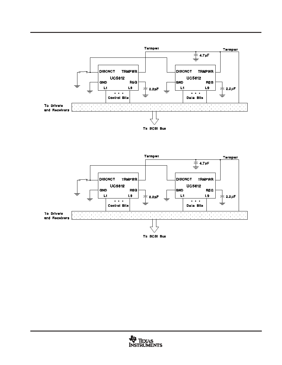
APPLICATION INFORMATION
UDG-94134
Figure 1. Typical SCSI Bus Configurations Utilizing Two UC5612 Devices
UDG-94135
Figure 2. Typical Wide SCSI Bus Configurations Utilizing Three UC5612 Devices

UC5612
SLUS164A - MARCH 1997 - REVISED OCTOBER 2003
6
www.ti.com
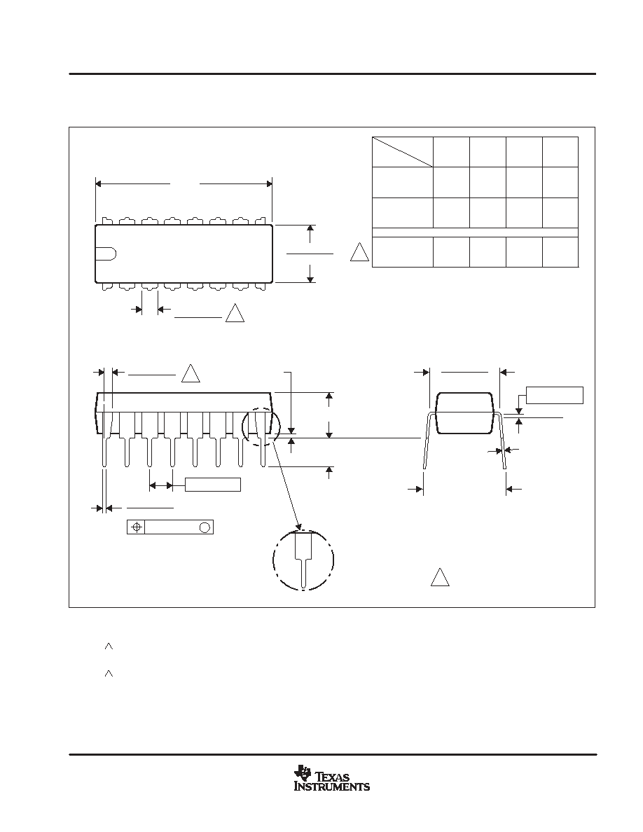
MECHANICAL DATA
D (R-PDSO-G**)
PLASTIC SMALL-OUTLINE PACKAGE
8 PINS SHOWN
8
0.197
(5,00)
A MAX
A MIN
(4,80)
0.189
0.337
(8,55)
(8,75)
0.344
14
0.386
(9,80)
(10,00)
0.394
16
DIM
PINS **
4040047/E 09/01
0.069 (1,75) MAX
Seating Plane
0.004 (0,10)
0.010 (0,25)
0.010 (0,25)
0.016 (0,40)
0.044 (1,12)
0.244 (6,20)
0.228 (5,80)
0.020 (0,51)
0.014 (0,35)
1
4
8
5
0.150 (3,81)
0.157 (4,00)
0.008 (0,20) NOM
0
∞
- 8
∞
Gage Plane
A
0.004 (0,10)
0.010 (0,25)
0.050 (1,27)
NOTES: A. All linear dimensions are in inches (millimeters).
B. This drawing is subject to change without notice.
C. Body dimensions do not include mold flash or protrusion, not to exceed 0.006 (0,15).
D. Falls within JEDEC MS-012
MECHANICAL
MPDI002C - JANUARY 1995 - REVISED DECEMBER 20002
7
www.ti.com
MECHANICAL DATA
N (R-PDIP-T**)
PLASTIC DUAL-IN-LINE PACKAGE
BB
AC
AD
0.325 (8,26)
0.300 (7,62)
0.010 (0,25) NOM
Gauge Plane
0.015 (0,38)
0.430 (10,92) MAX
20
1.060
(26,92)
0.940
(23,88)
18
0.920
0.850
14
0.775
0.745
(19,69)
(18,92)
16
0.775
(19,69)
(18,92)
0.745
A MIN
DIM
A MAX
PINS **
(23,37)
(21,59)
Seating Plane
14/18 PIN ONLY
20 pin vendor option
4040049/E 12/2002
9
8
0.070 (1,78)
A
0.045 (1,14)
0.020 (0,51) MIN
16
1
0.015 (0,38)
0.021 (0,53)
0.200 (5,08) MAX
0.125 (3,18) MIN
0.240 (6,10)
0.260 (6,60)
M
0.010 (0,25)
0.100 (2,54)
16 PINS SHOWN
MS-100
VARIATION
AA
C
D
D
D
0.030 (0,76)
0.045 (1,14)
NOTES: A. All linear dimensions are in inches (millimeters).
B. This drawing is subject to change without notice.
C. Falls within JEDEC MS-001, except 18 and 20 pin
minimum body lrngth (Dim A).
D. The 20 pin end lead shoulder width is a vendor option,
either half or full width.
MECHANICAL
MPDI002C - JANUARY 1995 - REVISED DECEMBER 20002
8
www.ti.com
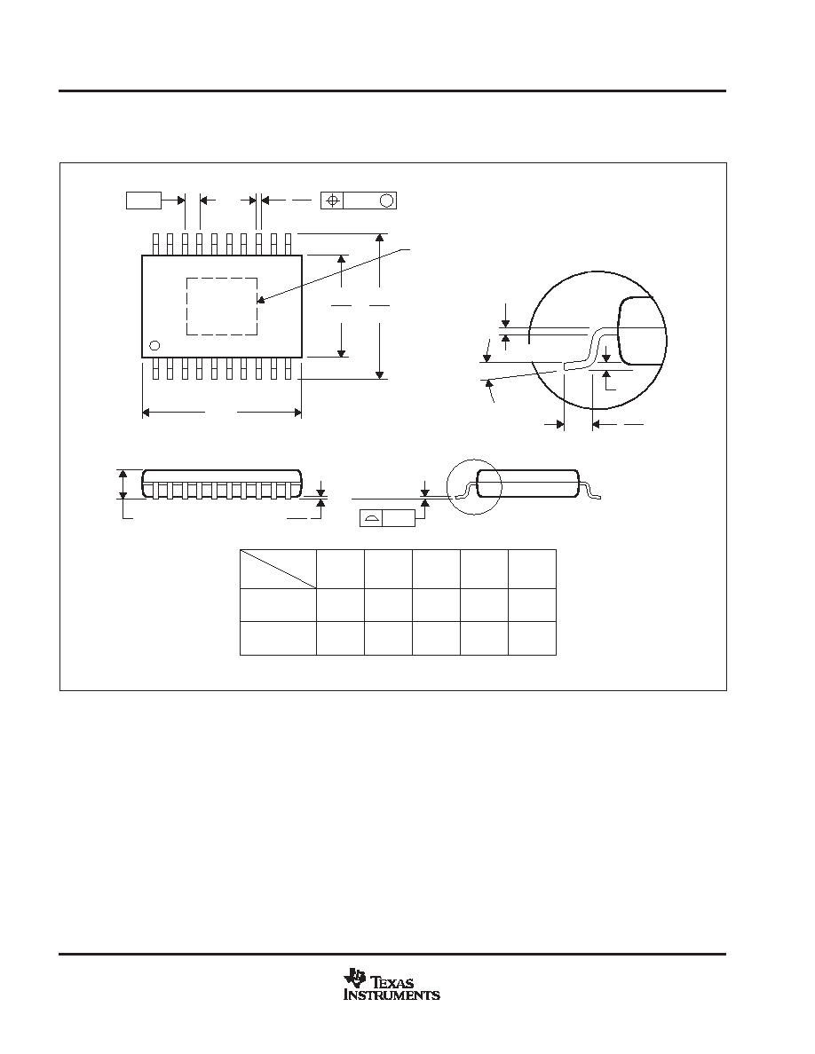
MECHANICAL DATA
PWP (R-PDSO-G**)
PowerPAD
PLASTIC SMALL-OUTLINE
4073225/F 10/98
0,50
0,75
0,25
0,15 NOM
Thermal Pad
(See Note D)
Gage Plane
28
24
7,70
7,90
20
6,40
6,60
9,60
9,80
6,60
6,20
11
0,19
4,50
4,30
10
0,15
20
A
1
0,30
1,20 MAX
16
14
5,10
4,90
PINS **
4,90
5,10
DIM
A MIN
A MAX
0,05
Seating Plane
0,65
0,10
M
0,10
0
∞
- 8
∞
20 PINS SHOWN
NOTES: E. All linear dimensions are in millimeters.
F. This drawing is subject to change without notice.
G. Body dimensions do not include mold flash or protrusions.
H. The package thermal performance may be enhanced by bonding the thermal pad to an external thermal plane.
This pad is electrically and thermally connected to the backside of the die and possibly selected leads.
I. Falls within JEDEC MO-153

IMPORTANT NOTICE
Texas Instruments Incorporated and its subsidiaries (TI) reserve the right to make corrections, modifications,
enhancements, improvements, and other changes to its products and services at any time and to discontinue
any product or service without notice. Customers should obtain the latest relevant information before placing
orders and should verify that such information is current and complete. All products are sold subject to TI's terms
and conditions of sale supplied at the time of order acknowledgment.
TI warrants performance of its hardware products to the specifications applicable at the time of sale in
accordance with TI's standard warranty. Testing and other quality control techniques are used to the extent TI
deems necessary to support this warranty. Except where mandated by government requirements, testing of all
parameters of each product is not necessarily performed.
TI assumes no liability for applications assistance or customer product design. Customers are responsible for
their products and applications using TI components. To minimize the risks associated with customer products
and applications, customers should provide adequate design and operating safeguards.
TI does not warrant or represent that any license, either express or implied, is granted under any TI patent right,
copyright, mask work right, or other TI intellectual property right relating to any combination, machine, or process
in which TI products or services are used. Information published by TI regarding third-party products or services
does not constitute a license from TI to use such products or services or a warranty or endorsement thereof.
Use of such information may require a license from a third party under the patents or other intellectual property
of the third party, or a license from TI under the patents or other intellectual property of TI.
Reproduction of information in TI data books or data sheets is permissible only if reproduction is without
alteration and is accompanied by all associated warranties, conditions, limitations, and notices. Reproduction
of this information with alteration is an unfair and deceptive business practice. TI is not responsible or liable for
such altered documentation.
Resale of TI products or services with statements different from or beyond the parameters stated by TI for that
product or service voids all express and any implied warranties for the associated TI product or service and
is an unfair and deceptive business practice. TI is not responsible or liable for any such statements.
Following are URLs where you can obtain information on other Texas Instruments products and application
solutions:
Products
Applications
Amplifiers
amplifier.ti.com
Audio
www.ti.com/audio
Data Converters
dataconverter.ti.com
Automotive
www.ti.com/automotive
DSP
dsp.ti.com
Broadband
www.ti.com/broadband
Interface
interface.ti.com
Digital Control
www.ti.com/digitalcontrol
Logic
logic.ti.com
Military
www.ti.com/military
Power Mgmt
power.ti.com
Optical Networking
www.ti.com/opticalnetwork
Microcontrollers
microcontroller.ti.com
Security
www.ti.com/security
Telephony
www.ti.com/telephony
Video & Imaging
www.ti.com/video
Wireless
www.ti.com/wireless
Mailing Address:
Texas Instruments
Post Office Box 655303 Dallas, Texas 75265
Copyright
2003, Texas Instruments Incorporated