 | –≠–ª–µ–∫—Ç—Ä–æ–Ω–Ω—ã–π –∫–æ–º–ø–æ–Ω–µ–Ω—Ç: UCC1808-1 | –°–∫–∞—á–∞—Ç—å:  PDF PDF  ZIP ZIP |
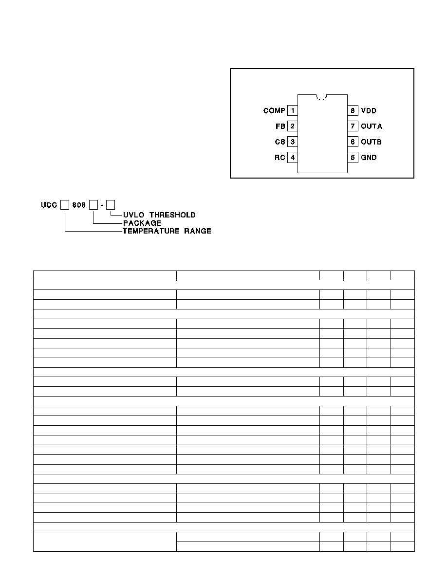
UCC1808-1/-2
UCC2808-1/-2
UCC3808-1/-2
04/99
FEATURES
∑
130
µ
A Typical Starting Current
∑
1mA Typical Run Current
∑
Operation to 1MHz
∑
Internal Soft Start
∑
On Chip Error Amplifier With 2MHz
Gain Bandwidth Product
∑
On Chip VDD Clamping
∑
Dual Output Drive Stages In Push-Pull
Configuration
∑
Output Drive Stages Capable Of
500mA Peak Source Current, 1A
Peak Sink Current
Low Power Current Mode Push-Pull PWM
3
1
2
8
7
6
5
4
OSCILLATOR
S
Q
R
0.8V
RC
1.2R
R
0.5V
PEAK CURRENT
COMPARATOR
Q
Q
T
S
Q
R
S
Q
R
VDD
VOLTAGE
REFERENCE
14V
PWM
COMPARATOR
PWM
LATCH
SOFT START
0.5V
VDD≠1V
0.75V
2.2V
2.0V
FB
COMP
CS
VDD
OUTA
OUTB
GND
SLOPE = 1V/ms
VDD OK
OVERCURRENT
COMPARATOR
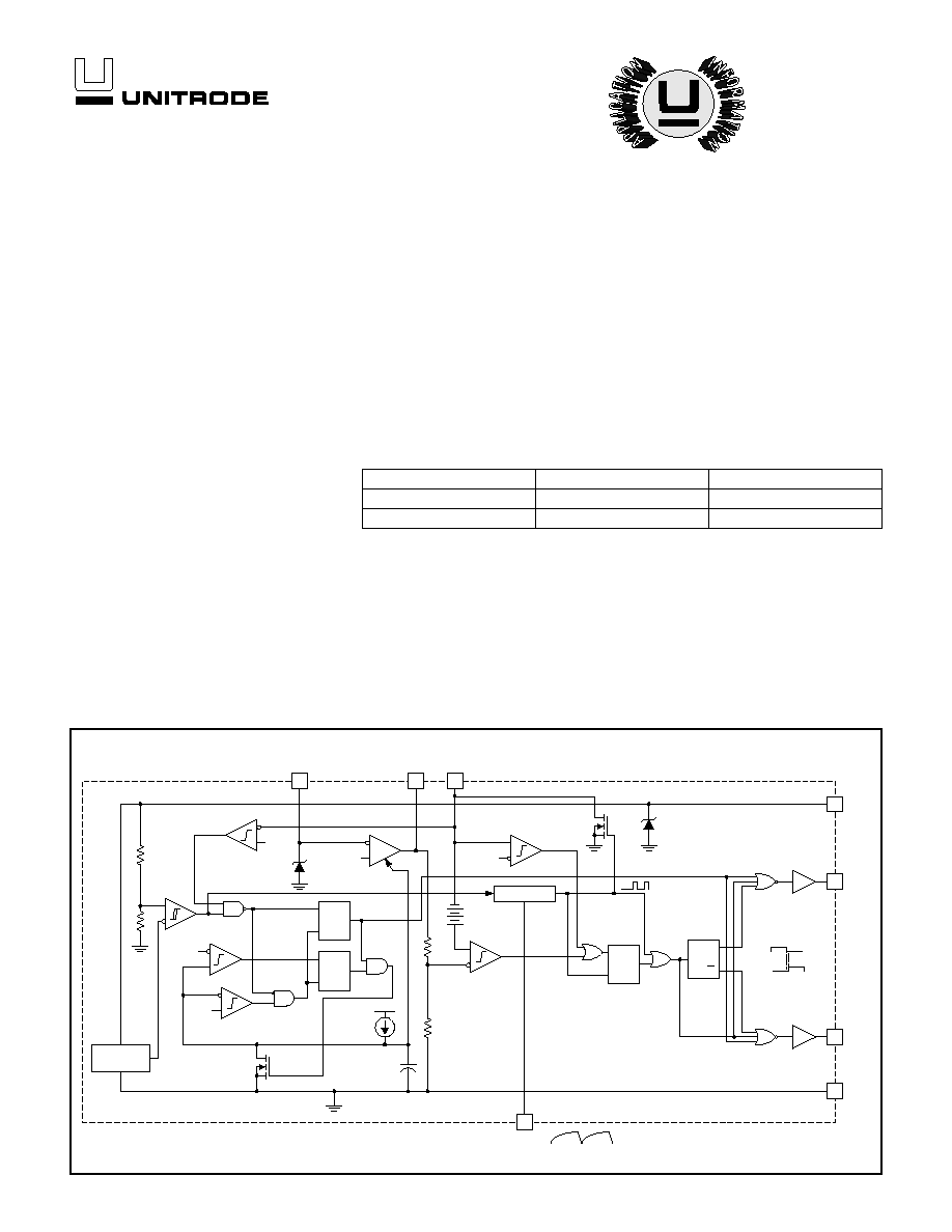
BLOCK DIAGRAM
UDG-99076
DESCRIPTION
The UCC3808 is a family of BiCMOS push-pull, high-speed, low power,
pulse width modulators. The UCC3808 contains all of the control and drive
circuitry required for off-line or DC-to-DC fixed frequency current-mode
switching power supplies with minimal external parts count.
The UCC3808 dual output drive stages are arranged in a push-pull configu-
ration. Both outputs switch at half the oscillator frequency using a toggle
flip-flop. The dead time between the two outputs is typically 60ns to 200ns
depending on the values of the timing capacitor and resistors, thus limits
each output stage duty cycle to less than 50%.
The UCC3808 family offers a variety of package options temperature range
options, and choice of undervoltage lockout levels. The family has UVLO
thresholds and hysteresis options for off-line and battery powered systems.
Thresholds are shown in the table below.
Part Number
Turn on Threshold
Turn off Threshold
UCCx808-1
12.5V
8.3V
UCCx808-2
4.3V
4.1V
2
UCC1808-1/-2
UCC2808-1/-2
UCC3808-1/-2
CONNECTION DIAGRAM
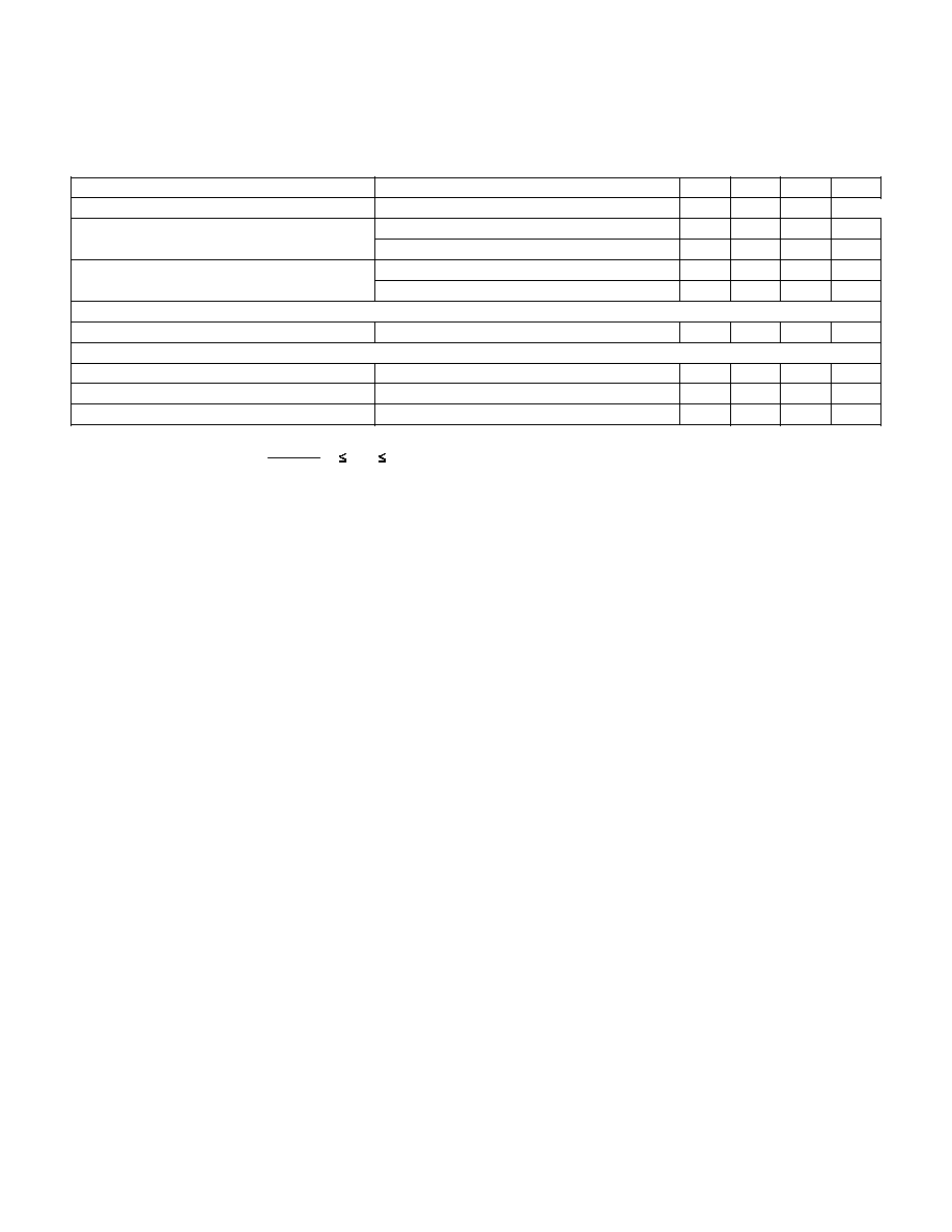
ELECTRICAL CHARACTERISTICS:
Unless otherwise specified,T
A
= 0∞C to 70∞C for the UCC3808-X, ≠40∞C to 85∞C for
the UCC2808-X and ≠55∞C to 125∞C for the UCC1808-X, VDD = 10V (Note 6), 1
µ
F capacitor from VDD to GND, R = 22k
,
C = 330pF. T
A
= T
J
.
PARAMETER
TEST CONDITIONS
MIN
TYP
MAX
UNITS
Oscillator Section
Oscillator Frequency
175
194
213
kHz
Oscillator Amplitude/VDD
(Note 1)
0.44
0.5
0.56
V/V
Error Amplifier Section
Input Voltage
COMP = 2V
1.95
2
2.05
V
Input Bias Current
≠1
1
µ
A
Open Loop Voltage Gain
60
80
dB
COMP Sink Current
FB = 2.2V, COMP = 1V
0.3
2.5
mA
COMP Source Current
FB = 1.3V, COMP = 3.5V
≠0.2
≠0.5
mA
PWM Section
Maximum Duty Cycle
Measured at OUTA or OUTB
48
49
50
%
Minimum Duty Cycle
COMP = 0V
0
%
Current Sense Section
Gain
(Note 2)
1.9
2.2
2.5
V/V
Maximum Input Signal
COMP = 5V (Note 3)
0.45
0.5
0.55
V
CS to Output Delay
COMP = 3.5V, CS from 0 to 600mV
100
200
ns
CS Source Current
≠200
nA
CS Sink Current
CS = 0.5V, RC = 5.5V (Note 7)
5
10
mA
Over Current Threshold
0.7
0.75
0.8
V
COMP to CS Offset
CS = 0V
0.35
0.8
1.2
V
Output Section
OUT Low Level
I = 100mA
0.5
1
V
OUT High Level
I = ≠50mA, VDD ≠ OUT
0.5
1
V
Rise Time
C
L
= 1nF
25
60
ns
Fall Time
C
L
= 1nF
25
60
ns
Undervoltage Lockout Section
Start Threshold
UCCx808-1 (Note 6)
11.5
12.5
13.5
V
UCCx808-2
4.1
4.3
4.5
V
DIL-8, SOIC-8 (Top View)
J or N Package, D Package
Supply Voltage (IDD
10mA) . . . . . . . . . . . . . . . . . . . . . . . 15V
Supply Current . . . . . . . . . . . . . . . . . . . . . . . . . . . . . . . . . 20mA
OUTA/OUTB Source Current (peak) . . . . . . . . . . . . . . . . ≠0.5A
OUTA/OUTB Sink Current (peak) . . . . . . . . . . . . . . . . . . . 1.0A
Analog Inputs (FB, CS) . ≠0.3V to VDD+0.3V, not to exceed 6V
Power Dissipation at T
A
= 25∞C (N Package). . . . . . . . . . . . 1W
Power Dissipation at T
A
= 25∞C (D Package) . . . . . . . . 650mW
Storage Temperature . . . . . . . . . . . . . . . . . . . ≠65∞C to +150∞C
Junction Temperature . . . . . . . . . . . . . . . . . . . ≠55∞C to +150∞C
Lead Temperature (Soldering, 10sec.) . . . . . . . . . . . . . +300∞C
Currents are positive into, negative out of the specified terminal.
Consult Packaging Section of Databook for thermal limitations
and considerations of package.
ABSOLUTE MAXIMUM RATINGS
ORDER INFORMATION
3
UCC1808-1/-2
UCC2808-1/-2
UCC3808-1/-2
ELECTRICAL CHARACTERISTICS:
Unless otherwise specified,T
A
= 0∞C to 70∞C for the UCC3808-X, ≠40∞C to 85∞C for
the UCC2808-X and ≠55∞C to 125∞C for the UCC1808-X, VDD = 10V (Note 6), 1
µ
F capacitor from VDD to GND, R = 22k
,
C = 330pF. T
A
= T
J
.
PARAMETER
TEST CONDITIONS
MIN
TYP
MAX
UNITS
Undervoltage Lockout Section (cont.)
Minimum Operating Voltage After Start
UCCx808-1
7.6
8.3
9
V
UCCx808-2
3.9
4.1
4.3
V
Hysteresis
UCCx808-1
3.5
4.2
5.1
V
UCCx808-2
0.1
0.2
0.3
V
Soft Start Section
COMP Rise Time
FB = 1.8V, Rise from 0.5V to 4V
3.5
20
ms
Overall Section
Startup Current
VDD < Start Threshold
130
260
µ
A
Operating Supply Current
FB = 0V, CS = 0V (Note 5 and 6)
1
2
mA
VDD Zener Shunt Voltage
IDD = 10mA (Note 4)
13
14
15
V
Note 1: Measured at RC. Signal amplitude tracks VDD.
Note 2: Gain is defined by A
V
V
COMP
CS
=
, 0
V
CS
0.4V.
Note 3: Parameter measured at trip point of latch with FB at 0V.
Note 4: Start threshold and Zener Shunt threshold track one another.
Note 5: Does not include current in the external oscillator network.
Note 6: For UCCx808-1, set VDD above the start threshold before setting at 10V.
Note 7: The internal current sink on the CS pin is designed to discharge an external filter capacitor. It is not intended to be a DC
sink path.
COMP: COMP is the output of the error amplifier and the
input of the PWM comparator. The error amplifier in the
UCC3808 is a true low-output impedance, 2MHz opera-
tional amplifier. As such, the COMP pin can both source
and sink current. However, the error amplifier is internally
current limited, so that zero duty cycle can be externally
forced by pulling COMP to GND.
The UCC3808 family features built-in full cycle soft start.
Soft start is implemented as a clamp on the maximum
COMP voltage.
CS: The input to the PWM,
peak current, and
overcurrent comparators. The overcurrent comparator is
only
intended
for
fault
sensing.
Exceeding
the
overcurrent threshold will cause a soft start cycle. An in-
ternal MOSFET discharges the current sense filter ca-
pacitor to improve dynamic performance of the power
converter.
FB: The inverting input to the error amplifier. For best
stability, keep FB lead length as short as possible and FB
stray capacitance as small as possible.
GND: Reference ground and power ground for all func-
tions. Due to high currents, and high frequency operation
of the UCC3808, a low impedance circuit board ground
plane is highly recommended.
OUTA and OUTB: Alternating high current output
stages. Both stages are capable of driving the gate of a
power MOSFET. Each stage is capable of 500mA peak
source current, and 1A peak sink current.
The output stages switch at half the oscillator frequency,
in a push/pull configuration. When the voltage on the RC
pin is rising, one of the two outputs is high, but during fall
time, both outputs are off. This "dead time" between the
two outputs, along with a slower output rise time than fall
time, insures that the two outputs can not be on at the
same time. This dead time is typically 60ns to 200ns and
depends upon the values of the timing capacitor and re-
sistor.
The high-current output drivers consist of MOSFET out-
put devices, which switch from VDD to GND. Each out-
put stage also provides a very low impedance to
overshoot and undershoot. This means that in many
cases, external schottky clamp diodes are not required.
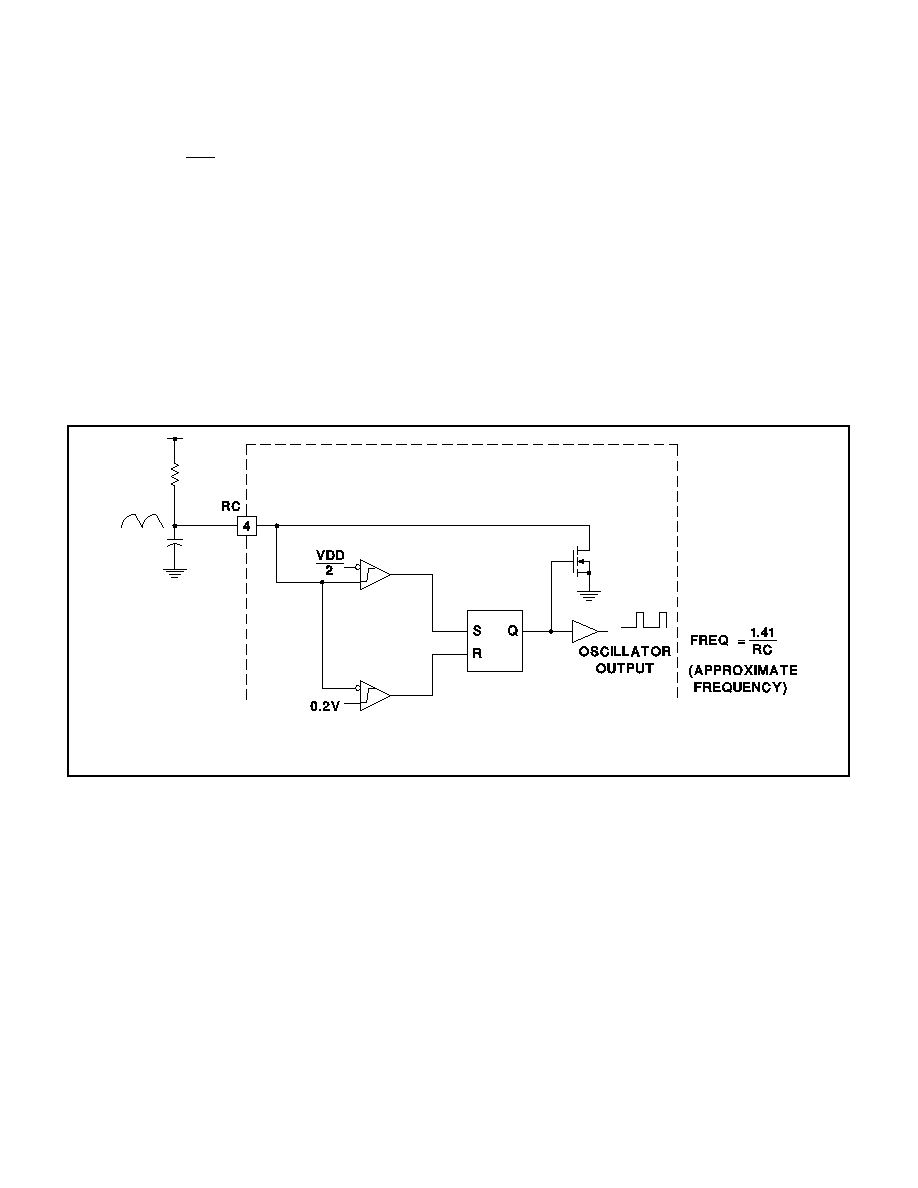
RC: The oscillator programming pin. The UCC3808's os-
cillator tracks VDD and GND internally, so that variations
in power supply rails minimally affect frequency stability.
Fig. 1 shows the oscillator block diagram.
Only two components are required to program the oscil-
lator, a resistor (tied to the VDD and RC), and a capaci-
tor (tied to the RC and GND). The approximate oscillator
frequency is determined by the simple formula:
PIN DESCRIPTIONS
4
UCC1808-1/-2
UCC2808-1/-2
UCC3808-1/-2
f
RC
OSCILLATOR
=
1 41
.
where frequency is in Hertz, resistance in Ohms, and ca-
pacitance in Farads. The recommended range of timing
resistors is between 10k
and 200k
and range of tim-
ing capacitors is between 100pF and 1000pF. Timing re-
sistors less than 10k
should be avoided.
For best performance, keep the timing capacitor lead to
GND as short as possible, the timing resistor lead from
VDD as short as possible, and the leads between timing
components and RC as short as possible. Separate
ground and VDD traces to the external timing network
are encouraged.
VDD: The power input connection for this device. Al-
though quiescent VDD current is very low, total supply
current will be higher, depending on OUTA and OUTB
current, and the programmed oscillator frequency. Total
VDD current is the sum of quiescent VDD current and
the average OUT current. Knowing the operating fre-
quency and the MOSFET gate charge (Qg), average
OUT current can be calculated from
I
OUT
= Qg ∑ F, where F is frequency.
To prevent noise problems, bypass VDD to GND with a
ceramic capacitor as close to the chip as possible along
with an electrolytic capacitor. A 1
µ
F decoupling capacitor
is recommended.
PIN DESCRIPTIONS (cont.)
The oscillator generates a sawtooth waveform on RC. During the RC rise time, the output stages alternate on time, but both
stages are off during the RC fall time. The output stages switch a Ω the oscillator frequency, with guaranteed duty cycle of <
50% for both outputs.
Figure 1. Block diagram for oscillator.
UDG-97009
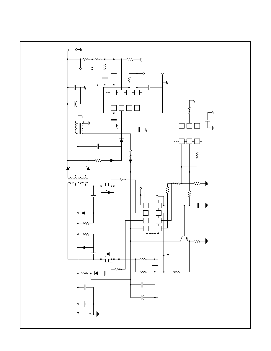
A 200kHz push-pull application circuit with a full wave rec-
tifier is shown in Fig. 2. The output, V
O
, provides 5V at
75W maximum and is electrically isolated from the input.
Since the UCC3808 is a peak current mode controller the
2N2222A emitter following amplifier (buffers the CT wave-
form) provides slope compensation which is necessary
for duty ratios greater than 50%. Capacitor decoupling is
very important with a single ground IC controller and a
1
µ
F is suggested as close to the IC as possible. The con-
troller supply is a series RC for startup, paralleled with a
bias winding on the output inductor used in steady state
operation.
Isolation is provided by an optocoupler with regulation
done on the secondary side using the UC3965 Precision
Reference with Low Offset Error Amplifier. Small signal
compensation with tight voltage regulation is achieved
using this part on the secondary side. Many choices ex-
ist for the output inductor depending on cost, volume,
and mechanically strength. Several design options are
iron powder, molypermalloy (MPP), or a ferrite core with
an air gap as shown here. The main power transformer
is a low profile design, EFD size 25, using Magnetics
Inc. P material which is a good choice at this frequency
and temperature. The input voltage may range from 36V
dc to 72V dc. Refer to application note U-170 for addi-
tion design information.
APPLICATION INFORMATION
5
UCC1808-1/-2
UCC2808-1/-2
UCC3808-1/-2
Figure 2. Typical application diagram.
APPLICATION INFORMATION (cont.)
UDG-97010-1
U
C
C
3808D
-
1
RC
4.99k
4.99k
432
0.1
µ
F
47
µ
F
2N
2222A
20k
330pF
97.6k
2k
301k
0.01
µ
F
1kV
10
2.7
N
S1
N
S2
N
P1
N
P2
1.0
µ
F
EF
25
8:24
680
µ
F
0.01
µ
F
10k
1.0
µ
F
390pF
1.0
µ
F
4700pF
21.0k
26.1k
COM
P
26.1k
49.9k
LOOP
B
LOOP
A
1N
4148
1N
4148
2.2
0.05
2k
330pF
1000pF
62
62
1000pF
2.2
56k
1N
5244
14V
0.47
µ
F
4700
µ
F
V
IN
36V
T
O
72V
+
≠
BYV
28-
200
BYV
28-
200
32C
T
Q
030
EFD
2
5
10:2
+
V
O
5V
75W
CLOSED-LOOP
SOFT-STAR
T
S
E
C
ONDA
RY
GROUND
5
6
7
8
4
3
2
1
MOC
8102
4
5
6
3
2
1
U3
CURRE
NT
SEN
SE
PR
IMAR
Y
GROUND
1N
4148
U1
1
2
3
4
8
7
6
5
U
C
3965D
P
100pF
≠
(OPTI
O
NAL
)
IR
F
640
IR
F
640
866