 | –≠–ª–µ–∫—Ç—Ä–æ–Ω–Ω—ã–π –∫–æ–º–ø–æ–Ω–µ–Ω—Ç: UCC18502 | –°–∫–∞—á–∞—Ç—å:  PDF PDF  ZIP ZIP |
UCC18500/1/2/3
UCC28500/1/2/3
UCC38500/1/2/3
PRELIMINARY
DESCRIPTION
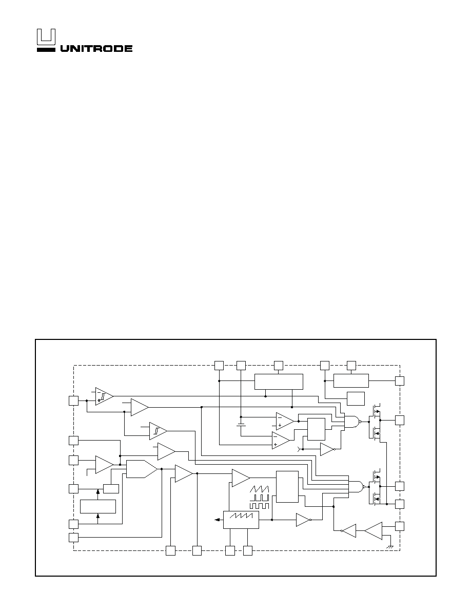
The UCC18500 family provides all of the functions necessary for an ac-
tive power factor corrected preregulator and a second stage DC-to-DC
converter. The controller achieves near-unity power factor by shaping
the AC input line current waveform to correspond to the AC input line
voltage using average current mode control. The DC-to-DC converter
uses peak current mode control to perform the step down power con-
version.
The PFC stage is leading edge modulated while the second stage is
trailing edge synchronized to allow for minimum overlap between the
boost and PWM switches. This reduces ripple current in the bulk output
capacitor.
In order to operate with a three to one range of input line voltages, a
line feedforward (V
FF
) in used to keep input power constant with vary-
ing input voltage. Generation of V
FF
is done using I
AC
in conjunction
with an external single pole filter. This not only reduces external parts
count, but avoids the use of high voltage components offering a lower
cost solution. The multiplier then divides the line current by the square
of V
FF
.
(continued)
BiCMOS PFC/PWM Combination Controller
FEATURES
∑
Combines PFC and 2
nd
Stage Down
Converter Function
∑
Controls Boost PWM to Near-unity Power
Factor
∑
Accurate Power Limiting
∑
Average Current Mode Control in PFC
Stage
∑
Peak Current Mode Control in Second
Stage
∑
Programmable Oscillator
∑
Leading Edge/Trailing Edge Modulation
for Reduced Output Ripple Using
SmartSyncTM
∑
Low Startup Supply Current
∑
Synchronized Second Stage Start-up,
with Programmable Soft-start
∑
Programmable Second Stage Shut-down
SLUS419 - AUGUST 1999
VREF
20
14
12
11
9
4
17
16
GT1
PWRGND
ISENSE1
VCC
OVP/ENBL
VAOUT
1.5V
PKLMT
7.5V
REFERENCE
UVLO
16V/10
+
≠
VCC
15
OSCILLATOR
2
RT
5
CT
S
Q
R
PWM
LATCH
+
≠
PWM
CAOUT
+
≠
+
≠
+
≠
SS2
VOLTAGE
ERROR AMP
8.0V
13
1
3
VSENSE
VFF
19
IAC
18
MOUT
MIRROR
2:1
+
≠
7.5V
ENABLE
PFCOVP
˜
X
X
MULT
CLK1
CURRENT AMP
6.75V
6
GND
10
GT2
VCC
7
8
SECOND STAGE
SOFT START
CLK2
1.5V 1.3V
R
I
LIMIT
CLK2
OSC
CLK1
CLK2
VERR ISENSE2
I
LIMIT
S
Q
R
R
UVLO2
PWM
+
≠
0.25V
(V
FF
)
2
ZERO
POWER
BLOCK DIAGRAM
UDG-98189
2
UCC18500/1/2/3
UCC28500/1/2/3
UCC38500/1/2/3
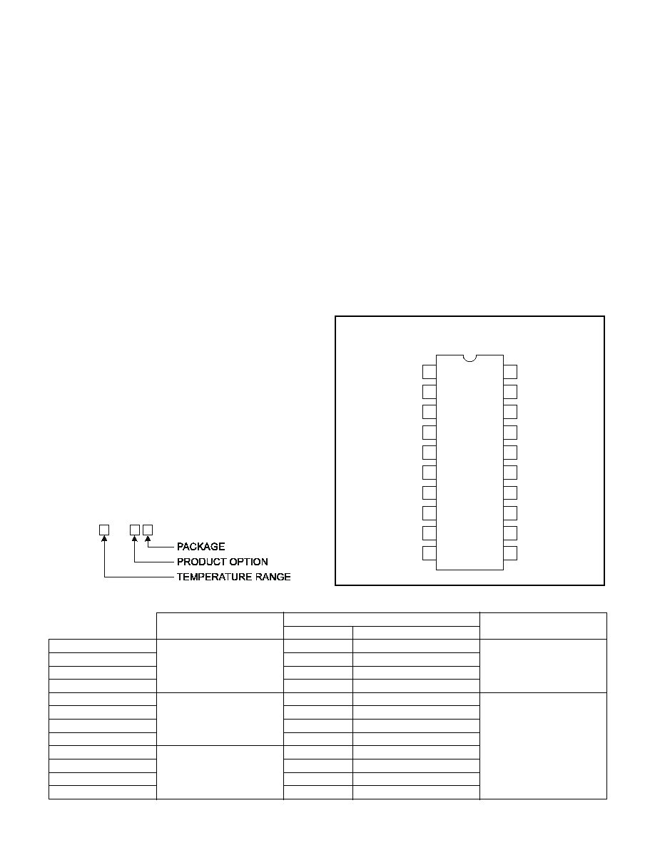
DIL-20, SOIC-20 (TOP VIEW)
N, DW and J Packages
ABSOLUTE MAXIMUM RATINGS
Supply Voltage V
CC
. . . . . . . . . . . . . . . . . . . . . . . . . . . . . . 18V
Gate Drive Current
Continuous . . . . . . . . . . . . . . . . . . . . . . . . . . . . . . . . . . . 0.2A
50% Duty Cycle . . . . . . . . . . . . . . . . . . . . . . . . . . . . . . . . . 1A
Input Voltage
I
SENSE1
, I
SENSE2
MOUT,V
SENSE,
OVP, ENBL, . . . . . . . . 11V
PKLMT . . . . . . . . . . . . . . . . . . . . . . . . . . . . . . . . . . . . . . . 5V
Input Current, R
SET
, I
AC
, PKLMT, ENA . . . . . . . . . . . . . . 10mA
Maximum Negative Voltage, GT1, GT2,
PKLMT, MOUT . . . . . . . . . . . . . . . . . . . . . . . . . . . . . . ≠0.5V
Power Dissipation . . . . . . . . . . . . . . . . . . . . . . . . . . . . . . . . . 1W
Currents are positive into, negative out of the specified termi-
nal. Consult Packaging Section of Databook for thermal limita-
tions and considerations of packages. All voltages are
referenced to GND.
IAC
VFF
VREF
MOUT
ISENSE1
PKLMT
CAOUT
SS2
RT
VAOUT
ISENSE2
GND
VERR
VSENSE
OVP/ENA
CT
GT2
VCC
GT1
20
19
18
17
16
15
14
13
12
11
1
2
3
4
5
6
7
8
9
10
PWRGND
CONNECTION DIAGRAMS
UCC
850
ORDERING INFORMATION
TEMPERATURE RANGE
PRODUCT OPTION
PACKAGE
UVLO
UVLO2 HYSTERESIS
UCC18500
16
1.2
UCC18501
≠55
∞
C to +125
∞
C
10.5
1.2
J-CDIP
UCC18502
16
3.0
N-PDIP
UCC18503
10.5
3.0
DW-SOIC
UCC28500
16
1.2
N-PDIP
DW-SOIC
UCC28501
≠40
∞
C to +85
∞
C
10.5
1.2
UCC28502
16
3.0
UCC28503
10.5
3.0
UCC38500
16
1.2
UCC38501
0
∞
C to +70
∞
C
10.5
1.2
UCC38502
16
3.0
UCC38503
10.5
3.0
PACKAGE INFORMATION
The UCC18500 PFC section incorporates a low offset
voltage amplifier with 7.5V reference, a highly linear mul-
tiplier capable of a wide current range, a high bandwidth,
low offset current amplifier, with a novel noise attenuation
configuration, PWM comparator and latch and a high cur-
rent output driver. Additional PFC features include
over-voltage protection, zero power detection to turn-off
the output when VAOUT is below 0.25V and peak current
and power limiting.
The DC-to-DC section relies on an error signal generated
on secondary-side and processes it by performing peak
current mode control. The DC-to-DC section also fea-
tures current limiting, a controlled soft-start, preset oper-
ating range with selectable options, and 50% maximum
duty cycle.
The UCC38500 and UCC38502 have a wide PFC-UVLO
threshold (16.5V/10V) for bootstrap bias supply opera-
tion. The UCC38501 and UCC38503 are designed with a
narrow UVLO range (10.5V/10V) more suitable for fixed
bias operation. The UCC38500 and UCC38501 have a
narrow UVLO threshold for PWM stage (to allow opera-
tion down to 75% of nominal bulk voltage), while the
UCC38502 and UCC38503 are configured for a much
wider operation range for the PWM stage (down to 50%
of bulk nominal voltage).
DESCRIPTION (cont.)

3
UCC18500/1/2/3
UCC28500/1/2/3
UCC38500/1/2/3
ELECTRICAL CHARACTERISTICS:
Unless otherwise specified, these specifications hold for T
A
=0∞C to 70∞C for the
UCC3850X, ≠40∞C to +85∞C for the UCC2850X, and ≠55∞C to +125∞C for the UCC1850X, T
A
= T
J
. VCC = 12V, RT = 22k, CT =
330pF.
PARAMETER
TEST CONDITIONS
MIN
TYP
MAX
UNITS
Supply Current Section
Supply Current, Off
VCC = 12V (VCC Turn-on Threshold ≠300mV)
150
300
A
Supply Current, On
VCC = 12V
4
6
mA
UVLO Section
VCC Turn-On Threshold (UCCX8500/502)
15.4
16
16.6
V
UVLO Hysteresis (UCCX8500/502)
5.4
6
6.2
V
Shunt Voltage (UCCX8500/502)
I
VCC
= 10mA
17
17.5
V
VCC Turn-On Threshold (UCCX8501/503)
10.2
10.5
10.8
V
UVLO Hysteresis (UCCX8501/503)
0.4
0.5
0.6
V
Voltage Amplifier Section
Input Voltage
T
A
= 0∞C to 70∞C
7.388
7.500
7.613
V
T
A
= ≠40∞C to 85∞C
7.369
7.500
7.631
V
T
A
= ≠55∞C to125∞C
7.313
7.500
7.687
V
V
SENSE
Bias Current
50
nA
Open Loop Gain
VAOUT = 2V to 5V
80
dB
V
OUT
High
I
LOAD
= ≠150 A
5.4
5.5
5.6
V
V
OUT
Low
I
LOAD
= 150
µ
A
0.05
0.10
V
Over Voltage Protection and Enable Section
Over Voltage Reference
7.8
8.0
8.2
V
Hysteresis
400
500
600
mV
Enable Threshold
1
1.5
2
V
Current Amplifier Section
Input Offset Voltage
V
CM
= 0V, V
CAOUT
= 3V
≠5
0
5
mV
Input Bias Current
V
CM
= 0V, V
CAOUT
= 3V
≠50
nA
Input Offset Current
V
CM
= 0V, V
CAOUT
= 3V
25
nA
Open Loop Gain
V
CM
= 0V, V
CAOUT
= 2V to 5V
90
dB
CMRR
V
CM
= 0V to 1.5V, V
CAOUT
= 3V
80
dB
V
OUT
High
I
LOAD
= ≠120 A
6.3
V
V
OUT
Low
I
LOAD
= 1mA
0.2
V
Gain Bandwidth Product
(Note 1)
2.5
MHz
Voltage Reference Section
Input Voltage
TA = 0
∞
C to 70
∞
C
7.388
7.500
7.613
V
TA = ≠40
∞
C to 85
∞
C
7.369
7.500
7.631
V
TA = ≠55
∞
C to 125
∞
C
7.313
7.500
7.687
V
Load Regulation
I
REF
= 1mA to 2mA
5
10
mV
Line Regulation
VCC = 12V to 16V
10
20
mV
Short Circuit Current
VREF = 0V
≠25
mA
Oscillator Section
Initial Accuracy
T
A
= 25∞C
85
100
115
kHz
Voltage Stability
VCC = 10.8V to 15V
1
%
Total Variation
Line, Temp
80
120
kHz
Ramp Peak Voltage
4.5
5
5.5
V
Ramp Amplitude Voltage (peak to peak)
4
V
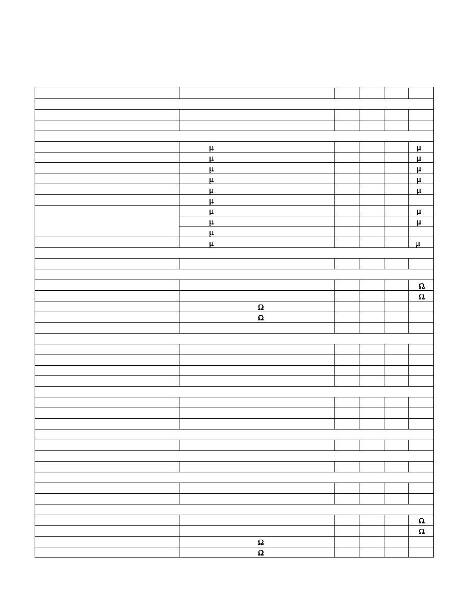
4
UCC18500/1/2/3
UCC28500/1/2/3
ELECTRICAL CHARACTERISTICS:
Unless otherwise specified, these specifications hold for T
A
=0∞C to 70∞C for the
UCC3850X, ≠40∞C to +85∞C for the UCC2850X, and ≠55∞C to +125∞C for the UCC1850X, T
A
= T
J
. VCC = 12V, RT = 22k, CT =
330pF.
PARAMETER
TEST CONDITIONS
MIN
TYP
MAX
UNITS
Peak Current Limit Section
PKLMT Reference Voltage
≠15
0
15
mV
PKLMT Propogation Delay
300
ns
Multiplier Section
High Line, Low Power
I
AC
= 500 A, VFF = 4.7V, VAOUT = 1.25V
≠6
A
High Line, High Power
I
AC
= 500 A, VFF = 4.7V, VAOUT = 5V
≠90
A
Low Line, Low Power
I
AC
= 150 A, VFF = 1.4V, VAOUT = 1.25V
≠19
A
Low Line, High Power
I
AC
= 150 A, VFF = 1.4V, VAOUT = 5V
≠300
A
IAC Limited
I
AC
= 150 A, VFF = 1.3V, VAOUT = 5V
≠300
A
Gain Constant (K)
I
AC
= 300 A, VFF = 2.8V, VAOUT = 2.5V
1
1/V
Zero Current
I
AC
= 150 A, VFF = 1.4V, VAOUT = 0.25V
0
≠2
A
I
AC
= 500 A, VFF = 4.7V, VAOUT = 0.25V
0
≠2
A
I
AC
= 500 A, VFF = 4.7V, VAOUT = 0.5V
≠3
µ
A
Power Limit
I
AC
= 150 A, VFF = 1.4V, VAOUT = 5V
≠420
W
Zero Power Section
Zero Power Comparator Threshold
Measured on VAOUT
0.10
0.25
0.40
V
PFC Gate Driver Section
GT1 Pull Up Resistance
I
OUT
= ≠100mA
7
GT1 Pull Down Resistance
I
OUT
= 100mA
3
GT1 Output Rise Time
C
LOAD
= 1nF, R
LOAD
= 10
25
ns
GT1 Output Fall Time
C
LOAD
= 1nF, R
LOAD
= 10
10
ns
Maximum Duty Cycle
94
%
Second Stage UVLO (UVLO2)
PWM Turn-on Reference (UCCX8500/501)
6.30
6.75
7.30
V
Hysteresis (UCCX8500/501)
1.2
V
PWM Turn-on Reference (UCCX8502/503)
6.30
6.75
7.30
V
Hysteresis (UCCX8502/503)
3
V
Second Stage Soft Start Section
SS2 Charge Current
≠7.5
≠10
≠12.5
µ
A
VERR
I
VERR
= 2mA, UVLO = Low
300
mV
SS2 Discharge Current
ENA = High, UVLO = Low, SS2 = 2.5V
3
10
mA
Second Stage Duty Cycle Clamp Section
Maximum Duty Cycle
44
50
%
Second Stage Pulse by Pulse Current Sense Section
Current Sense Comparator Threshold
VERR = 2.5V, Measured on ISENSE2
.95
1.05
1.15
V
Second Stage Over Current Limit Section
Peak Current Comparator Threshold
1.15
1.30
1.45
V
Input Bias Current
50
nA
Second Stage Gate Driver Section
GT2 Pull Up Resistance
I
OUT
= ≠200mA
7
GT2 Pull Down Resistance
I
OUT
= 100mA
3
GT2 Output Rise Time
C
LOAD
= 1nF, R
LOAD
= 10
25
ns
GT2 Output Fall Time
C
LOAD
= 1nF, R
LOAD
= 10
25
ns
Note 1: Guaranteed by design, not 100% tested in production.

5
UCC18500/1/2/3
UCC28500/1/2/3
UCC38500/1/2/3
CAOUT: (current amplifier output) This is the output of a
wide bandwidth op amp that senses line current and
commands the PFC pulse width modulator (PWM) to
force the correct current. This output can swing close to
GND, allowing the PWM to force zero duty cycle when
necessary.
CT: (Oscillator timing capacitor) A capacitor from CT to
GND will set the oscillator frequency according to:
(
)
f
RT CT
=
∑
0 725
.
GND: (ground) All voltages measured with respect to
ground. VCC and VREF should be bypassed directly to
GND with a 0.1
µ
F or larger ceramic capacitor. The timing
capacitor discharge current also returns to this pin, so
the lead from the oscillator timing capacitor to GND
should be as short and direct as possible.
GT1: (gate drive) The output drive for the PFC stage is a
totem pole MOSFET gate driver on GT1. Use a series
gate resistor of at least 5 ohms to prevent interaction be-
tween the gate impedance and the GT1 output driver that
might cause the GT1 to overshoot excessively. Some
overshoot of the GT1 output is always expected when
driving a capacitive load.
GT2: (gate drive) Same as output GT1 for the second
stage output drive. Limited to 50% maximum duty cycle.
IAC: (input ac current) This input to the analog multiplier
is a current. The multiplier is tailored for very low distor-
tion from this current input (I
AC
) to MOUT, so this is the
only multiplier input which should be used for sensing in-
stantaneous line voltage. Recommended maximum I
AC
is
500
µ
A.
ISENSE1: (current sense) This is the non-inverting input
to the current amplifier. This input and the inverting input
MOUT remain functional down to and below GND.
ISENSE2: (current sense) A resistor from the source of
the lower FET to ground generates the input signal for
the peak limit control of the second stage. The oscillator
ramp can also be summed into this pin, for slope com-
pensation.
MOUT: (multiplier output and current sense amplifier in-
verting input) The output of the analog multiplier and the
inverting input of the current amplifier are connected to-
gether at MOUT. As the multiplier output is a current, this
is a high impedance input so the amplifier can be config-
ured as a differential amplifier to reject ground noise.
Multiplier output current is given by:
(
)
I
VAOUT
I
K V
MO
AC
FF
=
-
∑
∑
1 0
2
.
Connect current loop compensation components be-
tween MOUT and CAOUT.
OVP/ENBL: (over-voltage/enable) A window comparator
input which will disable the PFC output driver if the boost
output is 6.67% above nominal or will disable both the
PFC and second stage output drivers and reset SS2 if
pulled below 1.5V. This input is also used to determine
the active range of the second stage PWM.
PKLMT: (PFC peak current limit) The threshold for peak
limit is 0V. Use a resistor divider from the negative side of
the current sense resistor to VREF to level-shift this sig-
nal to a voltage corresponding to the desired overcurrent
threshold across the current sense resistor.
PWRGND: Ground for totem pole output drivers.
RT: (oscillator charging current) A resistor from RT to
GND is used to program oscillator charging current. A re-
sistor between 10k
and 100k
is recommended.
SS2: (soft start for PWM) SS2 is at ground for either en-
able low or OVP/ENBL below the UVLO2 threshold
conditions. When enabled, SS2 will charge an external
capacitor with a current source. This voltage will be used
as the voltage error signal during start-up, enabling the
PWM duty cycle to increase slowly. In the event of a dis-
able command or a
UVLO2 dropout, SS2 will quickly
discharge to disable the PWM.
VAOUT: (voltage amplifier output) This is the output of
the opamp that regulates output voltage. The voltage am-
plifier output is internally limited to approximately 5.5V to
prevent overshoot.
VCC: (positive supply voltage) Connect to a stable
source of at least 20mA between 12V and 17V for nor-
mal operation. Bypass VCC directly to GND to absorb
supply current spikes required to charge external
MOSFET gate capacitances. To prevent inadequate Gate
Drive signals, the output devices will be inhibited unless
VCC exceeds the upper under-voltage lockout threshold
and remains above the lower threshold.
VERR: Voltage amp error signal for the second stage.
The error signal is generated by an external amplifier
which drives this pin.
VFF: (RMS feed forward signal) VFF signal generated at
this pin by mirroring Iac into a single pole external filter.
PIN DESCRIPTIONS