 | –≠–ª–µ–∫—Ç—Ä–æ–Ω–Ω—ã–π –∫–æ–º–ø–æ–Ω–µ–Ω—Ç: UCC1919 | –°–∫–∞—á–∞—Ç—å:  PDF PDF  ZIP ZIP |
UCC1919
UCC2919
UCC3919
07/99
FEATURES
∑
Precision Fault Threshold
∑
Charge Pump for Low RDS
ON
High Side
Drive
∑
Differential Sense Inputs
∑
Programmable Average Power Limiting
∑
Programmable Linear Current Control
∑
Programmable Fault Time
∑
Fault Output Indicator
∑
Manual and Automatic Reset Modes
∑
Shutdown Control w/Programmable
Softstart
∑
Undervoltage Lockout
∑
Electronic Circuit Breaker Function
3V to 8V Hot Swap Power Manager
10
7
5
6
11
8
9
2
1
12
14
4
GND
CHARGE
PUMP
DRIVER
UVLO
VDD
+
≠
UVLO
+
≠
+
+
≠
200mV
LINEAR
CURRENT
AMPLIFIER
OVERLOAD
COMPARATOR
S
R
Q
Q
RESET
DOMINANT
SET
DOMINANT
+
≠
+
≠
1.5V
0.5V
1.2
µ
A
+
+
1.5v
13
VDD
36
µ
A
50mV
VDD
CSP
CSN
IMAX
IBIAS
PL
CT
FLT
GATE
CAP
LR
SD
UVBIAS
VDD
1X
OVERCURRENT
COMPARATOR
UVBIAS
S
R
Q
Q
S
R
Q
Q
FLT
SD
FLT
SD
1X
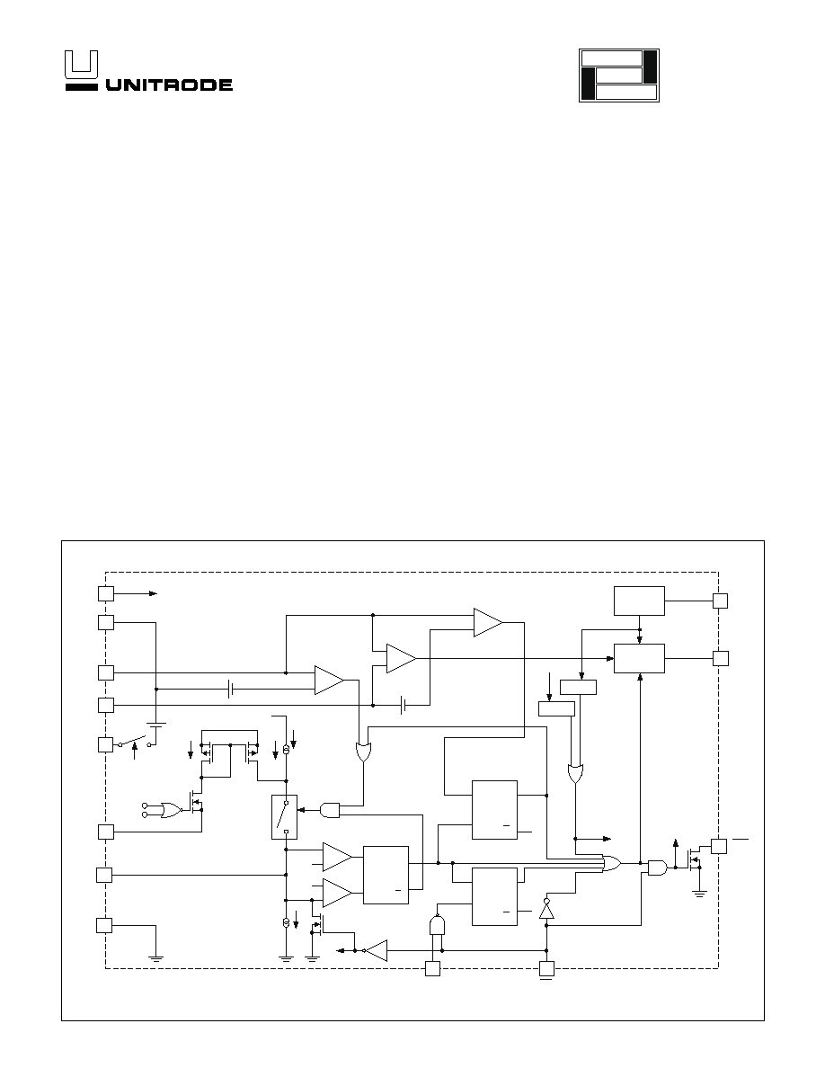
BLOCK DIAGRAM
UDG-98123
DESCRIPTION
The UCC3919 family of Hot Swap Power Managers provide complete
power management, hot swap, and fault handling capability. The
UCC3919 features a duty ratio current limiting technique, which pro-
vides peak load capability while limiting the average power dissipa-
tion of the external pass transistor during fault conditions. The
UCC3919 has two reset modes, selected with the TTL/CMOS com-
patible L/R pin. In one mode, when a fault occurs the IC repeatedly
tries to reset itself at a user defined rate, with user defined maximum
output current and pass transistor power dissipation. In the other
mode the output latches off and stays off until either the L/R pin is re-
set or the shutdown pin is toggled. The on board charge pump circuit
provides the necessary gate voltage for an external N-channel power
FET.
Note: Pins shown for 14-pin package.
application
INFO
available

2
UCC1919
UCC2919
UCC3919
CSN
VDD
CSP
GND
GATE
CT
PL
1
2
3
4
5
6
7
14
13
12
11
10
9
8
IBIAS
IMAX
SD
FLT
N/C
CAP
L/R
CONNECTION DIAGRAMS
ELECTRICAL CHARACTERISTICS:
Unless otherwise specified, VDD = 5V, T
A
= 0∞C to 70∞C for the UCC3919, ≠40∞C
to 85∞C for the UCC2919 and ≠55∞C to 125∞C for the UCC1919. All voltages are with respect to GND. T
A
= T
J
.
PARAMETER
TEST CONDITIONS
MIN
TYP
MAX
UNITS
Input Supply
Supply Current
VDD = 3V
0.5
1
mA
VDD = 8V
1
1.5
mA
Shutdown Current
SD = 0.2V
1
7
µ
A
Undervoltage Lockout
Minimum Voltage to Start
2.35
2.75
3
V
Minimum Voltage after Start
1.9
2.25
2.5
V
Hysteresis
0.25
0.5
0.75
V
IBIAS
Output Voltage, (0 A < I
OUT
< 15 A)
25∞C, referred to CSP
1.47
1.5
1.53
V
Over Temperature Range, referred to CSP
1.44
1.5
1.56
V
Maximum Output Current
1
2
mA
CSN
VDD
CSP
GND
GATE
N/C
PL
CT
1
2
3
4
5
6
7
8
16
15
14
13
12
11
10
9
IBIAS
IMAX
N/C
N/C
CAP
L/R
FLT
SD
DIL-14, (Top View)
N, J Packages
SOIC-16, TSSOP-16 (Top View)
D or PW Package
ABSOLUTE MAXIMUM RATINGS
VDD. . . . . . . . . . . . . . . . . . . . . . . . . . . . . . . . . . . . ≠0.3V to 10V
Pin Voltage
(All pins except CAP and GATE). . . . . . ≠0.3V to VDD + 0.3V
Pin Voltage
(CAP and GATE) . . . . . . . . . . . . . . . . . . . . . . . . ≠0.3V to 15V
PL Current . . . . . . . . . . . . . . . . . . . . . . . . . . . . 0.5mA to ≠10mA
IBIAS Current . . . . . . . . . . . . . . . . . . . . . . . . . . . . . 0mA to 3mA
Storage Temperature . . . . . . . . . . . . . . . . . . . ≠65∞C to +150∞C
Junction Temperature . . . . . . . . . . . . . . . . . . . ≠55∞C to +150∞C
Lead Temperature (Soldering, 10sec.) . . . . . . . . . . . . . +300∞C
Currents are positive into, negative out of the specified termi-
nal. Consult Packaging Section of Databook for thermal limita-
tions and considerations of package.
3
UCC1919
UCC2919
UCC3919
ELECTRICAL CHARACTERISTICS:
Unless otherwise specified, VDD = 5V, T
A
= 0∞C to 70∞C for the UCC3919, ≠40∞C
to 85∞C for the UCC2919 and ≠55∞C to 125∞C for the UCC1919. All voltages are with respect to GND. T
A
= T
J
.
PARAMETER
TEST CONDITIONS
MIN
TYP
MAX
UNITS
Current Sense
Over Current Comparator Offset
Referred to CSP, 3V
VDD
8V
≠55
≠50
≠45
mV
Linear Current Amplifier Offset
V
IMAX
= 100mV, Referred to CSP,
3V
VDD
8V
≠120
≠100
≠80
mV
V
IMAX
= 400mV, Referred to CSP,
3V
VDD
8V
≠440
≠400
≠360
mV
Overload Comparator Offset
V
IMAX
= 100mV, Referred to CSP,
3V
VDD
8V
≠360
≠300
≠240
mV
CSN Input Common Mode Voltage Range
Referred to VDD, 3V
VDD
8V, (Note 1)
≠1.5
0.2
V
CSP Input Common Mode Voltage Range
Referred to VDD, 3V
VDD
8V, (Note 1)
0
0.2
V
Input Bias Current CSN
1
5
µ
A
Input Bias Current CSP
100
200
µ
A
Current Fault Timer
CT Charge Current
V
CT
= 1V
≠56
≠35
≠16
µ
A
CT Discharge Current
V
CT
= 1V
0.5
1.2
1.9
µ
A
On Time Duty Cycle in Fault
I
PL
= 0
1.5
3
6
%
CT Fault Threshold
1.0
1.5
1.7
V
CT Reset Threshold
0.25
0.5
0.75
V
IMAX
Input Bias Current
V
IMAX
= 100mV, Referred to CSP
≠1
0
1
µ
A
Power Limiting Section
Voltage on PL
I
PL
= ≠250
µ
A, Referred to VDD
≠1.0
≠1.4
≠1.9
V
I
PL
= ≠1.5mA, Referred to VDD
≠0.5
≠1.8
≠2.2
V
On Time Duty Cycle in Fault
I
PL
= ≠250
µ
A
0.25
0.5
1
%
I
PL
= ≠1.5mA
0.05
0.1
0.2
%
SD and L/R Inputs
Input Voltage Low
0.8
V
Input Voltage High
2
V
L/R Input Current
1
3
6
µ
A
SD Internal Pulldown Impedance
100
270
500
k
FLT Output
Output Leakage Current
VDD = 5V
10
µ
A
Output Low Voltage
I
OUT
= 10mA
1
V
FET GATE Driver and Charge Pump
Peak Output Current
V
CAP
= +15V, V
GATE
= 10V
≠3
≠1
≠0.25
mA
Peak Sink Current
V
GATE
= 5V
20
mA
Fault Delay
100
300
nS
Maximum Output Voltage
VDD = 3V, Average I
OUT
= 1
µ
A
8
10
12
V
VDD = 8V, Average I
OUT
= 1
µ
A
12
14
16
V
Charge Pump UVLO Minimum Voltage to
Start
VDD = 3V
6.5
7.5
V
VDD = 8V
6.5
8
V
Charge Pump Source Impedance
VDD = 5V, Average I
OUT
= 1
µ
A
50
100
150
k
Note 1: Guaranteed by design. Not 100% tested in production.

4
UCC1919
UCC2919
UCC3919
PIN DESCRIPTIONS
CAP: A capacitor is placed from this pin to ground to fil-
ter the output of the on board charge pump. A .01
µ
F to
0.1
µ
F capacitor is recommended .
CSN: The negative current sense input signal.
CSP: The positive current sense input signal.
CT: Input to the duty cycle timer. A capacitor is con-
nected from this pin to ground, setting the off time and
the maximum on time of the overcurrent protection cir-
cuits.
FLT: Fault indicator. This open drain output will pull low
under any fault condition where the output driver is dis-
abled. This output is disabled when the IC is in low cur-
rent standby mode.
GATE: The output of the linear current amplifier. This pin
drives the gate of an external N-channel MOSFET pass
transistor. The linear current amplifier control loop is in-
ternally compensated, and guaranteed stable for output
load (gate) capacitance between 100pF and .01
µ
F. In
applications where the GATE voltage (or charge pump
voltage) exceeds the maximum Gate-to-Source voltage
ratings (V
GS
) for the external N-channel MOSFET, a
Zener clamp may be added to the gate of the MOSFET.
No additional series resistance is required since the in-
ternal charge pump has a finite output impedance of
100k typical.
GND: The ground reference for the device.
IBIAS: Output of the on board bias generator internally
regulated to 1.5V below CSP. A resistor divider between
this pin and CSP can be used to generate the IMAX volt-
age. The bias circuit is internally compensated, and re-
quires no bypass capacitance. If an external bypass is
required due to a noisy environment, the circuit will be
stable with up to .001
µ
F of capacitance. The bypass
must be to CSP, since the bias voltage is generated with
respect to CSP. Resistor R2 (Figure 4) should be greater
than 50k
to minimize the effect of the finite input imped-
ance of the IBIAS pin on the IMAX threshold.
IMAX: Used to program the maximum allowable sourcing
current. The voltage on this pin is with respect to CSP. If
the voltage across the shunt resistor exceeds this voltage
the linear current amplifier lowers the voltage at GATE to
limit the output current to this level. If the voltage across
the shunt resistor goes more than 200mV beyond this
voltage, the gate drive pin GATE is immediately driven
low and kept low for one full off time interval.
L/R: Latch/Reset. This pin sets the reset mode. If L/R is
low and a fault occurs the device will begin duty ratio cur-
rent limiting. If L/R is high and a fault occurs, GATE will
go low and stay low until L/R is set low. This pin is inter-
nally pulled low by a 3
µ
A nominal pulldown.
PL: Power Limit. This pin is used to control average
power dissipation in the external MOSFET. If a resistor is
connected from this pin to the source of the external
MOSFET, the current in the resistor will be roughly pro-
portional to the voltage across the FET. As the voltage
across the FET increases, this current is added to the
fault timer charge current, reducing the on time duty cy-
cle from its nominal value of 3% and limiting the average
power dissipation in the FET.
SD: Shutdown pin. If this pin is taken low, GATE will go
low, and the IC will go into a low current standby mode
and CT will be discharged. This TTL compatible input
must be driven high to turn on.
VDD: The power connection for the device.
The UCC3919 monitors the voltage drop across a high
side sense resistor and compares it against three differ-
ent voltage thresholds. These are discussed below. Fig-
ure 1 shows the UCC3919 waveforms under fault
conditions.
Fault Threshold
The first threshold is fixed at 50mV. If the current is high
enough such that the voltage on CSN is 50mV below
CSP, the timing capacitor C
T
begins to charge at about
35
µ
A if the PL pin is open. (Power limiting will be dis-
cussed later). If this threshold is exceeded long enough
for C
T
to charge to 1.5V, a fault is declared and the exter-
nal MOSFET will be turned off. It will either be latched off
(until the power to the circuit is cycled, the L/R pin is
taken low, or the SD pin is toggled), or will retry after a
fixed off time (when C
T
has discharged to 0.5V), depend-
ing on whether the L/R pin is set high or low by the user.
The equation for this current threshold is simply:
I
R
FAULT
SENSE
=
0 05
.
(1)
The first time a fault occurs, C
T
is at ground, and must
charge 1.5V. Therefore:
( )
t
t
C
F
FAULT
ON
T
=
=
∑
(sec)
.
µ
1 5
35
(2)
APPLICATION INFORMATION

5
UCC1919
UCC2919
UCC3919
In the retry mode, the timing capacitor will already be
charged to 0.5V at the end of the off time, so all subse-
quent cycles will have a shorter ton time, given by:
( )
t
t
C
F
FAULT
ON
T
=
(sec)
µ
35
(3)
Note that these equations for ton are without the power
limiting feature (R
PL
pin open). The effects of power limit-
ing on ton will be discussed later.
The off time in the retry mode is set by C
T
and an inter-
nal 1.2
µ
A sink current. It is the time it takes C
T
to dis-
charge from 1.5V to 0.5V. The equation for the off time is
therefore:
t
C
F
OFF
T
(sec)
.
=
µ
1 2
(4)
Shutdown Characteristics
When the SD pin is set to TTL high (above 2V) the
UCC3919 is guaranteed to be enabled. When SD is set
to a low TTL (below 0.8V) the UCC3919 is guaranteed to
be disabled, but may not be in ultra low current sleep
mode. When SD is set to 0.2V or less, the UCC3919 is
guaranteed to be disabled and in ultra low current sleep
mode. See Fig. 1.
IMAX Threshold
The second threshold is programmed by the voltage on
IMAX (measured with respect to the CSP pin). This con-
trols the maximum current, I
MAX
, that the UCC3919 will
allow to flow into the load during the MOSFET on time. A
resistive divider connected between IBIAS and CSP gen-
erates the programming voltage. When the drop across
the sense resistor reaches this voltage, a linear amplifier
reduces the voltage on GATE to control the external
MOSFET in a constant current mode.
During this time C
T
is charging, as described above. If
this condition lasts long enough for C
T
to charge to 1.5V,
a fault will be declared and the MOSFET will be turned
off. The I
MAX
current is calculated as follows:
I
V
V
R
MAX
CSP
IMAX
SENSE
=
≠
(5)
Note that if the voltage on the IMAX pin is programmed
to be less than 50mV below CSP, then the UC3919 will
control the MOSFET in a constant current mode all the
time. No fault will be declared and the MOSFET will re-
main on because I
MAX
is less than I
FAULT
.
Overload Threshold
There is a third threshold which, if exceeded, will declare
a fault and shutdown the external MOSFET immediately,
without waiting for CT to charge. This "Overload" thresh-
old is 200mV greater than the IMAX threshold (again,
this is with respect to CSP). This feature protects the cir-
cuit in the event that the external MOSFET is on, with a
load current below I
MAX
, and a short is quickly applied
across the output. This allows hot-swapping in cases
where the UCC3919 is already powered up (on the back-
plane) and capacitors are added across the output bus.
In this case, the load current could rise too quickly for the
linear amplifier to reduce the voltage on GATE and limit
the current to I
MAX
. If the overload threshold is reached,
the MOSFET will be turned off quickly and a fault de-
clared. A latch is set so that C
T
can be charged, guaran-
teeing that the MOSFET will remain off for the same
period as defined above before retrying. The overload
current is:
I
V
V
R
I
R
OVERLOAD
CSP
IMAX
SENSE
MAX
SENSE
=
+
=
+
≠
.
.
0 2
0 2
(6)
Note that I
OVERLOAD
may be much greater than IMAX,
depending on the value of R
SENSE
.
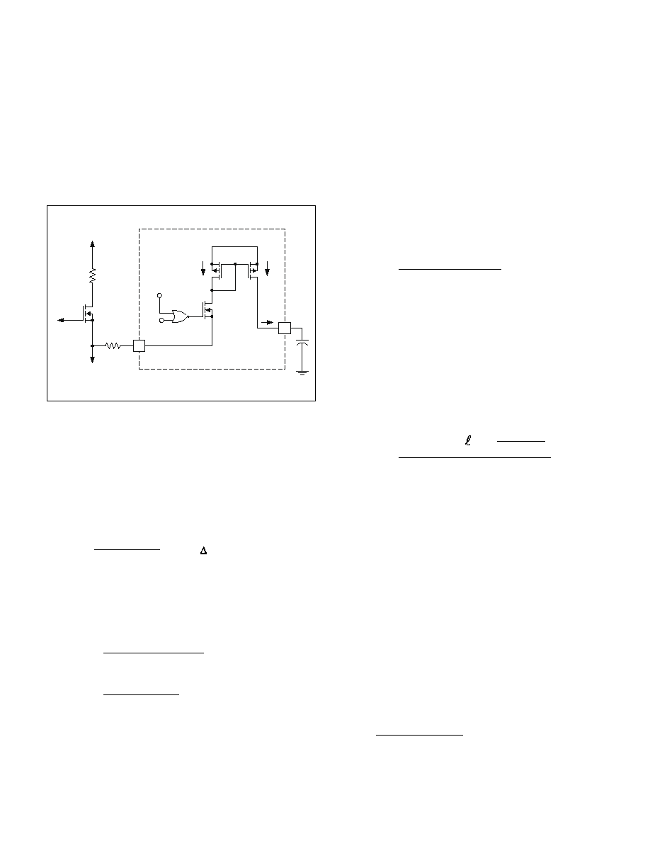
Power Limiting
A power limiting feature is included which allows the
power dissipated in the external MOSFET to be held
relatively constant during a short, for different values of
input voltage. This is accomplished by connecting a re-
sistor from the output (source of the external MOSFET)
to PL. When the output voltage drops due to a short or
overload, an internal bias current is generated which is
equal to:
(
)
I
V
V
V
R
PL
IN
OUT
PL
PL
≠
≠
(7)
APPLICATION INFORMATION
1.e-08
1.e-07
1.e-06
1.e-05
1.e-04
1.e-03
1.e-02
0
0.25
0.5
0.75
1
1.25
1.5
1.75
2
V
SD
I
CC
Figure 1. Typical Shutdown Current
6
UCC1919
UCC2919
UCC3919
This current is used to help charge the timing capacitor
in the event that the load current exceeds I
FAULT
. (A sim-
plified schematic of the circuit internal to the UCC3919 is
shown in Figure 2.) The result is that the on time of the
MOSFET during current limit is reduced as the input volt-
age is increased. This reduces the effective duty cycle,
holding the average power dissipated constant.
It can be seen that power limiting will only occur when I
PL
is > 0 (it cannot be negative). For power limiting to begin
to occur, the voltage drop across the MOSFET must be
greater than VDD-V
PL
or 1.4V(typ).
V
V
V
IN
OUT
-
1 4
.
(8)
The on time using R
PL
is defined as:
t
C
V
I
ON
T
PL
=
∑
+
∑
-
35 10
6
where V = 1V
(9)
The graph in Figure 4 illustrates the effect of R
PL
on the
average MOSFET power dissipation into a short. The
equation for the average power dissipation during a short
is:
P
I
V
I
DISS
MAX
IN
PL
=
∑
∑
∑
+
∑
-
-
1 2 10
35 10
6
6
.
, or
(10)
P
I
V
t
t
t
DISS
MAX
IN
ON
ON
OFF
=
∑
∑
+
If PL is left unconnected, the power limiting feature will
not be exercised. In the retry mode, the duty cycle during
a fault will be nominally 3%, independent of input voltage.
The average power dissipation in the external MOSFET
with a shorted output will be proportional to input voltage,
as shown by the equation:
P
I
V
DISS
MAX
IN
=
∑
∑
0 033
.
(11)
Calculating C
T
(min) for a Given Load Capacitance
without Power Limiting
To guarantee recovery from an overload when operating
in the retry mode, there is a maximum total output ca-
pacitance which can be charged for a given t
ON
(fault
time) before causing a fault. For a worst case situation of
a constant current load below the fault threshold, C
T(min)
for a given output load capacitance (without power limit-
ing) can be calculated from:
C
V
C
I
I
T
IN
OUT
MAX
LOAD
(min)
=
∑
∑
∑
-
-
35 10
6
(12)
A larger load capacitance or a smaller C
T
will cause a
fault when recovering from an overload, causing the cir-
cuit to get stuck in a continuous hiccup mode. To handle
larger capacitive loads, increase the value of C
T.
The
equation can be easily re-written, if desired, to solve for
C
OUT(max)
for a given value of C
T
.
For a resistive load of value RL and an output cap C
OUT
,
C
Tmin
can be smaller than in the constant current case,
and can be estimated from:
C
C
R
n
V
I
R
T
OUT
L
IN
MAX
L
(min)
=
-
∑
∑
-
∑
∑
1
28 10
3
(13)
Note that in the latch mode (or when first turning on in
the retry mode), since the timing capacitor is not recover-
ing from a previous fault, it is charging from 0V rather
than 0.5V. This allows up to 50% more load capacitance
without causing a fault.
Estimating C
T
(min) When Using Power Limiting
If power limiting is used, the calculation of C
T
min for a
given C
OUT
becomes considerably more complex, espe-
cially with a resistive load. This is because the C
T
charge
current becomes a function of V
OUT
, which is changing
with time. The amount of capacitance that can be
charged (without causing a fault) when using power limit-
ing will be significantly reduced for the same value C
T
,
due to the shorter ton time.
The charge current contribution from the power limiting
circuit is defined as:
(
)
I
V
V
V
R
PL
IN
OUT
PL
PL
-
-
(14)
APPLICATION INFORMATION (cont.)
RPL
CT
VDD
UCC3919
POWER LIMIT
1X
1X
TO
GATE
TO
LOAD
VDD
SD
PL
FLT
I
PL
Figure 2. Power limiting circuit.
UGD-98124
7
UCC1919
UCC2919
UCC3919
APPLICATION INFORMATION (cont.)
Figure 3. Typical Timing Diagram
t
0
: Normal condition - Output current is nominal, output
voltage is at positive rail, V
CC
.
t
1
: Fault control reached - Output current rises above
the programmed fault value, C
T
begins to charge with
35
µ
A + I
PL
.
t
2
: Maximum current reached - Output current reaches
the programmed maximum level and becomes a con-
stant current with value I
MAX
.
t
3
: Fault occurs - C
T
has charged to 1.5V, fault output
goes low, the FET turns off allowing no
output current to flow, V
OUT
discharges to GND.
t
4
: Retry - C
T
has discharged to 0.5V, but fault current
is still exceeded, C
T
begins charging again, FET is on,
V
OUT
increases.
t
3
to t
5
: Illustrates <3% duty cycle depending upon
R
PL
selected.
t
6
= t
4
t
7
: Fault released, normal condition - return to normal
operation of the circuit breaker
UDG-97073

8
UCC1919
UCC2919
UCC3919
Constant Current Load
For a constant current load, the output capacitor will
charge linearly. During that time:
(
)
I
avg
V
V
R
V
PL
IN
PL
PL
IN
(
)
-
∑
∑
2
2
(15)
Modifying equation (12) yields:
(
)
C
V
C
V
V
R
V
T
IN
OUT
IN
PL
PL
IN
(min)
∑
∑
-
∑
∑
+
∑
-
2
6
2
35 10
I
I
MAX
LOAD
-
(16)
Resistive Load
Determining C
T
(min) for a resistive load is more complex.
First, the expression for the output voltage as a function
of time is:
V
t
I
R
e
OUT
MAX
LOAD
T
R
C
START
LOAD
OUT
( )
=
∑
-
-
∑
1
(17)
Solving for T
START
when V
OUT
= V
IN
yields:
T
R
C
n
V
I
R
START
LOAD
OUT
IN
MAX
LOAD
=
-
∑
∑
-
∑
1
(18)
Assuming that the device is operating in the retry mode,
where C
T
is charging from 0.5V to just below 1.5V in time
t, C
T
is defined as:
C
I
dt
dV
I
dt
T
CT
CT
=
∑
=
∑
Where
(
)
I
I
CT
PL
=
+
∑
-
35 10
6
(19)
APPLICATION INFORMATION (cont.)
14
13
12
11
0.01
10
9
8
1
CSP
VDD
IMAX
GND
N/C
IBIAS
CSN
PL
R
PL
10k
C
T
0.01
µ
F
C
OUT
R
LOAD
V
OUT
C
IN
2
3
4
5
6
7
0.01
µ
F
CAP
L/R
SD
FLT
R1
4.99k
R2
100k
GATE
CT
V
IN
Figure 5. Application circuit.
UDG-98137
0
0.05
0.1
0.15
0.2
0.25
0.3
1
2
3
4
5
6
VDD (Volts)
PO
WER
D
ISSIP
A
T
ION
(W
atts)
24.9K
20K
15K
10K
R
PL
=
Figure 4. MOSFET average short circuit power
dissipation vs. V
IN
for values of R
PL
.
For I
MAX
=7A

9
UCC1919
UCC2919
UCC3919
Substituting equation (15) into (19) yields:
(
)
C
V
V
R
V
dt
T
IN
PL
PL
IN
(min)
=
-
∑
∑
+
∑
∑
-
2
6
2
35 10
(20)
This yields the following expression for C
T
(min) for a re-
sistive load with power limiting. By substituting the value
calculated for T
START
in equation (18) for dt, C
T
(min) is
determined.
(
)
C
V
V
R
V
T
T
IN
PL
PL
IN
START
(min)
=
∑
∑
∑
+
∑
∑
-
2
6
2
35 10
(21)
Example
The example in Figure 5 shows the UCC3919 in a typical
application. A low value sense resistor and N-channel
MOSFET minimize losses. With the values shown for R1,
R2, and R
S
, the overcurrent fault will be 5A nominal. Lin-
ear current limiting (I
MAX)
will occur at 7.14A and the
overload comparator will trip at 27A. The calculations are
shown below.
I
R
A
FAULT
S
=
=
=
0 05
0 05
0 01
5
.
.
.
(22)
(
)
I
V
V
R
R
R
R
R
A
MAX
CSP
IMAX
S
S
=
-
=
∑
+
∑
=
1 5
1
1
2
714
.
.
(23)
I
I
R
A
A
OVERLOAD
MAX
S
=
+
=
+
=
0 2
714
0 2
0 01
27 14
.
.
.
.
.
(24)
T
C
F
ms
OFF
T
(sec)
.
.
.
.
=
=
=
µ
1 2
0 01
1 2
8 33
(25)
With the value shown for R
PL
:
I
output shorted
V
V
R
PL typ
IN
PL
PL
(
)
(
)
.
=
-
=
-
5 1 6
10
k
A
=
340
µ
(26)
t
shorted
C
I
A
s
ON
T
PL
(
)
.
=
+
∑
=
∑
=
-
-
35 10
0 01 10
375
27
6
6
µ
µ
(27)
P
shorted
I
V
t
t
t
s
DISS
MAX
IN
ON
ON
OFF
(
)
.
=
∑
∑
+
=
∑ ∑
714 5
27
27
µ
µ
s
W
+
∑
=
-
8 33 10
0 12
3
.
.
(28)
For a worst case 1
resistive load: C
OUT
(max)
47
µ
F.
For a worst case 5A constant current load: C
OUT
(max)
27
µ
F.
With L/R grounded, the part will operate in the retry or
"hiccup" mode. The values shown for C
T
and R
PL
will
yield a nominal duty cycle of 0.32% and an off time of
8.3ms. With a shorted output, the average steady state
power dissipation in Q1 will be less than 100mW over the
full input voltage range.
If power limiting is disabled by opening R
PL
, then:
t
t
C
F
s
FAULT
ON
T
=
=
∑
=
sec
µ
µ
1
35
287
(29)
(
)
P
shorted
I
V
t
t
t
DISS
MAX
IN
ON
OFF
ON
=
∑
∑
+
=
∑ ∑
∑
-
714 5
287 10
2
6
.
(
)
87 10
8 33 10
1 2
5
6
3
∑
+
∑
=
=
-
-
.
.
W withV
V
IN
(30)
For a worst case 1
resistive load: C
OUT
(max)
220
µ
F.
For a worst case 5A constant current load: C
OUT
(max)
120
µ
F.
THERMAL CONSIDERATIONS
Steady State Conditions
In normal operation, with a steady state load current be-
low I
FAULT
, the power dissipation in the external MOSFET
will be:
P
RDS
I
DISS
ON
LOAD
=
∑
2
(31)
The junction temperature of the MOSFET can be calcu-
lated from:
(
)
T
T
P
J
A
DISS
JA
=
+
∑
(32)
Where T
A
is the ambient temperature and
JA
is the
MOSFET's thermal resistance from junction to ambient.
If the device is on a heatsink, then the following equation:
JA
JC
CS
SA
+
+
+
(33)
Where
JC
is the MOSFET's thermal resistance from
junction to case,
CS
is the thermal resistance from case
to sink, and
SA
is the thermal resistance of the heatsink
to ambient.
The calculated T
J
must be lower than the MOSFET's
maximum junction temperature rating, therefore:
JA
J
A
DISS
T
T
P
<
-
(max)
(34)
APPLICATION INFORMATION (cont.)

10
UCC1919
UCC2919
UCC3919
Transient Thermal Impedance
During a fault condition in the retry mode, the average
MOSFET power dissipation will generally be quite low
due to the low duty cycle, as defined by:
P
avg
I
V
t
t
t
DISS
MAX
IN
ON
ON
OFF
(
)
=
∑
∑
+
(w/output shorted)
(35)
(In the latch mode, t
OFF
will be the time between a fault
and the time the device is reset.)
However, the pulse power in the MOSFET during t
ON
,
with the output shorted, is:
P
pulse
I
V
DISS
MAX
IN
(
)
=
∑
(w/output shorted)
(36)
In choosing t
ON
for a given V
IN
, I
MAX
, and duty cycle it is
important to consult the manufacturer's transient thermal
impedance curves for the MOSFET to make sure the de-
vice is within its safe operating area. These curves pro-
vide the user with the effective thermal impedance of the
device for a given time duration pulse and duty cycle.
Note that some of the impedance curves are normalized
to one, in which case the transient impedance values
must be multiplied by the DC (steady state) thermal re-
sistance,
JC
.
For duty cycles not shown in the manufacturer's curves,
the transient thermal impedance for any duty cycle and
ton time (given a square pulse) can be estimated from
[1]:
(
)
(
)
JC
JC
SP
trans
D
D
(
)
=
∑
+ -
∑
1
(37)
where D is the duty cycle:
t
t
t
ON
ON
OFF
+
.
and
SP
is the single pulse thermal impedance given in
the transient thermal impedance curves for the time du-
ration of interest (t
ON
). Note that these are absolute num-
bers, not normalized. If the given single pulse impedance
is normalized, it must first be multiplied by
JC
before us-
ing in the equation above.
This effective transient thermal impedance, when multi-
plied by the pulse power, will give the transient tempera-
ture rise of the die. To keep the junction temperature
below the maximum rating, the following must be true:
(
)
(
)
JC
J
C
DISS
trans
T
T
P
pulse
(
)
max
=
-
(38)
If necessary, the junction temperature rise can be re-
duced by reducing ton (using a smaller value for C
T
), or
by reducing the duty cycle using the power limiting fea-
ture already discussed. Note that in either case, the
amount of load capacitance, C
OUT
, that can be charged
before causing a fault, will also be reduced.
Safety Recommendations
Although the UCC3919 is designed to provide system
protection for all fault conditions, all integrated circuits
can ultimately fail short. for this reason, if the UCC3919
is intended for use in safety critical applications where
UL or some other safety rating is required, a redundant
safety device such as a fuse should be placed in series
with the device. The UCC3919 will prevent the fuse from
blowing for virtually all fault conditions, increasing system
reliability and reducing maintenance cost, in addition to
providing the hot swap benefits of the device.
References
[1]
International Rectifier, HEXFET Power MOSFET Design-
er's Manual, Application Note 949B,
Current Ratings, Safe
Operating Area, and High Frequency Switching Perform-
ance of Power HEXFETs, pp.1553-1565, September 1993.
APPLICATION INFORMATION
UNITRODE CORPORATION
7 CONTINENTAL BLVD. ∑ MERRIMACK, NH 03054
TEL. (603) 424-2410 FAX (603) 424-3460

IMPORTANT NOTICE
Texas Instruments and its subsidiaries (TI) reserve the right to make changes to their products or to discontinue
any product or service without notice, and advise customers to obtain the latest version of relevant information
to verify, before placing orders, that information being relied on is current and complete. All products are sold
subject to the terms and conditions of sale supplied at the time of order acknowledgement, including those
pertaining to warranty, patent infringement, and limitation of liability.
TI warrants performance of its semiconductor products to the specifications applicable at the time of sale in
accordance with TI's standard warranty. Testing and other quality control techniques are utilized to the extent
TI deems necessary to support this warranty. Specific testing of all parameters of each device is not necessarily
performed, except those mandated by government requirements.
CERTAIN APPLICATIONS USING SEMICONDUCTOR PRODUCTS MAY INVOLVE POTENTIAL RISKS OF
DEATH, PERSONAL INJURY, OR SEVERE PROPERTY OR ENVIRONMENTAL DAMAGE ("CRITICAL
APPLICATIONS"). TI SEMICONDUCTOR PRODUCTS ARE NOT DESIGNED, AUTHORIZED, OR
WARRANTED TO BE SUITABLE FOR USE IN LIFE-SUPPORT DEVICES OR SYSTEMS OR OTHER
CRITICAL APPLICATIONS. INCLUSION OF TI PRODUCTS IN SUCH APPLICATIONS IS UNDERSTOOD TO
BE FULLY AT THE CUSTOMER'S RISK.
In order to minimize risks associated with the customer's applications, adequate design and operating
safeguards must be provided by the customer to minimize inherent or procedural hazards.
TI assumes no liability for applications assistance or customer product design. TI does not warrant or represent
that any license, either express or implied, is granted under any patent right, copyright, mask work right, or other
intellectual property right of TI covering or relating to any combination, machine, or process in which such
semiconductor products or services might be or are used. TI's publication of information regarding any third
party's products or services does not constitute TI's approval, warranty or endorsement thereof.
Copyright
©
1999, Texas Instruments Incorporated