 | –≠–ª–µ–∫—Ç—Ä–æ–Ω–Ω—ã–π –∫–æ–º–ø–æ–Ω–µ–Ω—Ç: UCC2305N | –°–∫–∞—á–∞—Ç—å:  PDF PDF  ZIP ZIP |
UCC2305
UCC3305
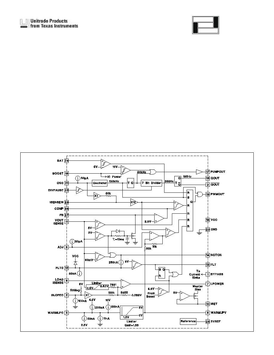
BLOCK DIAGRAM
SLUS297A - SEPTEMBER 1995 - REVISED AUGUST 2001
∑
Regulates Lamp Power
∑
Compensates For Lamp
Temperature
∑
Fixed Frequency Operation
∑
Current Mode Control
∑
Overcurrent Protected
∑
Overvoltage Shutdown
∑
Open and Short Protected
∑
High Current FET Drive Output
∑
Operates Over Wide Battery
Voltage Range: 5V to 18V
The UCC3305 integrates all of the functions required to control and drive one
HID lamp. The UCC3305 is tailored to the demanding, fast turn-on requirements
of automobile headlamps, but is also applicable to all other lighting applications
where HID lamps are selected. HID lamps are ideal for any lighting applications
that can benefit from very high efficiency, blue-white light color, small physical
lamp size, and very long life.
The UCC3305 contains a complete current mode pulse width modulator, a lamp
power regulator, lamp temperature compensation, and total fault protection.
Lamp temperature compensation is critical for automobile headlamps, because
without compensation, light output varies dramatically from a cold lamp to one
that is fully warmed up.
The UCC2305 is tested for full performance with ambient temperature
from ≠40
∞
C to +105
∞
C while the UCC3305 is tested with ambient temperature
from 0
∞
C to +70
∞
C. The UCC3305 is available in a 28 pin small-outline, surface
mount plastic package (SOIC).
HID Lamp Controller
FEATURES
DESCRIPTION
UDG-94091-1
application
INFO
available
2
UCC2305
UCC3305
ABSOLUTE MAXIMUM RATINGS
VCC Supply Voltage. . . . . . . . . . . . . . . . . . . . . . . . . . . . . . 8.0V
BOOST Supply Voltage . . . . . . . . . . . . . . . . . . . . . . . . . . 12.0V
PWMOUT Current, Peak
. . . . . . . . . . . . . . . . . . . . . . . . . . . . ±
1.0A
PWMOUT Energy, Capacitive Load . . . . . . . . . . . . . . . . . 5.0
µ
J
Input Voltage, Any Input. . . . . . . . . . . . . . . . . . ≠0.3V to +10.0V
Output Current, QOUT, QOUT, FLT . . . . . . . . . . . . . .
±
10.0mA
Output Current, 5VREF, LPOWER, COMP . . . . . . . . .
±
10.0mA
ISET Current . . . . . . . . . . . . . . . . . . . . . . . . . . . . . . . . . ≠1.0mA
Storage Temperature . . . . . . . . . . . . . . . . . . .
-
65
∞
C to +150
∞
C
Junction Temperature . . . . . . . . . . . . . . . . . . .
-
55
∞
C to +150
∞
C
Lead Temperature . . . . . . . . . . . . . . . . . . . . . . . . . . . . . +300
∞
C
All voltages with respect to GND. Currents are positive into, neg-
ative out of the specified terminal. Consult Packaging Section of
Databook for thermal limitations and considerations of pack-
ages.
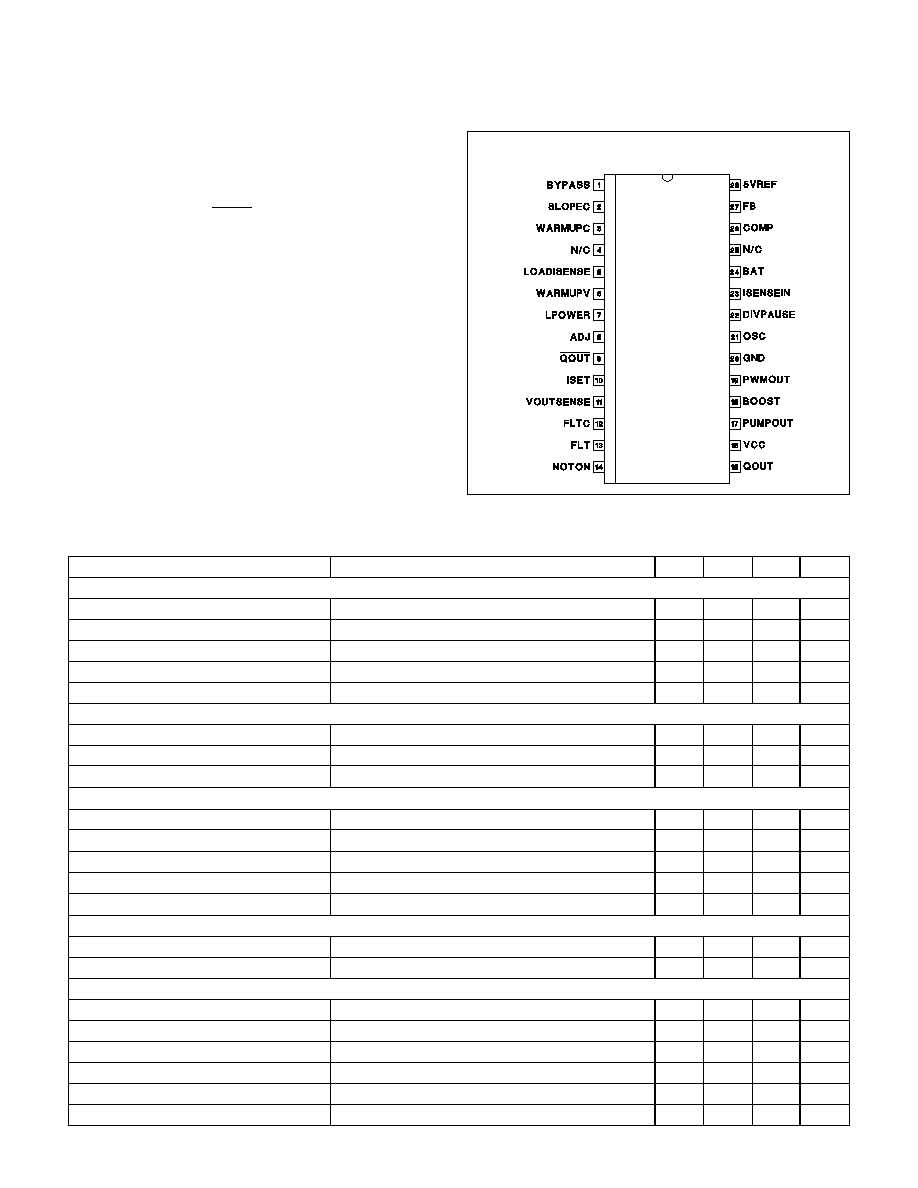
CONNECTION DIAGRAM
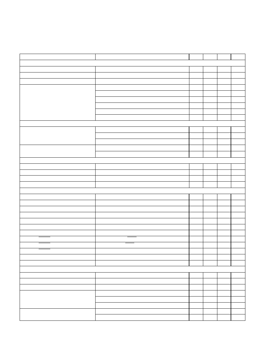
ELECTRICAL CHARACTERISTICS
Unless otherwise stated, VCC = 6.6V, ISET = 100k
to GND, ADJ = 100k
to GND,
OSC = 200pF to GND, BAT = 4V, LOADISENSE connected to LPOWER, VOUTSENSE = 0.666V, BOOST = 10.5V, COMP
connected to FB through a 100k
resistor, ≠40
∞
C<T
A
<+105
∞
C for the UCC2305, 0
∞
C<T
A
<+70
∞
C for the UCC3305, and T
A
=T
J
.
PARAMETER
TEST CONDITIONS
MIN.
TYP.
MAX. UNITS
Overall Section
VCC Supply Current
0.1
1.0
mA
BOOST Supply Current
3.0
5.0
mA
BOOST Threshold to PUMP Stop
9.1
9.6
10.2
V
BOOST Threshold to PUMP Start
9.2
9.7
10.3
V
BOOST Threshold to PWMOUT
4.7
5.4
6.1
V
Battery Section
BAT Threshold to PWMOUT Stop
4.7
5.0
5.3
V
BAT Threshold to PWMOUT Start
4.15
4.8
5.0
V
BAT Input Current
BAT = 4V
≠1
1
µ
A
Oscillator & Divider Section
OSC Frequency
80
100
120
kHz
OSC Pull-Up Current
OSC = 1.5V
-
70
-
50
-
40
µ
A
DIVPAUSE Threshold to Pause
1.1
1.5
1.9
V
DIVPAUSE Threshold to Divide
0.8
1.2
1.6
V
DIVPAUSE Input Current
0V < DIVPAUSE < 6V
≠8
≠5
≠1
µ
A
Reference Section
5VREF Voltage
4.85
5.0
5.1
V
ISET Voltage
4.8
4.8
5.2
V
Error Amplifier Section
FB Voltage
2.4
2.5
2.6
V
FB Input Current
≠1
0
1
µ
A
FB Sink Current
VOUTSENSE = 4V, FB = 4V
0.3
1.5
mA
FB Release Delay
VOUTSENSE Step from 4V to 1V
15
30
43
ms
COMP Source Current
FB = 2V, COMP = 4V
≠3.0
≠0.2
mA
COMP Sink Current
FB = 3V, COMP = 1V
0.2
1.0
mA
PDIP-28 or SOIC-28 (Top View)
N or DW Package
3
UCC2305
UCC3305
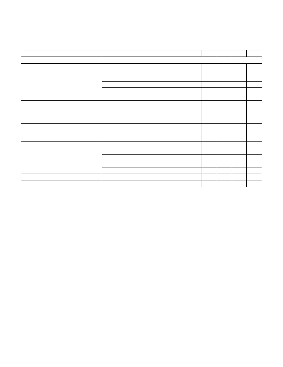
PARAMETER
TEST CONDITIONS
MIN.
TYP.
MAX. UNITS
Load Power Amplifier Section
LOADISENSE Input Current
≠2.5
≠0.1
2.5
µ
A
LPOWER Source Current
LPOWER = 0V
≠8.0
≠0.4
mA
LPOWER Sink Current
LPOWER = 1V
0.4
1.3
mA
LPOWER Voltage
VOUTSENSE = 0.0V
0.32
0.40
0.48
V
VOUTSENSE = 0.45V
0.32
0.40
0.48
V
VOUTSENSE = 0.65V
0.41
0.46
0.51
V
VOUTSENSE = 0.88V
0.43
0.51
0.59
V
VOUTSENSE = 2.0V
0.43
0.51
0.59
V
VOUTSENSE = 0.7V, SLOPEC = 0V
0.29
0.34
0.41
V
Input Current Sense Section
ISENSEIN Threshold
COMP = 5V, WARMUPC = 0V
0.16
0.21
0.28
V
COMP = 5V, WARMUPC = 10V
0.10
0.19
0.27
V
COMP = 1V, WARMUPC = 0V
0.07
0.10
0.2
V
ISENSEIN Bias Current
OSC = 0V
≠15
≠5
≠2
µ
A
OSC = 2V
≠65
≠40
≠15
µ
A
VOUTSENSE Section
VOUTSENSE Threshold to PWMOUT
4.2
5.0
5.2
V
VOUTSENSE Threshold to FB
1.7
1.9
2.1
V
VOUTSENSE Threshold to NOTON
0.035
0.083
0.140
V
VOUTSENSE Input Current
≠1
1
µ
A
OUTPUTS SECTION
PWMOUT High Voltage
I
PWMOUT
= ≠100mA
9.15
10.0
V
PWMOUT Low Voltage
I
PWMOUT
= 100mA
0.3
0.5
V
PUMPOUT High Voltage
I
PUMPOUT
= ≠10mA
5.3
5.8
V
PUMPOUT Low Voltage
I
PUMPOUT
= 10mA
1.0
1.8
V
PUMPOUT Frequency
BOOST = 9.5V
35
50
60
kHz
NOTON High Voltage
I
NOTON
= ≠1mA
5.0
6.3
V
NOTON Low Voltage
I
NOTON
= 1mA
0.1
0.3
V
QOUT, QOUT High Voltage
I
QOUT
= ≠1mA or I
QOUT
= ≠1mA
5.0
6.3
V
QOUT, QOUT Low Voltage
I
QOUT
= 1mA or I
QOUT
= 1mA
0.1
0.45
V
QOUT, QOUT Frequency
150
200
250
Hz
FLT High Voltage
I
FLT
= ≠1mA
6.0
6.3
V
FLT Low Voltage
I
FLT
= 1mA
0.1
0.3
V
Timing Capacitor Section
FLTC Discharge Current
FLTC = 2.5V
35
60
100
nA
FLTC Charge Current
FLTC = 2.5V
≠430
≠300
≠220
nA
FLTC Threshold to FAULT
4.65
4.9
5.1
V
SLOPEC Charge Current
SLOPEC = 0.5V
≠165
≠90
≠60
nA
SLOPEC = 2.2
≠105
≠60
≠40
nA
SLOPEC = 4.2
≠50
≠30
≠10
nA
SLOPEC Voltage
I
SLOPEC
= ≠125nA
1.3
1.5
1.7
V
I
SLOPEC
= ≠50nA
2.8
3.0
3.2
V
ELECTRICAL CHARACTERISTICS (cont.)
Unless otherwise stated, VCC = 6.6V, ISET = 100k
to GND, ADJ = 100k
to GND, OSC = 200pF to GND, BAT = 4V, LOADISENSE connected to LPOWER, VOUTSENSE = 0.666V, BOOST = 10.5V,
COMP connected to FB through a 100k
resistor, ≠40
∞
C<T
A
<+105
∞
C for the UCC2305, 0
∞
C<T
A
<+70
∞
C for the UCC3305, and
T
A
=T
J
.
4
UCC2305
UCC3305
PARAMETER
TEST CONDITIONS
MIN.
TYP.
MAX. UNITS
Timing Capacitor Section (cont.)
SLOPEC Discharge Current
SLOPEC = 2.2V, VCC = 0V, BOOST = 0V,
BYPASS = 8V
40
100
200
nA
WARMUPC Charge Current
WARMUPC = 0V
≠525
≠375
≠275
nA
WARMUPC = 2V
≠525
≠375
≠300
nA
WARMUPC = 6V
≠200
≠120
≠75
nA
WARMUPC Voltage, Charging
I
WARMUPC
= ≠250nA
3.39
3.8
4.1
V
WARMUPC Discharge Current
WARMUPC = 5V, VCC = 0V, BOOST = 0V,
BYPASS = 8V
23
50
126
nA
WARMUPC = 1V, VCC = 0V, BOOST = 0V,
BYPASS = 8V
5
10
30
nA
WARMUPC Voltage, Discharging
I
WARMUPC
= 25nA, VCC = 0V, BOOST = 0V,
BYPASS = 8V
1.5
1.9
2.3
V
ADJ Bias Current
V
ADJ
= 0V
-
38
-
20
-
12
µ
A
WARMUPV Voltage
WARMUPC = 1V
0.05
0.125
0.25
V
WARMUPC = 2V
0.09
1.00
1.5
V
WARMUPC = 3V
2.3
2.48
2.66
V
WARMUPC = 5V
4.5
4.8
5.25
V
WARMUPC = 10V
4.5
4.8
5.25
V
BYPASS Voltage
VCC = 0V
8.8
9.6
V
BYPASS Current
VCC = 0V, BOOST = 0V, BYPASS = 8V
2.5
7
µ
A
ELECTRICAL CHARACTERISTICS (cont.)
Unless otherwise stated, VCC = 6.6V, ISET = 100k
to GND, ADJ = 100k
to GND, OSC = 200pF to GND, BAT = 4V, LOADISENSE connected to LPOWER, VOUTSENSE = 0.666V, BOOST = 10.5V,
COMP connected to FB through a 100k
resistor, ≠40
∞
C<T
A
<+105
∞
C for the UCC2305, 0
∞
C<T
A
<+70
∞
C for the UCC3305, and
T
A
=T
J
.
5VREF: Circuitry in the UCC3305 uses the internal 5V
reference to set currents and thresholds. This reference
can also be used for other functions if required.
ADJ: The ratio of cold lamp peak current to warmed-up
lamp peak current is controlled by the voltage on ADJ. To
select this voltage, connect a resistor from ADJ to GND.
BAT: This input is used to detect excessively high input
voltage and shut down the IC if the input exceeds a pre-
determined level. Connect BAT to a voltage divider
across the input supply. The UCC3305 shuts down when
this input voltage exceeds 5V. To protect the IC in the
event of very high or negative inputs, keep divider imped-
ance higher than 10k.
BOOST: Although the UCC3305 is powered from the
VCC input, most functions of the device operate from a
supply voltage of approximately 10V connected to
BOOST. This 10V supply can be generated by a voltage
doubler using PUMPOUT as an AC signal and external
diodes as switches.
BYPASS: The UCC3305 compensates for lamp tempera-
ture changes by changing the voltage on the SLOPEC
and WARMUPC capacitors. These voltages rise as the
lamp warms up. An internal calculation determines what
power should be applied to the lamp.
When the HID lamp is turned off, power to the lamp and
the controller is removed, leaving these two critical ca-
pacitors charged to specific voltages. Also, with power
off, the lamp will cool down at a controlled rate. It is es-
sential that the two capacitors discharge at a similarly
controlled rate so that if the lamp is restarted before the
lamp is fully cooled, the controller will have an estimate
of new lamp temperature, and can again command the
correct power for the lamp.
Power to control the discharge of these capacitors comes
from energy stored in a large capacitor connected to BY-
PASS. The value of the capacitor required can be esti-
mated assuming a maximum BYPASS current of 5
µ
A, a
discharge time of 60s, and a maximum allowable droop
of 5V by:
C = I
t
V
= 5 A
60s
5V
= 60 F
∑
∑
µ
µ
COMP: Differences between commanded lamp power
and desired lamp power are amplified by an error ampli-
fier. This amplifier senses the difference between the
voltage at FB and 2.5V, and drives COMP with an ampli-
fied error voltage. A capacitor is normally connected from
COMP to FB to compensate the overall feedback loop so
that the system will be stable.
PIN DESCRIPTIONS

5
UCC2305
UCC3305
DIVPAUSE: The QOUT and QOUT outputs can be used
to switch lamp polarity in an AC ballast. It is important to
stop polarity switching when the lamp is being lit, so that
the arc across the electrodes can form in the correct
place. Pulling high on DIVPAUSE stops the internal di-
vider which generates the QOUT and QOUT signals, and
thereby freezes the QOUT and QOUT signals.
To stop the divider when the lamp is being lit and start af-
ter the lamp has lit, connect a resistor from NOTON to
DIVPAUSE and a capacitor from DIVPAUSE to GND.
FLTC: The voltage on VOUTSENSE is proportional to
lamp voltage. If that voltage is too high or too low, the
lamp is either open, shorted, or not yet running. During
normal operation, there is a capacitor connected to
FLTC, and this capacitor is discharged to 0V by a current
source inside the UCC3305.
The UCC3305 monitors the voltage on VOUTSENSE
and compares it to an internal 83mV lower threshold and
a 2V upper threshold. If the voltage is outside this win-
dow, then the IC will pull up on FLTC with a current of ap-
proximately 250nA. If the fault remains long enough to
charge the external FLTC capacitor over 5V, the control-
ler declares a catastrophic fault and shuts the IC down.
The IC will stay shut down until power is removed from
BOOST.
If the fault clears before the FLTC capacitor reaches 5V,
the capacitor discharges down to 0V. This discharge cur-
rent is approximately 50nA, representing a five times lon-
ger discharge rate than charge rate.
FLT: If the voltage on the FLTC pin exceeds 5V, indicat-
ing a severe fault, then a latch in the UCC3305 sets and
PWM drive is halted. In addition, the FLT output goes
high to VCC, indicating a serious system fault.
FB: Differences between commanded lamp power and
desired lamp power are amplified by an error amplifier.
This amplifier senses the difference between the voltage
at FB and 2.5V, and drives COMP with an amplified error
voltage.
GND: Ground for all functions is through this pin.
ISENSEIN: The power regulating algorithm in the
UCC3305 HID Controller computes a function of lamp
current and lamp voltage and commands the appropriate
battery current to keep lamp power constant. This appro-
priate battery current is sensed by a connection from
I-SENSEIN to a current sense resistor. This current
sensed pulse width modulation scheme is often referred
to as current mode control.
In addition to this current regulation, the UCC3305 con-
tains peak input current limiting. This limiting is set to
0.2V across the ISENSEIN resistor during normal opera-
tion and 0.4V during starting. The transition from starting
to normal operation is accomplished by the rise of the
WARMUPC capacitor.
Current mode control has an advantage over voltage
mode control in that a current mode loop is easier to
compensate. Current mode control has a disadvantage
compared to voltage mode control in that the loop can
enter into chaotic oscillations at high duty cycles. These
chaotic oscillations can be prevented using slope com-
pensation. The UCC3305 contains internal slope com-
pensation in the form of a current proportional to OSC
voltage on ISENSEIN. This current combined with an ex-
ternal resistor from ISENSEIN to the current sense resis-
tor creates a voltage drop proportional to OSC voltage,
which gives slope compensation.
ISET: Many functions inside the UCC3305 require pre-
cise currents to give well controlled performance. These
controlled currents are programmed by a resistor from
ISET to GND. A resistor of 100k programs the IC to nor-
mal operating current. Lower resistor values increase the
internal currents. Some of the functions which are influ-
enced by this resistor are WARMUPC charging and dis-
charging, SLOPEC charging and discharging, FLTC
charging and discharging, and error amplifier bandwidth
LOADISENSE: Just as ISENSEIN is normally connected
to a current sense resistor which monitors battery cur-
rent, LOADISENSE is normally connected to a resistor
which monitors lamp current. Lamp current is then regu-
lated by the controller such that the correct lamp power is
supplied at every lamp temperature, in conjunction with
the lamp voltage sensed by VOUTSENSE.
LPOWER: LOADISENSE directly drives one input of an
op amp in the UCC3305. This amplifier amplifies the dif-
ference between the desired load current and the actual
load current, and generates an output signal on
LPOWER which feeds the error amplifier.
NOTON: While the lamp is in a fault condition, such as
excessively high or low lamp voltage, NOTON is pulled
high to VCC, indicating that the arc is not yet correct.
When the voltage on VOUTSENSE is within the 83mV to
2V window, NOTON is pulled low.
OSC: The fixed frequency PWM in the UCC3305 oper-
ates at the frequency programmed by the OSC pin.
Typically, a a 200pF capacitor from OSC to GND pro-
grams the PWM frequency at 100kHz. In addition, this
programs the charge pump at 50kHz and the QOUT and
QOUT signals at 192Hz. The actual oscillator frequency
is a function of both the capacitor from OSC to GND and
the resistor from ISET to GND.
PUMPOUT: Although the UCC3305 is powered from the
VCC input, most functions of the device operate from a
supply voltage of approximately 10V connected to
BOOST. In normal operation, this 10V supply is gener-
PIN DESCRIPTIONS (cont.)

6
UCC2305
UCC3305
ated by a voltage doubler using the PUMPOUT pin as
an AC signal and external diodes as switches.
PUMP-OUT is a square wave which swings from VCC
to GND at half of the OSC frequency.
PWMOUT: The output of the pulse width modulator is a
command signal to a power MOSFET switch. This sig-
nal
appears
on
PWMOUT.
In
normal
systems,
PWM-OUT can be directly connected to the gate of an
N-channel power MOSFET such as the IRF540. If the
lead between the UCC3305 and the MOSFET is longer
than a few cm, a 10 ohm resistor from PWMOUT to
gate may be required to dampen overshoot and under-
shoot.
QOUT: The UCC3305 is immediately configured for DC
HID lamps. To operate with AC HID lamps, it is neces-
sary to add a power H-bridge which will toggle lamp
voltage. A practical switching frequency for this toggle
function is the OSC frequency divided by 512, or 192Hz
for a 100kHz oscillator.
The QOUT pin is a logic output which toggles at the
OSC frequency divided by 512, 180 degrees out of
phase with the QOUT pin.
QOUT: The QOUT pin is a logic output which toggles at
the OSC frequency divided by 512, 180 degrees out of
phase with the QOUT pin.
SLOPEC: To track lamp warm-up and cool down, two
capacitors connected to the UCC3305 charge and dis-
charge. One is connected to SLOPEC. The other is con-
nected to WARMUPC. The capacitor connected to
SLOPEC charges up to 5V with a rate controlled by the
resistor from ISET to GND. With a nominal 100k ISET
resistor the charging current into SLOPEC is equivalent
to the current from a 50Meg resistor to 5V.
When power is removed from VCC, SLOPEC dis-
charges at a constant current, nominally 100nA.
VCC: VCC is the main supply input to the UCC3305.
Many functions in the UCC3305 are powered by VCC,
while others are powered by BOOST. VCC should be
clamped to 6.8V by an external zener diode and kept as
close to 6.8V as practical with a low value resistor to the
input supply.
VOUT-SENSE: The VOUTSENSE input is used to
sense lamp voltage, commonly through a 120:1 voltage
divider. For a normal, running HID lamp, the voltage
across the lamp is between 60V and 110V. It takes
higher than 300V to break down the lamp, and it is de-
sirable to limit the voltage on the starter input to 600V
maximum. A lamp voltage less than 10V is indicative of
a shorted lamp.
The UCC3305 regulates lamp power by commanding
the correct lamp current for a given lamp voltage. In ad-
dition, a comparator in the UCC3305 terminates a PWM
cycle if VOUTSENSE reaches 5V, corresponding to
600V on the lamp. This regulates lamp voltage at 600V
when the lamp is not lit. Comparators in the UCC3305
also compare VOUTSENSE to 83mV corresponding to
10V lamp voltage and 2V, corresponding to a 240V
lamp voltage. When the VOUTSENSE voltage is out-
side this window, the lamp is either not lit, shorted, or
open.
WARMUPC: In addition to the capacitor from SLOPEC
to GND, lamp temperature is estimated by the voltage
on a capacitor from WARMUPC to GND. This capacitor
is charged by a 200nA current source to 4.2V and by a
100nA current source from 4.2V to 10V when the lamp
is on, and discharged by 39nA current sink to 2.5V and
11nA current sink to GND when the lamp is off.
WARMUPV: The voltage on WARMUPC is used to
modulate the signal fed to the error amplifier through
FB. However, the impedance on WARMUPC is too high
to be directly used. The UCC3305 contains a buffer am-
plifier which buffers the voltage on WARMUPC and pro-
cesses it to WARMUPV, making a signal appropriate for
driving FB.
PIN DESCRIPTIONS (cont.)
APPLICATIONS INFORMATION
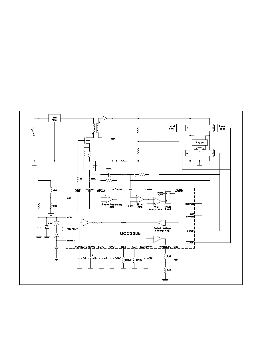
Typical Application
This circuit shows the UCC3305 HID Lamp Controller IC
in a flyback converter. The output of the converter is reg-
ulated at constant power, so that lamp intensity is rela-
tively constant regardless of small lamp manufacturing
variations.
Full Bridge Output Stage
The output of the flyback converter is directed to the AC
lamp through a full bridge inverter. The full bridge is
switched at a low frequency (typically 195Hz), so that the
average lamp voltage is zero. The low frequency switch-
ing is derived from the PWM oscillator. It is desirable to
switch lamp polarity when running, but switching lamp
polarity can interfere with clean starting. The UCC3305
has a logic output called NOTON which is high when the
lamp is not running (Not On) and low when the lamp is
running. This output is connected to the DIVPAUSE input
so that the low frequency switching stops until the lamp
is fully lit.
The UCC3305 HID Controller IC has two low frequency
outputs, QOUT and QOUT. These outputs are capable of
driving low-side MOSFETs directly at 195Hz, but
high-side MOSFETs require a level-shifted drive. This

7
UCC2305
UCC3305
APPLICATIONS INFORMATION (cont.)
can be as simple as a high voltage transistor and a resis-
tor pull-up, combined with the correct choice of phases.
Regulated Lamp Input Power Gives
Constant Intensity
The LPOWER output of the UCC3305 is a voltage
roughly proportional to lamp input power. The UCC3305
regulates constant lamp power over a wide range of lamp
voltages. The range of lamp voltages which produce con-
stant lamp power is set by the limiting amplifier on
VOUTSENSE.
For inputs to VOUTSENSE below 0.5V, such as would
occur with a shorted lamp, the loop regulates constant
load current. For inputs to VOUTSENSE greater than
0.82V, as might occur with a lamp that is open or not yet
lit, the loop also regulates constant load current, but at a
lower current than for a shorted lamp. In between those
two voltages, the amplifier driving the LPOWER pin will
sum the load current and load voltage and produce a sig-
nal roughly proportional to load power. The summing am-
plifier approximates power well enough to hold power
within
±
10% over a factor of two in lamp voltage.
The UCC3305 HID Controller contains a current mode
PWM similar to the industry standard UC3842 and
UCC3802 circuits. This controller uses a high gain op
amp to regulate the output of the LPOWER circuit. This
op amp drives a high speed PWM comparator, which
compares converter input current to the output of the op
amp and uses this signal to set duty cycle.
Slope Compensation
In addition to a complete current mode PWM, the
UCC3305 HID Controller contains internal slope com-
pensation, a valuable function which improves current
loop stability for high duty cycles. Slope compensation is
accomplished with an on-chip current ramp and an
off-chip resistor RSL. Larger values of RSL give more
slope compensation and a more stable feedback loop.
Powering The UCC3305
Conventional power MOSFETs require at least 8V of
gate drive to ensure high efficiency and low on resis-
tance. Despite this requirement, the UCC3305 HID Con-
troller can be used to build a ballast that will drive power
MOSFETs well with input supplies as low as 5V! The
UCC3305 does this using a charge pump.
In this typical application, power for the UCC3305 HID
Controller IC is derived from a 6.8V zener supply. This
zener regulated supply gives the application overvoltage
protection, reverse battery protection, low parts count,
and low cost. The output of the 6.8V zener supply drives
the VCC pin of the UCC3305. VCC is the input to the
UCC3305 charge pump. The charge pump generates a
regulated 10V supply on the BOOST output. This 10V
supply drives all other functions on the UCC3305.
Protection From Over Voltage
The most significant stresses in an automotive environ-
ment are the overvoltage conditions which can occur dur-
ing load dump and double-battery jump start. At these
times, the voltage into the ballast can go so high that
even the most overdesigned power stage will be dam-
aged. The UCC3305 is inherently immune to damage
from this when operated with a zener regulated supply. In
addition, the UCC3305 will protect the ballast compo-
nents by shutting down the PWM in the presence of ex-
cessive voltage on the BAT input.
This typical application shows a voltage divider consist-
ing of a 270k resistor and a 100k resistor driving the BAT
input. The threshold of the BAT input is approximately 5V,
so this divider sets the shutdown voltage at approxi-
mately 18.5V.
Programming the UCC3305
All circuitry on the UCC3305 HID Lamp Controller is op-
erated from a bias current set by the resistor from ISET
to ground. For best operation, this resistor (RSET) should
be between 75k and 150k.
Oscillator Frequency
The UCC3305 HID Lamp Controller PWM oscillator is set
by the resistor from ISET to ground and by the capacitor
from OSC to ground. Oscillator frequency can be esti-
mated by the equation:
FOSC =
2
RSET COSC
∑
For operation at 100kHz, RSET should be 100k and
C
OSC
should be 200pF.
The PWM oscillator also determines the low frequency
lamp switching rate for AC lamps. The exact lamp switch-
ing rate is the PWM frequency divided by 512.
Lamp Temperature Compensation
Automobile headlights must come up to full intensity very
quickly, but HID lamps require many minutes to stabilize.
The UCC3305 HID Controller contains sophisticated in-
ternal circuitry to anticipate lamp temperature and also to
compensate for lamp temperature.
The circuits anticipate lamp temperature by monitoring
charge on capacitors which charge when the lamp is on
and discharge when the lamp is off. The UCC3305 HID
Controller compensates for lamp temperature by driving
the lamp with a higher lamp power when the lamp is cold
and reducing the power to a normal operating level when
the lamp is warmed up. The capacitors which set these
8
UCC2305
UCC3305
time constants are external film capacitors CS and CW,
and are connected to SLOPEC and WARMUPC. CS and
CW are critical capacitors and must be selected to
match the time-temperature relationship of the lamp.
In addition to changing the power regulation point, the
WARMUPC capacitor voltage also changes the short cir-
cuit lamp current. The ratio of cold short circuit current to
warmed-up short circuit current is set by the resistor
from ADJ to ground.
When power is removed from the ballast, CS and CW
must discharge at a controlled rate. The discharge cur-
rents are programmed by current sources on the
UCC3305 HID Controller. These current sources are
powered by the power supply connected to BYPASS. In
a typical application, a non-critical electrolytic capacitor
from BYPASS to ground stores energy when the ballast
is on and uses this energy to control the discharge rate
when the ballast is off.
FLYBACK HID BALLAST
UDG-94092-1
APPLICATIONS INFORMATION (cont.)

IMPORTANT NOTICE
Texas Instruments and its subsidiaries (TI) reserve the right to make changes to their products or to discontinue
any product or service without notice, and advise customers to obtain the latest version of relevant information
to verify, before placing orders, that information being relied on is current and complete. All products are sold
subject to the terms and conditions of sale supplied at the time of order acknowledgment, including those
pertaining to warranty, patent infringement, and limitation of liability.
TI warrants performance of its products to the specifications applicable at the time of sale in accordance with
TI's standard warranty. Testing and other quality control techniques are utilized to the extent TI deems necessary
to support this warranty. Specific testing of all parameters of each device is not necessarily performed, except
those mandated by government requirements.
Customers are responsible for their applications using TI components.
In order to minimize risks associated with the customer's applications, adequate design and operating
safeguards must be provided by the customer to minimize inherent or procedural hazards.
TI assumes no liability for applications assistance or customer product design. TI does not warrant or represent
that any license, either express or implied, is granted under any patent right, copyright, mask work right, or other
intellectual property right of TI covering or relating to any combination, machine, or process in which such
products or services might be or are used. TI's publication of information regarding any third party's products
or services does not constitute TI's approval, license, warranty or endorsement thereof.
Reproduction of information in TI data books or data sheets is permissible only if reproduction is without
alteration and is accompanied by all associated warranties, conditions, limitations and notices. Representation
or reproduction of this information with alteration voids all warranties provided for an associated TI product or
service, is an unfair and deceptive business practice, and TI is not responsible nor liable for any such use.
Resale of TI's products or services with
statements different from or beyond the parameters stated by TI for
that product or service voids all express and any implied warranties for the associated TI product or service,
is an unfair and deceptive business practice, and TI is not responsible nor liable for any such use.
Also see: Standard Terms and Conditions of Sale for Semiconductor Products. www.ti.com/sc/docs/stdterms.htm
Mailing Address:
Texas Instruments
Post Office Box 655303
Dallas, Texas 75265
Copyright
2001, Texas Instruments Incorporated