
UCC2541
SLUS621A - AUGUST 2004 - SEPTEMBER 2005
HIGH EFFICIENCY SYNCHRONOUS BUCK
PWM CONTROLLER
1
www.ti.com
FEATURES
D
On-Chip Predictive Gate Drive
t
for
High-Efficiency Synchronous Buck
Operation
D
Dual
±
3-A TrueDrive
t
Outputs
D
On-Board Programmable Oscillator with
1-MHz Frequency Operation
D
TR Input for Sequencing Operation
D
Overcurrent Protection using a Parallel
Average Current Mode Control Loop
D
3 Modes to Support 2.7-V to 35-V Input Bias
D
Reverse Current Protection for Output Stage
D
User Programmable Shutdown Using SS Pin
D
±
1.0% Initial Tolerance Bandgap Reference
D
High Bandwidth Error Amplifiers
D
Thermally Enhanced HTSSOP 20-Pin
PowerPAD
t
Package and QFN-32 Pin
D
Synchronization Input
D
Supports Pre-Bias Applications
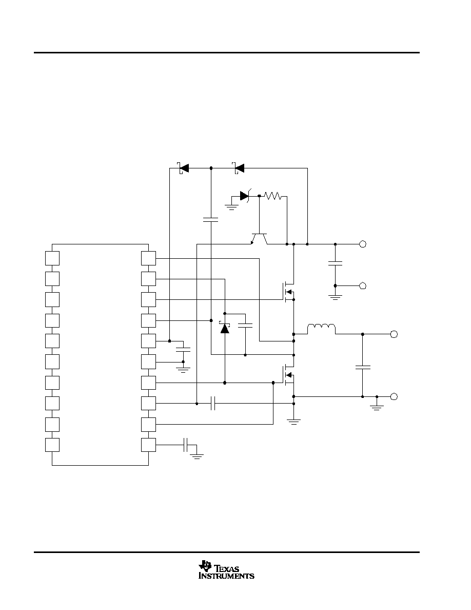
SIMPLIFIED APPLICATION DIAGRAM
APPLICATIONS
D
High Efficiency Non-Isolated Converters
Requiring Advanced Features such as
Pre-Bias Support and Tracking Capability
D
Point-of-Load Modules for Servers, Telecom,
and Data communication Equipments
D
Good for Input Voltages of 3.3 V, 5.0 V,
12.0 V, or Intermediate Bus Voltages
DESCRIPTION
The UCC2541 is a synchronous buck PWM
controller for high current and low output voltage
applications.
For higher efficiency, it incorporates the Predictive
Gate Drive
t
technology that virtually eliminates
body diode conduction losses in synchronous
rectifiers.
VIN
VOUT
RSET
REF
G2C
SYNCIN
GND
RAMP
VEA-
CEA-
SWS
BST
VDD
SW
G1
PGND
G2
VDRV
1
2
3
4
5
6
7
8
20
19
18
17
16
15
14
13
UCC2541
COMP
TR
G2S
SS
9
10
12
11
TR Input
PRODUCTION DATA information is current as of publication date.
Products conform to specifications per the terms of Texas Instruments
standard warranty. Production processing does not necessarily include
testing of all parameters.
Copyright
2004, Texas Instruments Incorporated
Predictive Gate Drive
, TrueDrive
and PowerPAD
are trademarks of Texas Instruments Incorporated.
UCC2541
SLUS621A - AUGUST 2004 - SEPTEMBER 2005
2
www.ti.com
Please be aware that an important notice concerning availability, standard warranty, and use in critical applications of
Texas Instruments semiconductor products and disclaimers thereto appears at the end of this data sheet.
DESCRIPTION (CONT.)
The UCC2541 is available in the extended temperature range of ≠40
∞
C to 105
∞
C and is offered in thermally
enhanced PowerPAD
t
20-pin HTSSOP (PWP) or 32-pin quad flatpack (RHB) package. This space saving
package with standard 20-pin TSSOP footprint has a drastically lower thermal resistance of 1.4
∞
C/W
JC
to
accommodate the dual high-current drivers on board.
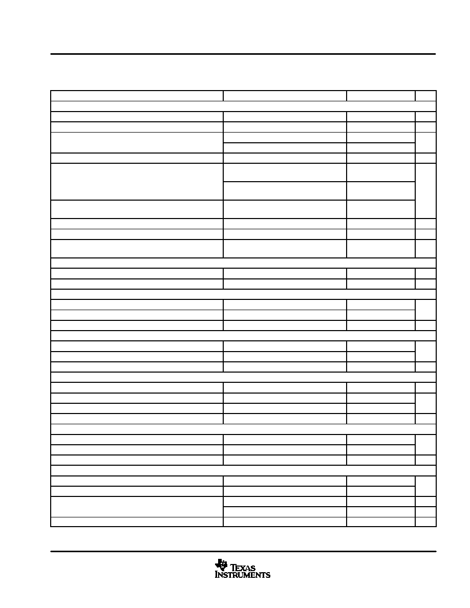
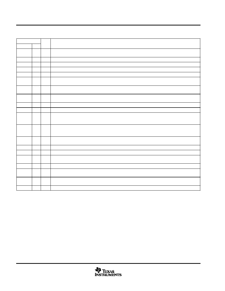
ABSOLUTE MAXIMUM RATINGS
over operating free-air temperature range (unless otherwise noted)
(1)(2)
UCC2541
UNIT
Supply voltage range, VDD
36
V
Supply current, IVDD
VDD
50
mA
CEA-, COMP, G2C, RAMP, SS, TR, VEA-
-0.3 to 3.6
VDRV
-0.3 to 9
Analog input voltages
G1, BST
SW-0.3 to SW+9
V
Analog input voltages
SW, SWS
-1 to 36
V
G2, G2S
-1 to 9
SYNCIN
-0.3 to 8.0
Sink current (peak), IOUT_SINK
G1, G2
3.5
A
Source current (peak), IOUT_SOURCE
G1, G2
-3.5
A
Operating junction temperature range, TJ
-55 to 150
Storage temperature, Tstg
-65 to 150
∞
C
Lead temperature 1,6 mm (1/16 inch) from case for 10 seconds
300
C
(1) Stresses beyond those listed under "absolute maximum ratings" may cause permanent damage to the device. These are stress ratings only,
and functional operation of the device at these or any other conditions beyond those indicated under "recommended operating conditions"
is not implied. Exposure to absolute-maximum-rated conditions for extended periods may affect device reliability.
(2) All voltages are with respect to GND. Currents are positive into, and negative out of the specified terminal.
RECOMMENDED OPERATING CONDITIONS
MIN
TYP
MAX
UNIT
Supply voltage, VDD
Mode 1
8.5
35
Supply voltage, VDRV
Mode 2
4.75
9.00
V
Supply voltage, REF
Mode 3
3.0
3.3
3.6
V
Supply voltage bypass, CVDD
1.0
2.2
Reference bypass capacitor, CREF
0.1
1.0
2.2
F
VDRV bypass capacitor, CVDRV
0.2
µ
F
BST-SW bypass capacitor, CBST-SW
0.1
Timer current resistor range, RRSET
10
50
k
PWM ramp capacitor range, CRAMP
100
680
pF
Turn-off capacitor range, CG2C
120
1000
pF
COMP pin load range, RLOAD
6.5
k
Junction operating temperature, TJ
-40
105
∞
C

UCC2541
SLUS621A - AUGUST 2004 - SEPTEMBER 2005
3
www.ti.com
ORDERING INFORMATION
TA = TJ
HTSSOP-20 (PWP)(1)
QFN-32 (RHB)(1)
TA = TJ
Bulk
Bulk
-40
∞
C to +105
∞
C
UCC2541PWP
UCC2541RHB
(1) The PWP and RHB packages are also available at 73 devices per tube and taped and reeled at
3,000 devices per reel. Add an R suffix to the device type (i.e., UCC2541PWPR). See
the application section of the data sheet for PowerPAD drawing and layout information.
CONNECTION DIAGRAM
1
2
3
4
5
6
7
8
9
10
20
19
18
17
16
15
14
13
12
11
RSET
REF
G2C
SYNCIN
RAMP
GND
VEA-
CEA-
COMP
TR
SWS
BST
G1
SW
VDD
PGND
G2
VDRV
G2S
SS
PWP PACKAGE
(TOP VIEW)
1
2
3
4
5
6
7
8
9
10
11
12
13
14
15
16
24
23
22
21
20
19
18
17
RSET
VREF
G2C
SYNCIN
RAMP
GND
VEA-
CEA-
G1
G1
SW
VDD
PGND
PGND
G2
G2
32
31
30
29
28
27
26
25
NC
NC
NC
NC
NC
SWS
BST
BST
COMP
TR
NC
NC
SS
G2S
NC
VDR
V
RHB PACKAGE
(TOP VIEW)
NC - No internal connection
NOTE: The PowerPAD
t
is not directly connected to any lead of the package, but is thermally connected to the substrate of the device. The
exposed dimension is 1.3 mm x 1.7 mm for the PWP package and 3.25 mm x 3.25 mm for the RHB package. However, the tolerances
can be +1.05 mm / -0.05 mm (+41 mils / -2 mils) due to position and mold flow variation.
THERMAL INFORMATION
PACKAGE
FAMILY
PACKAGE
DESIGNATOR
JA (
∞
C/W)
(with PowerPAD)
JC (
∞
C/W)
(without PowerPAD)
JC (
∞
C/W)
(with PowerPAD)
MAXIMUM DIE
TEMPERATURE
PowerPAD
HTSSOP-20
PWP
22.3 to 32.6
(500 to 0 LFM)
19.9
1.4
125
∞
C
Quad Flatpack
QFN-32
RHB
22.3 to 32.6
(500 to 0 LFM)
19.9
1.4
125
∞
C

UCC2541
SLUS621A - AUGUST 2004 - SEPTEMBER 2005
4
www.ti.com
ELECTRICAL CHARACTERISTICS
VDD = 12 V, 1-
µ
F capacitor from VDD to GND, 1-
µ
F capacitor from BST to SW, 1-
µ
F capacitor from REF to GND, 0.1-
µ
F and 2.2-
µ
F capacitors
from VDRV to PGND, CRAMP = 517 pF, RSET = 10 k
, TA = TJ = -40
∞
C to 105
∞
C, (unless otherwise noted).
PARAMETER
TEST CONDITIONS
MIN
TYP
MAX
UNIT
OVERALL
IVDD
Operating current
DC, after G2 timeout
5
8
10
mA
IVDD
Operating current
CLOAD = 2.2 nF
9
18
30
mA
UNDERVOLTAGE LOCKOUT
VVDD
Start threshold voltage
MODE 1
8.0
8.5
9.0
VVDD
Stop threshold voltage
MODE 1
7.5
8.0
8.5
VVDD
Hysteresis
MODE 1
0.3
0.5
0.8
VVDRV
Start threshold voltage
MODE 2
4.30
4.65
4.85
VVDRV
Stop threshold voltage
MODE 2
4.0
4.3
4.6
V
VVDRV
Hysteresis
MODE 2
0.15
0.35
0.55
V
VREF
Start threshold voltage
MODE 3
VVDD= VVDRV
2.5
2.8
3.2
VREF
Stop threshold voltage
MODE 3
2.2
2.5
2.8
VREF
Hysteresis
MODE 3
0.15
0.35
0.55
VOLTAGE REFERENCE (REF)
VREF
Reference output voltage
TA = 25
∞
C
3.28
3.30
3.35
V
VREF
Reference output voltage
Total variation
3.2
3.3
3.4
V
ISC
Short circuit current
VREF = 0 V,
TA = 25
∞
C
10
13
20
mA
Line regulation
5.25 V
VDRV
7.2 V
0
1.5
15
mV
Load regulation
0 mA
IREF
5 mA
0
30
70
mV
OscillatorPWM (RAMP)
fSW
Oscillator frequency
270
300
330
kHz
DMIN
Minimum duty cycle
0%
VRAMP
Offset voltage
0.10
0.25
0.50
V
Oscillator peak voltage
1.7
2.0
2.3
V
tDEAD
G1 deadtime at maximum duty cycle ratio
150
175
200
ns
IRAMP
Ramp charge current
RRSET = 10 k
-325
-300
-275
µ
A
CURRENT ERROR AMPLIFIER
VCEA+
Offset voltage
Total variation
45
50
55
mV
GBW
Gain bandwidth(3)
3
4
MHz
VOL
Low-level output voltage
ICOMP = 0 A,
VCEA- = 3.3 V,
VVEA- = 2.0 V
0.1
V
VOL
Low-level output voltage
ICOMP = 100
µ
A, VCEA- = 1.5 V
VVEA- = 1 V
0
0.60
0.90
V
VOH
High-level output voltage
ICOMP = 0 A,
VCEA- = 0 V,
VVEA- = 1 V
2.2
2.5
3.0
V
AVOL
Open loop
60
100
160
dB
IBIAS
Bias current
-200
-80
-10
nA
ISINK
Sink current
VCOMP = 1.0 V,
VCEA- = 1.5 V,
VVEA- = 1 V
0.30
0.80
1.70
mA
CMR
Common mode input range(3)
0
2
V
(3) Ensured by design. Not production tested.
UCC2541
SLUS621A - AUGUST 2004 - SEPTEMBER 2005
5
www.ti.com
ELECTRICAL CHARACTERISTICS
VDD = 12 V, 1-
µ
F capacitor from VDD to GND, 1-
µ
F capacitor from BST to SW, 1-
µ
F capacitor from REF to GND, 0.1-
µ
F and 2.2-
µ
F capacitors
from VDRV to PGND, CRAMP = 517 pF, RSET = 10 k
, TA = TJ = -40
∞
C to 105
∞
C, (unless otherwise noted)
PARAMETER
TEST CONDITIONS
MIN
TYP
MAX
UNIT
VOLTAGE ERROR AMPLIFIER
VSS_OFF Offset voltage from soft-start input
VCOMP = VVEA-, VSS- = 1.5 V
0.40
0.75
1.00
V
VTR_OFF Offset voltage from tracking input
VTR = 1.0 V
-10
10
mV
VVEA+
Threshold voltage (from VEA- to COMP)
0
∞
C
TA
105
∞
C
1.485
1.500
1.515
V
VVEA+
Threshold voltage (from VEA- to COMP)
Total variation
1.47
1.50
1.53
V
GBW
Gain bandwidth(3)
3
4
MHz
VOL
Low-level output voltage
ICOMP = 0 A,
VCEA- = 3.3 V,
VVEA- = 2.0 V,
0.1
VOL
Low-level output voltage
ICOMP = 100
µ
A, VCEA- = 0 V,
VVEA- = 1 V,
VTR = 0 V
0
0.60
0.9
V
VOH
High-level output voltage
ICOMP = 0 A,
VCEA- = 0 V
VVEA- = 1 V
2.2
2.5
3.0
AVOL
Open loop
60
100
140
dB
IBIAS
Bias current
-500
-250
-50
nA
ISINK
Sink current
VCOMP = 1.0 V,
VCEA- = 0 V,
VVEA- = 1.0 V,
VTR = 0 V
0.30
0.80
1.70
mA
CURRENT SET
IOUT
Output current
RRSET = 10 k
-158
-150
-142
µ
A
VRSET
RSET voltage
RRSET = 10 k
1.42
1.50
1.58
V
SYNCHRONIZATION AND SHUTDOWN TIMER (SYNCIN, G2C)
Timer threshold
2.3
2.5
2.7
V
SYNCIN threshold
1.50
1.65
1.80
V
ICHG(G2C) Shutdown timer charge current
RRSET = 10 k
-325
-300
-275
µ
A
SOFT-START (SS)
ICH(SS)
Charge current
RRSET = 10 k
-230
-200
-170
A
IDSCH(SS) Discharge current
RRSET = 10 k
45
70
100
µ
A
Discharge/shutdown threshold
0.35
0.45
0.55
V
DRIVE REGULATOR (VDRV)
VVDRV
Output voltage
6.87
7.20
7.53
V
Line regulation
9 V
VVDD
35 V
0
50
100
mV
Load regulation
-5 mA
IVDRV
0 mA
0
50
100
mV
ISC
Short-circuit current
15
30
50
mA
G2S GATE DRIVE SENSE
G2S rising threshold voltage
VSWS = 0 V
1.90
2.25
3.10
V
G2S falling threshold voltage
VSWS = 0 V
1.00
1.25
1.30
V
IG2S
Current
VG2S = 0 V
-0.70
-0.50
-0.37
mA
SWS SWITCH NODE SENSE
SWS rising threshold voltage
VG2S = 0 V
1.90
2.25
2.90
V
SWS falling threshold voltage
VG2S = 0 V
1.0
1.2
1.3
V
ISWS
Current
VSWS = 0 V
-1.8
-1.3
-0.9
mA
ISWS
Current
Outputs disabled
-1.0
1.0
µ
A
Negative threshold voltage
-0.5
-0.3
-0.1
V
(3) Ensured by design. Not production tested.
UCC2541
SLUS621A - AUGUST 2004 - SEPTEMBER 2005
6
www.ti.com
ELECTRICAL CHARACTERISTICS
VDD = 12 V, 1-
µ
F capacitor from VDD to GND, 1-
µ
F capacitor from BST to SW, 1-
µ
F capacitor from REF to GND, 0.1-
µ
F and 2.2-
µ
F capacitors
from VDRV to PGND, CRAMP = 517 pF, RSET = 10 k
, TA = TJ = -40
∞
C to 105
∞
C, (unless otherwise noted)
PARAMETER
TEST CONDITIONS
MIN
TYP
MAX
UNIT
G1 MAIN OUTPUT
RSINK
Sink resistance
VSW = 0 V,
VBST = 6 V,
VG1 = 0.3 V
0.3
0.7
1.3
RSRC
Source resistance
VSW = 0 V,
VBST = 6 V,
VG1 = 5.7 V
10
25
45
ISINK
Sink current(3)
VSW = 0 V,
VBST = 6 V,
VG1 = 3.0 V
3
A
ISRCE
Source current(3)
VSW = 0 V,
VBST = 6 V,
VG1 = 3.0 V
-3
A
tRISE
Rise time
CLOAD = 2.2 nF, from G1 to SW
12
25
ns
tFALL
Fall time
CLOAD = 2.2 nF, from G1 to SW
12
25
ns
G2 SYNCHRONOUS RECTIFIER OUTPUT
RSINK
Sink resistance
VG2 = 0.3 V
5
15
30
ISINK
Sink current(3)
VG2 = 3.25 V
3
A
ISRC
Source current(3)
VG2 = 3.25 V
-3
A
tRISE
Rise time
CLOAD = 2.2 nF, from G2 to PGND
12
25
ns
tFALL
Fall time
CLOAD = 2.2 nF, from G2 to PGND
12
25
ns
VOH
High-level output voltage, G2
VSW = GND
6.2
6.7
7.5
V
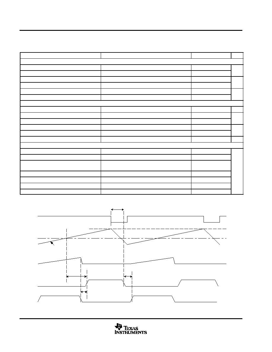
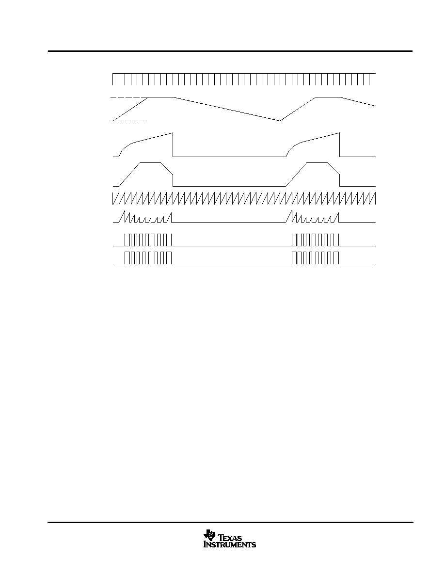
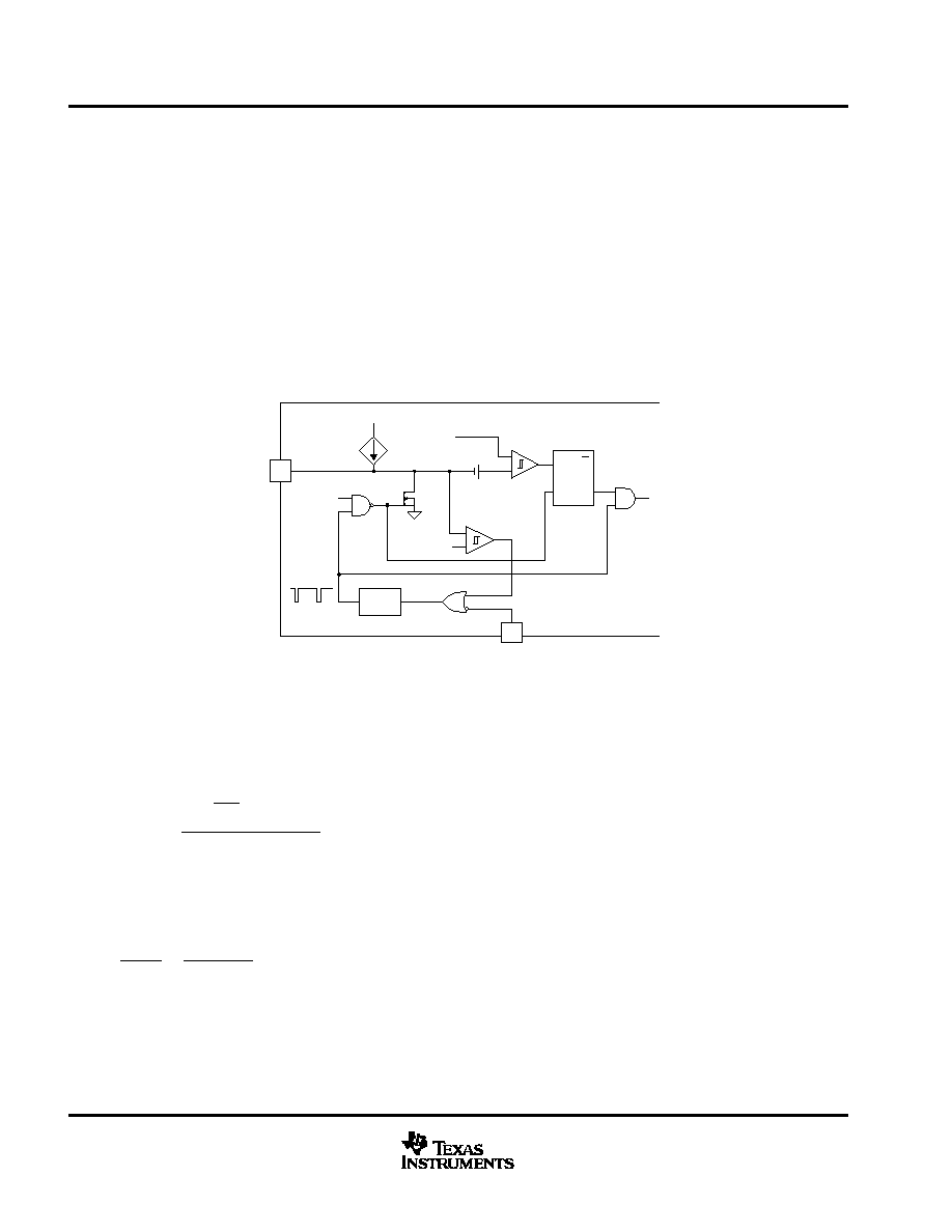
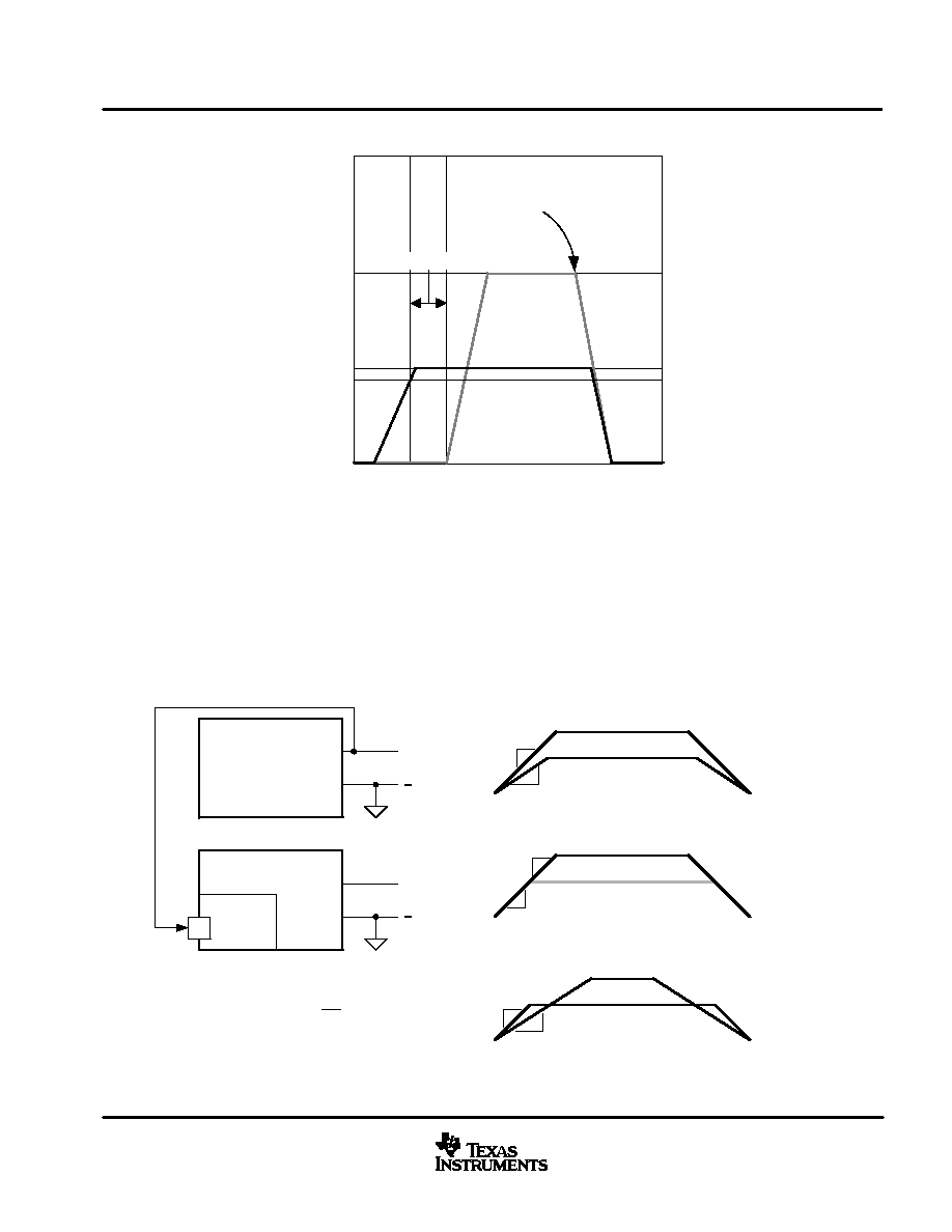
DEADTIME DELAY (see Figure 1)
tON(G1)
RAMP rising to G1 rising
90
115
130
tOFF(G1)
SYNCIN falling to G1 falling
50
70
90
tON(G2)
tOFF(G2)
Delay control resolution
3.5
5.0
6.5
ns
tON(G2)
G2 on-time minimum
wrt G1 falling
-24
ns
tON(G2)
G2 on-time maximum
wrt G1 falling
62
tOFF(G2)
G2 off-time minimum
wrt G1 rising
-68
tOFF(G2)
G2 off-time maximum
wrt G1 rising
10
(3) Ensured by design. Not production tested.
tOFF,G1
t ON,G1
tON,G2
CLK
G1
G2
tOFF,G2
G2C
2.0V
V ERR
RAMP
Figure 1. Predictive Gate Drive Timing Diagram
UCC2541
SLUS621A - AUGUST 2004 - SEPTEMBER 2005
7
www.ti.com
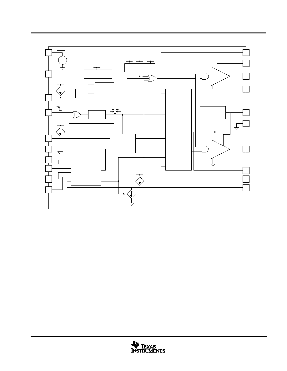
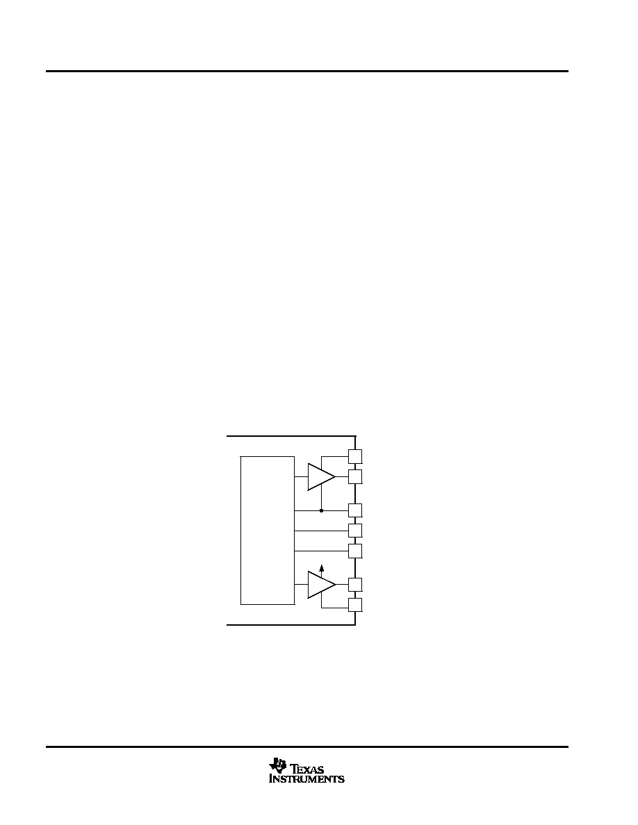
FUNCTIONAL BLOCK DIAGRAM
UVLO
REFERENCE
PREDICTIVE
LOGIC
OSCILLATOR
RAMP
&
PWM LOGIC
CLK
GEN
ERROR
AMPLIFIERS
AND
FAULT LOGIC
1
2
3
4
6
7
8
9
19
16
13
12
11
18
14
10
G2
G1
PGND
VDRV
GND
BST
SW
SYNCIN
RSET
REF
G2C
COMP
VEA-
TR
CEA-
G2S
UVLO
PWM
HUP
VERR
RAMP
CLK
ISET
17
SWS
5
RAMP
15
VDD
DRIVE
REGULATOR
VREF
VREF
SS
LOW SIDE
DRIVER
VDD
VDRV
VREF
PGND
20
PGND
HIGH SIDE
DRIVER
VREF
VREF
PWR
BIAS
PWR
G2 TIMER
G2
GLO
GLO
2 I SET
+
-
1.5V
2 I SET
1.33 I
SET
1.73 I
SET
100ns
G1D
UVLO
G2TO
G1D
VDRV
UCC2541
SLUS621A - AUGUST 2004 - SEPTEMBER 2005
8
www.ti.com
PIN ASSIGNMENTS
TERMINAL
I/O
DESCRIPTION
NAME
NO.
I/O
DESCRIPTION
BST
19
I
Floating G1 driver supply pin. VHI is fed by an external Schottky diode during the SR MOSFET on time. Bypass
BST to SW with an external capacitor.
CEA-
8
I
Inverting input of the current error amplifier used for output current regulation.
COMP
9
I
Output of the voltage and current error amplifiers for compensation.
G1
18
O
High-side gate driver output that swings between SW and BST.
G2
14
O
Low-side gate driver output that swings between PGND and VDRV.
G2C
3
I
Timer pin to turn off synchronous rectifier. The capacitor connected to this pin programs the maximum duration
that G2 is allowed to stay HIGH.
G2S
12
I
Used by the predictive deadtime controller for sensing the SR MOSFET gate voltage to set the appropriate dead-
time.
GND
6
-
Ground for internal circuitry. GND and PGND should be tied together under the device. See layout guidelines for
further details.
PGND
15
-
Ground return for the G2 driver. Connect PGND to the pc-board ground plane with several vias.
RAMP
5
I
Input pin to connect timing capacitor to GND to generate the oscillator PWM ramp.
REF(1)
2
I/O
3.3-V reference pin. All analog control circuits are powered from this 3.3-V rail. Bypass this pin with at least 0.1
µ
F of capacitance for REF loads that are 0 mA to -1 mA. Bypass this pin with at least 1
µ
F of capacitance if it is
used as an input (Mode 3) or if it has large or pulsating loads.
RSET
1
I
Pin to program timer currents for G2C, RAMP, SS charge and SS discharge. This pin generates a current propor-
tional to the value of the external resistor connected from RSET pin to GND. RSET range is 10 k
to 50 k
(giv-
ing a programmable nominal ISET range of 30
µ
A to 150
µ
A, respectively).
SS
11
I
Soft start and shutdown pin. Connect a capacitor to GND to set the soft-start time. Add switch to GND for imme-
diate shutdown functionality.
SYNCIN
4
I
Input pin for timing signal. Tie to logic high (VREF) when not used.
SW
17
-
G1 driver return connection.
SWS
20
I
Used by the predictive controller to sense SR body-diode conduction. Connect to SR MOSFET drain close to the
MOSFET package.
TR
10
I
Tracking input to the voltage error amplifier. Connect to REF when not used.
VDD
16
I
Power supply pin to the device and input to the internal VDRV drive regulator. Normal VDD range is from 4.5 V to
36 V. Bypass the pin with at least 1
µ
F of capacitance.
VDRV
13
I
Output of the drive regulator and power supply pin for the G2 driver. VDRV is also the supply voltage for the in-
ternal logic and control circuitry.
VEA-
7
I
Inverting input of the voltage error amplifier used for output voltage regulation.
(1) REF is an input in Mode 3 only.
UCC2541
SLUS621A - AUGUST 2004 - SEPTEMBER 2005
9
www.ti.com
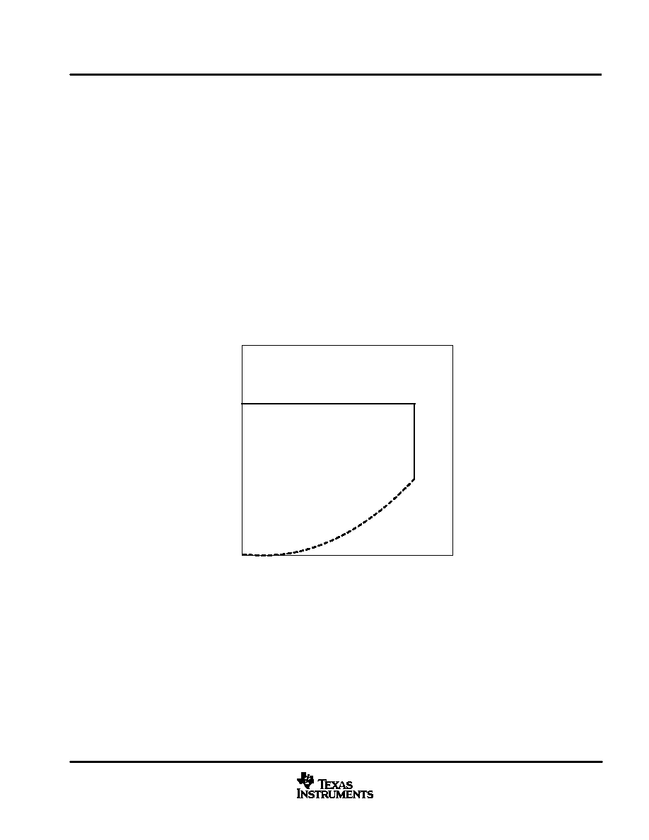
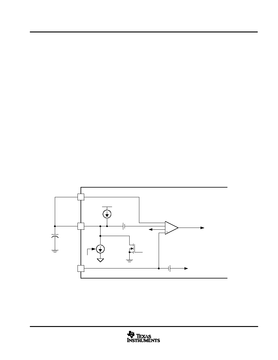
APPLICATION INFORMATION
The UCC2541 is a high-efficiency synchronous buck controller that can be used in many point-of-load
applications.
CEA- and VEA- pins: Current Limit and Hiccup Mode
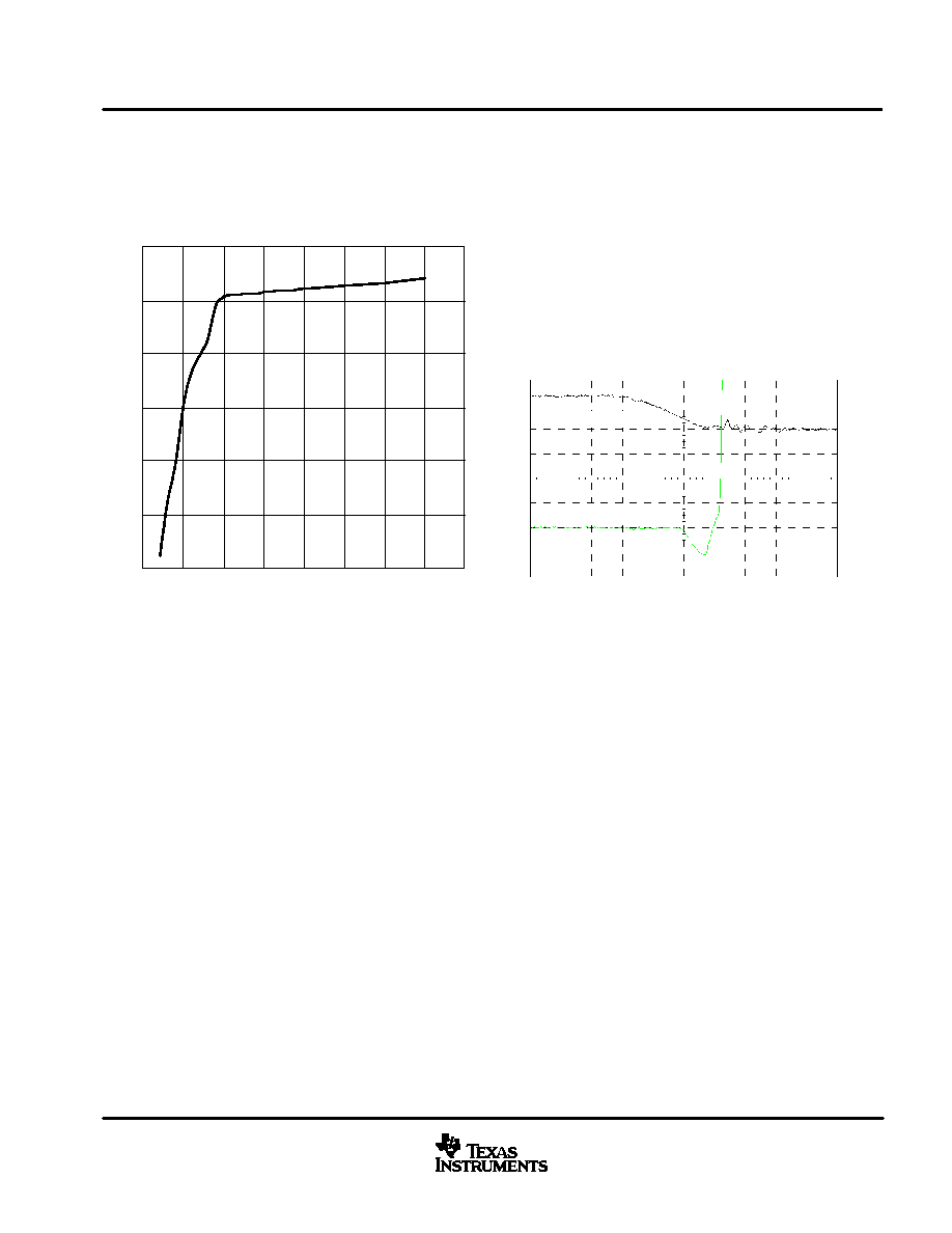
Typical power supply load voltage versus load current is shown in Figure 2. This figure shows steady state
operation for no-load to overcurrent shutdown (soft-start retry is not depicted in the diagram). During the voltage
regulation conditions, the voltage error amplifier output is lower than the current error amplifier, allowing the
voltage error amplifier to control operation. During the current limit conditions, the current error amplifier output
is lower than the voltage error amplifier, allowing the current error amplifier to control operation. The boundary
between voltage and current control occurs when the difference between CEA- and VEA- tries to exceed
50 mV.
Current limiting begins to occur when the difference between CEA- and VEA- exceeds 50 mV. For currents
that exceed this operating condition, the UCC2541 controls the converter to operate as a pure current source
until the output voltage falls to half of its rated steady state level. Then the UCC2541 sets both G1 and G2 outputs
to LOW and it latches a fault that discharges the soft-start voltage at 30% of its charging rate. The UCC2541
inhibits a retry until the soft-start voltage falls below 0.5 V. A functional diagram of the voltage and current error
amplifiers is shown in Figure 3.
UDG-04053
Shutdown
Limited
Current
ILOAD - Load Current - A
V
LOAD
- Load V
o
ltage - V
VREG
Figure 2. Typical Power Supply Load Voltage vs Current

UCC2541
SLUS621A - AUGUST 2004 - SEPTEMBER 2005
10
www.ti.com
APPLICATION INFORMATION
RLOAD
RS
RI1
RV1
RI2
RV2
RFI
CFI
RFV
CFV
ZFV
ZIV
CFIR
VERR to
1.5 V
VEA-
7
8
9
CEA-
UCC2541
+
+
+
Voltage
Error
Amplifier
COMP
Modulator
Current
Error
Amplifier
C
+
+
SS
TR
R
+
1.5 R
50 mV
ZFV
ZIV
From Power MOSFET
Switch Node
1.5 V
Inverting
Amplifier
+
0.7 V
CST
Figure 3. Error Amplifier Configuration
Component selection includes setting the voltage regulation threshold, then the current limit threshold, as
described below.
Voltage vs. Current Programming (refer to Figure 3):
1.
Determine the ratio
R
V1
R
V2
+
V
LOAD(reg)
V
VEA
*
)
Threshold Voltage
*
1 V
+
V
LOAD(reg)
1.5 V (typ)
*
1 V
2.
Sense resistor R
S
+
1
)
R
V1
R
V2
V
CEA
)
offset voltage
I
S(max)
, where I
S(max)
is the current limit level,
V
CEA+
offset = 50 mV (typ).
3.
Arbitrarily select either R
V1
or R
V2
so that the smallest of the two resistors is between 6.5 k
and 20 k
.
Then calculate the value of the other resistor using the equation in the first step.
If the converter is in a current-limit condition and the output voltage falls below half of the regulated output
voltage, the UCC2541 enters into a hiccup (restart-retry) mode. Figure 4 shows typical signals during hiccup
mode.
UCC2541
SLUS621A - AUGUST 2004 - SEPTEMBER 2005
11
www.ti.com
APPLICATION INFORMATION
SYNCIN
SS
RAMP
G2C
G1
G2
0.5 V
3.3 V
ILOAD
VLOAD
UDG-04046
Figure 4. Typical Hiccup Mode waveforms
COMP, VEA- and CEA- pins: Voltage and Current Error Amplifiers
From no-load to full rated load operating conditions, the UCC2541 operates as a voltage mode controller. Above
the programmed rated current, there are two levels of over current protection; constant current limit and
overcurrent reset/retry. This section gives suggestions on how to design the voltage controller and current
controller so that they interact with one another in a stable fashion. Refer to the functional diagram of the voltage
and current error amplifiers in Figure 3. The voltage error amplifier in the figure shows three non-inverting inputs.
The lowest of the three non-inverting inputs (1.5 V, SS and TR) is summed with the inverting input to achieve
the voltage error signal. The lowest of the two outputs drives the inverting stage which in turn, drives the
modulator.
During steady state voltage control operation, the feedback elements in the current loop have no effect on the
loop stability. When current limit occurs, the voltage error amplifier effectively shuts OFF and the current error
amplifier takes control. During steady state current limit operation, the negative feedback elements in the
voltage error amplifier loop become positive feedback elements in the current error amplifier loop. In order for
the current error amplifier to be stable, the impedances in the feedback path of the current error amplifier must
be lower than the impedances in the feedback path of the voltage error amplifier. This means that resistors in
the current error amplifier negative feedback path must be less than the resistors in the voltage error amplifier
negative feedback path. Also capacitors in the current error amplifier negative feedback path must be larger
than capacitors in the negative feedback path of the voltage error amplifier negative feedback path.
(Capacitance is really an admittance value rather than an impedance value). This concept is illustrated in
Figure 3.
In order for the current loop to be stable in Figure 3, ||Z
IV
|| must be less than ||Z
FV
|| over all frequencies. This
can be achieved if R
FI
< R
FV
and C
FI
> C
FV
.

UCC2541
SLUS621A - AUGUST 2004 - SEPTEMBER 2005
12
www.ti.com
APPLICATION INFORMATION
Another issue that can occur during current limit operation is modulator stability. In order for the modulator to
be stable, the rising slope of the current ripple measured at the COMP pin must be smaller than the rising slope
that is measured at the RAMP pin. This can be met either in the selection of the ratio of ||Z
IV
|| to ||Z
FV
||, or by
the addition of a capacitor in parallel to R
FI
and C
FI
, such as C
FIR
, in Figure 3.
In some applications, this current and voltage error amplifier configuration may lead to difficulties with startup
at turn on and with restarting after current limit hiccup operation. A small capacitor from CEA- to ground can
filter this node to alleviate this issue. This capacitor is shown as C
ST
in Figure 3.
Stable Dynamic Current Loop Design (refer to Figure 3):
1.
Using any favorite approach, design the voltage error amplifier for stable voltage mode design. Use at least
15 k
for any resistors in the negative feedback path of the voltage error amplifier (between pins 9 and 7).
This does not apply to resistance values between the power supply output voltage and pin 7; it also does
not apply to resistance values between ground and pin 7.
2.
The goal is to design the current limit control loop so that it drives the converter to maintain 50 mV between
the VEA- pin and the CEA- pin during current-limit conditions. Select the current sense element and the
voltage divider ratios for the VEA- pin to ground and the CEA- pin to ground to provide the desired current
limit level.
3.
Place the same configuration of components in the negative feedback path of the current error amplifier
(between pins 9 and 8), that are in the negative feedback path of the voltage error amplifier (between pins
9 and 7). However, use resistors with values that are 67% of the corresponding resistors that are between
pins 9 and 7 and use capacitors that are 150% of the corresponding capacitors that are between pin 9 and
pin 7.
4.
Check the COMP signal. If it is unstable, place a capacitor (or increase the capacitance) between pins 9
and 8 in order to attenuate the current ripple. Raise the value of the capacitor until the COMP pin voltage
becomes stable. Compare the COMP voltage with the RAMP voltage. With stable operation, the rising slope
of the COMP voltage ripple is less than the rising slope of the RAMP pin.
UCC2541
SLUS621A - AUGUST 2004 - SEPTEMBER 2005
13
www.ti.com
APPLICATION INFORMATION
RSET, RAMP, G2C, SS pins: Programming the Timer Currents
Set the base current to the timers with a resistor between RSET and GND. The block diagram of the UCC2541
shows the interaction of the RSET pin and the dependent current sources for the RAMP, G2C and SS features.
The RSET pin is a voltage source; the current of the RSET pin is reflected and multiplied by a gain and distributed
to the RAMP (gain = 2), G2C (gain = 2) and SS (charge gain = 1.33, net discharge gain = 0.4). The resistance
applied to the RSET pin and GND should be in the range of 10 k
< R
RSET
< 50 k
. RAMP, G2C and SS timers
are programmed by the selection of capacitors tied between each of their respective pins and GND.
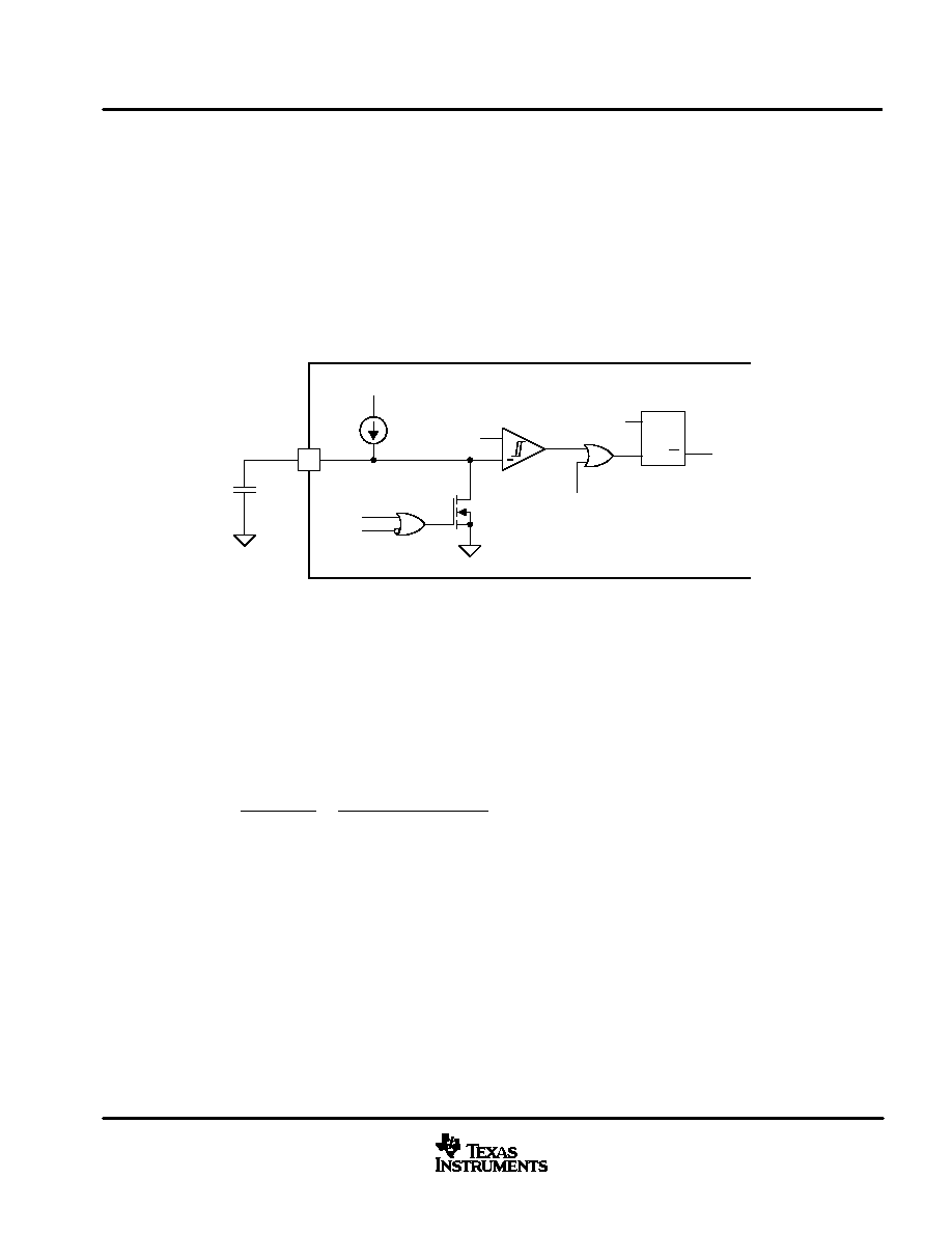
G2C pin: G2 Timer for Output Stage Reverse Current Protection
3
G2C
+
S
Q
Q
G2C
Latch
G2TO
G2 Timeout
Comparator
2.5 V
UVLO
*G1D
GLO
G2
*G1 with delay, but not blanked
UDG-04047
CG2C
2
y
IRSET
RD
Figure 5. Functional diagram of the G2 Timer
The G2C pin programs the maximum duration of the synchronous rectifier to facilitate low or zero duty ratio
operation. Figure 5 shows the functional diagram. This function is programmed by connecting a capacitor
between the G2C pin and GND. The capacitor on G2C should be slightly larger than the capacitor on the RAMP
pin. For best results, program the typical G2 time limit to be between 1.5 and 3 times the switching period (T).
Notice that when the G2 timer reaches its limit, both G1 and G2 are forced to a LOW output. This feature
prevents the current in the output inductor from excessive negative excursions during zero-duty ratio conditions.
Program the G2 time-out (G2TO) duration using equation (1):
C
G2C
+
2
V
RSET
R
RSET
G2 Timeout Duration
G2C Timer Threshold
, Farads
where
D
V
RSET
= 1.5 V(typ)
D
1.5 T < G2 Timeout Duration < 3T
S
D
G2C Timer Threshold = 2.5 V (typ)
(1)
UCC2541
SLUS621A - AUGUST 2004 - SEPTEMBER 2005
14
www.ti.com
APPLICATION INFORMATION
RAMP pin: Oscillator and PWM Ramp
The RAMP pin serves two purposes: (1) a capacitor on this pin sets the oscillator charging time to program the
frequency of operation for the converter and (2) the peak voltage on RAMP defines the gain of the PWM
modulator. The UCC2541 has a leading edge modulator that compares the error output with the RAMP voltage.
A diagram of the oscillator and PWM modulator is shown in Figure 6.
The current charging the capacitor from RAMP to ground is equal to 2 x I
RSET
. In the UCC2541, with leading
edge modulation, a switching cycle can be considered to begin when the oscillator ramp reaches 2.0 V. This
voltage level triggers the negative-going clock signal which enables the RAMP discharge transistor and
simultaneously sends a G1 turn-off command to the PWM control. The internal clock signal is held low for
approximately 100 ns, and this sets the maximum desired value for the capacitor on the RAMP pin. Note that
the RAMP discharge transistor must also sink 2 x I
RSET
while it is discharging the external RAMP capacitor.
2
y
IRSET
VERR
5
S
RD
Q
Q
+
-
+
0.25V
2.0 V
CLK
ENA
RAMP
PWM
PWM
LATCH
PWM
COMPARATOR
OSC RAMP
COMPARATOR
CLK
GEN
4
SYNCIN
+
-
Figure 6. Oscillator and PWM Modulator
The oscillator frequency is programmed by proper selection of the resistor connected to RSET (pin 1) and the
capacitor connected to RAMP (pin 5). With RSET selected within the preferred range of 10 k
to 50 k
the
RAMP capacitor C
RAMP
can be selected from:
C
RAMP
+
1.5
1
f
SW
*
100 ns
R
SET
where fsw is the desired switching frequency, and R
SET
is the resistor connected to pin 1. This expression is
derived by summing the time required for a linear current source to change the RAMP capaitor with the internal
delay of approximately 100 ns. The constant term 1.5 is equal to:
I
RAMP
I
RSET
V
RSET
V
RAMP(pk)
(2)
(3)

UCC2541
SLUS621A - AUGUST 2004 - SEPTEMBER 2005
15
www.ti.com
APPLICATION INFORMATION
The UCC2541 can be synchronized to an external source if an external SYNCIN signal (falling edge) is applied
to pin 4 before the oscillator reaches 2.0 V. The internal circuitry uses the falling edge on SYNCIN to generate
the 100-ns internal clock signal and turn off G1. The free-running frequency programmed by the internal
oscillator/RAMP capacitor should be approximately 20% lower than an intended external sync frequency. The
SYNCIN pin should be tied to V
REF
if not used.
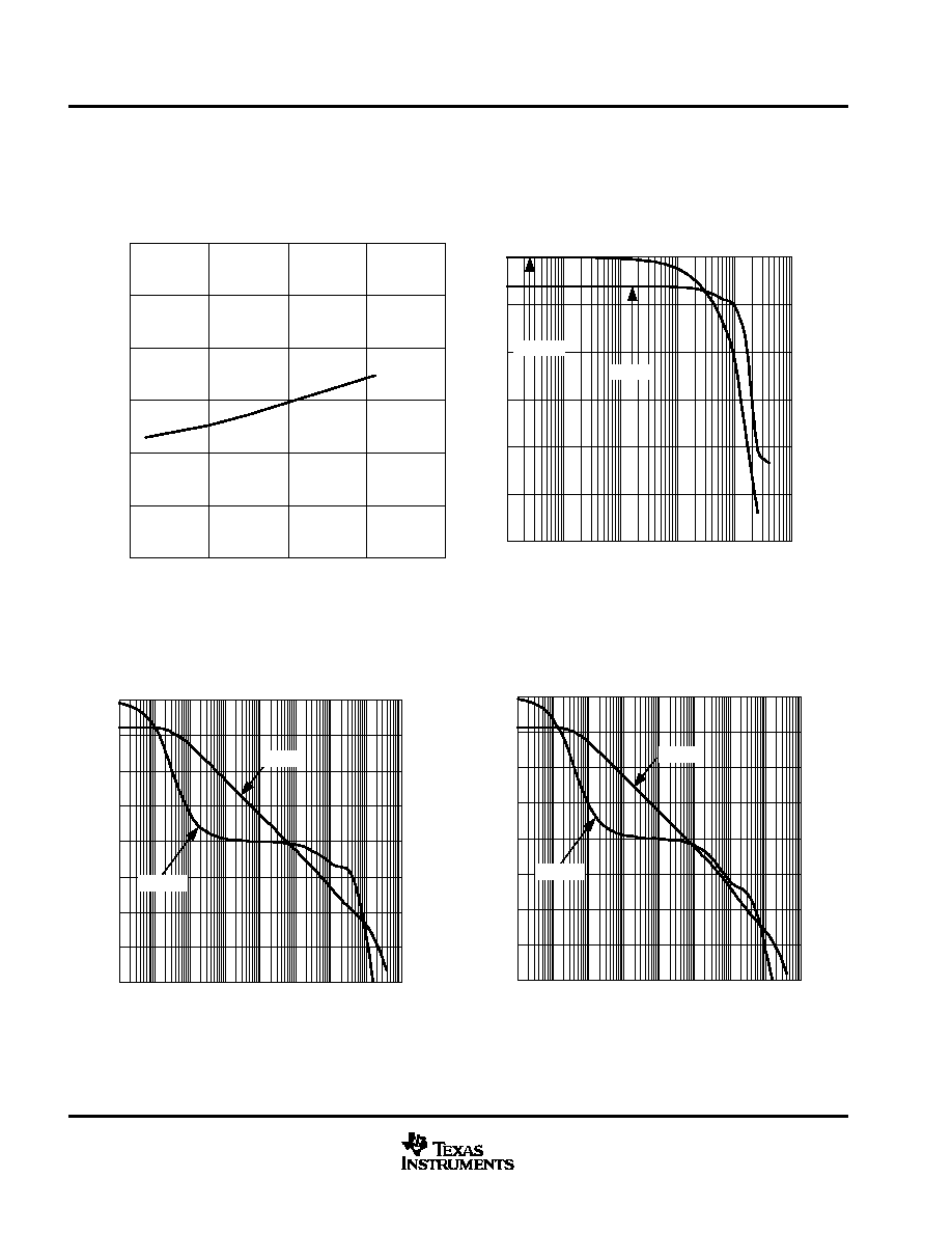
Figure 7
VVDD - Timing Resistor - k
OSCILLATOR FREQUENCY
vs
TIMING RESISTOR
f SW
- Oscillator Frequency - kHz
0
100
400
500
300
200
10
20
30
40
50
800
900
700
600
150 pF
390 pF
680 pF
270 pF
VDD, VDRV, VREF and BST pins: Modes of Operation
Depending on the available bias voltage for the UCC2541, the startup, shutdown, and restart conditions are
different. There are three distinct configurations or modes of biasing the UCC2541. The mode is detected and
latched into an internal register during power-up when VREF crosses 2 V. The register is cleared when VDD,
VDRV and VREF are simultaneously less than 1 V. A summary of the modes and their programming
requirements are listed in Table 1.
Table 1. Modes and Programming Requirements
Mode
VBIAS
Range (V)
Bias Pin
UVLO ON
(V)
UVLO OFF
(V)
Mode Requirement
at Power-Up and
VVREF = 2 V
Remarks
1
8.5 to 36
VDD [16]
VVDD = 8.5
VVDD = 8.0
V
VDD
u
V
VDRV
and V
REF
Widest line operation
2
4.75 to 8.5
VDRV [13]
VVDRV = 4.65 VVDRV = 4.3 V
VDRV
u
V
VDD
and V
REF
3
3.0 to 3.6
VREF [2]
VREF = 2.8
VREF= 2.5
V
REF
u
V
VDD
and V
VDRV
Needs regulated bias and low
VTH power MOSFETs

UCC2541
SLUS621A - AUGUST 2004 - SEPTEMBER 2005
16
www.ti.com
APPLICATION INFORMATION
VDD, VDRV, VREF and BST pins: Modes of Operation (cont.)
D
Mode 1, or normal operation requires the availability of a bias of 8.5 V or higher for the device. Here, the
bias drives the VDD pin. The low-side drive bias, V
VDRV
= 7 V, is generated from an internal linear regulator
and it directly draws current from the VDD pin. The high-side driver bias is a flying capacitor that is charged
from the VDRV pin through the G2 pin, when G2 is HI, via a diode between G2 and BST. The UCC2541
operates in Mode 1 if V
VDD
> (V
VDRV
and V
VREF
) when V
VREF
rises above 2 V. Mode 1 permits the widest
range of bias voltages, operational from 8.5 V < V
VDD
< 35 V. This mode is compatible with systems that
have a 12 V
DC
bias supply already available.
D
Mode 2 is suitable for applications where the bias is typically 5 V (between 4.5 V and 8.0 V). The bias
voltage is applied to the VDRV terminal of the UCC2541. The high-side driver bias is a flying capacitor that
is charged from the VDRV pin through the G2 pin, when G2 is HI. Bias voltage to the VDD pin is obtained
through an external voltage-doubler charge pump. If the system uses low threshold voltage power
MOSFETs, VDD can be directly tied to the VDRV pin. The bias voltage could be either a bus converter output
or an auxiliary supply.
D
Mode 3 is for synchronous buck converter applications where the bias voltage is a regulated 3.3-V source.
This is a common main output voltage in multiple output power converters. The bias voltage is applied to
the VREF pin of the UCC2541. The UCC2541 operates in Mode 3 if it detects (V
VREF
> V
VDRV
and VDD)
when V
VREF
rises above 2 V.
Assorted combinations of modes and biasing schemes are shown in Figure 7 through Figure 12. In Mode 1 and
Mode 2, the bias voltage can either be an independent auxiliary supply or it can be supplied by the power stage
voltage, as shown in Figure 7 through Figure 11. A regulated auxiliary supply must be used with Mode 3 because
the tolerance of the VREF voltage is the control tolerance of the UCC2541. In Mode 3, the regulated auxiliary
supply can be independent of the power supply input voltage (as shown in Figure 12), or the regulated auxiliary
supply can be the same source as the power supply input voltage.
UCC2541
SLUS621A - AUGUST 2004 - SEPTEMBER 2005
17
www.ti.com
APPLICATION INFORMATION
UDG-04038
Drive (7.2 V)
Regulator
VREF (3.3 V)
Regulator
Predictive
Logic
16
13
2
VDD
VDRV
VREF
BST
19
18
20
17
14
12
15
G1
SWS
SW
G2
G2S
PGND
High-Side
Driver
Low-Side
Driver
C1
D1
C2
C3
C4
Q1
Q2
UCC2541
8.5 V
VVDD
35 V
Figure 8. Mode 1 With Combined Power/Bias for Input Voltages Between 8.5 V and 35 V
Drive (7.2 V)
Regulator
VREF (3.3 V)
Regulator
Predictive
Logic
16
13
2
VDD
VDRV
VREF
BST
19
18
20
17
14
12
15
G1
SWS
SW
G2
G2S
PGND
High-Side
Driver
Low-Side
Driver
C1
D1
C2
C3
C4
Q1
Q2
AUX Bias
UCC2541
UDG-04039
8.5 V
VVDD
35 V
0 V
VIN
35 V
Figure 9. Mode 1 With Separate Power/ Bias Voltages Between 8.5 V and 35 V
UCC2541
SLUS621A - AUGUST 2004 - SEPTEMBER 2005
18
www.ti.com
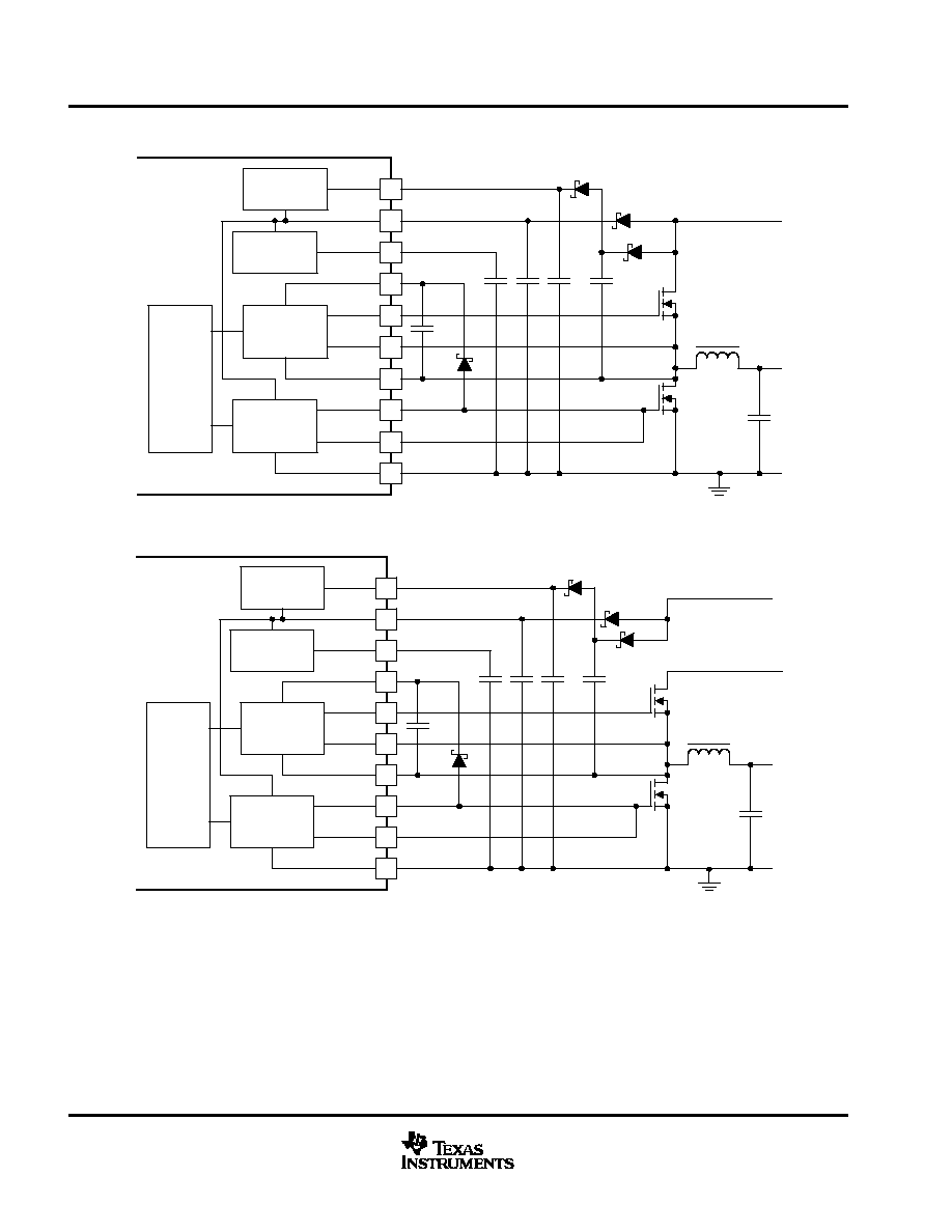
APPLICATION INFORMATION
UDG-04040
4.75 V
VVDRV
8.0 V
Drive (7.2 V)
Regulator
VREF (3.3 V)
Regulator
Predictive
Logic
16
13
2
VDD
VDRV
VREF
BST
19
18
20
17
14
12
15
G1
SWS
SW
G2
G2S
PGND
High-Side
Driver
Low-Side
Driver
C1
D1
C2
C3
C4
Q1
Q2
UCC2541
C5
D3
D2
Bias and Power
D4
Figure 10. Mode 2 With Common Bias and Power Input Voltages Between 4.75 V and 8.0 V
UDG-04041
4.75 V
VVDRV
8.0 V
0 V
VIN
35 V
Drive (7.2 V)
Regulator
VREF (3.3 V)
Regulator
Predictive
Logic
16
13
2
VDD
VDRV
VREF
BST
19
18
20
17
14
12
15
G1
SWS
SW
G2
G2S
PGND
High-Side
Driver
Low-Side
Driver
C1
D1
C2
C3
C4
Q1
Q2
AUX Bias
UCC2541
C5
D3
D2
D4
Figure 11. Mode 2 With Separate Power/ Bias (4.75 V and 8.0 V)
UCC2541
SLUS621A - AUGUST 2004 - SEPTEMBER 2005
19
www.ti.com
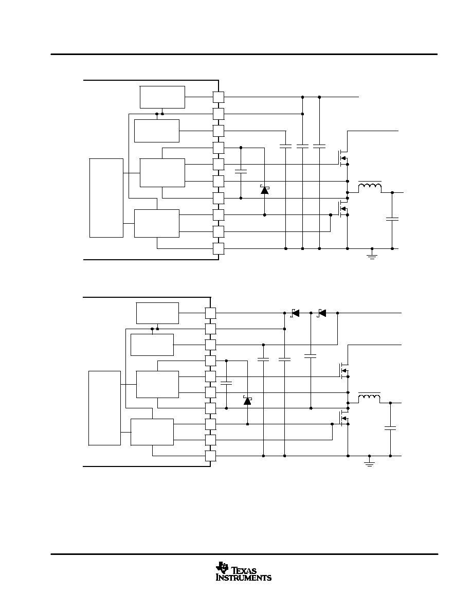
APPLICATION INFORMATION
UDG-04042
Drive (7.2 V)
Regulator
VREF (3.3 V)
Regulator
Predictive
Logic
16
13
2
VDD
VDRV
VREF
BST
19
18
20
17
14
12
15
G1
SWS
SW
G2
G2S
PGND
High-Side
Driver
Low-Side
Driver
C1
D1
C2
C3
C4
Q2
AUX Bias
UCC2541
Q1
4.75 V
VVDRV
8.0 V
0 V
VIN
35 V
(Low VTH)
(Low VTH)
Figure 12. Mode 2 With Auxiliary Biasing for Bias Voltages Between 4.75 V and 8.0 V and Logic Level or
Low Threshold Power MOSFET Transistors
UDG-04043
(Low VTH)
(Low VTH)
1.8 V
VIN
5 V
Regulated 3.3-VDC Bias
Drive (7.2 V)
Regulator
VREF (3.3 V)
Regulator
Predictive
Logic
16
13
2
VDD
VDRV
VREF
BST
19
18
20
17
14
12
15
G1
SWS
SW
G2
G2S
PGND
High-Side
Driver
Low-Side
Driver
C1
D1
C2
C4
UCC2541
C5
D3
D2
Q2
Q1
DC or Pulse Train
Figure 13. Mode 3 With Regulated 3.3-V
DC
Bias, Low Threshold Power MOSFETs
UCC2541
SLUS621A - AUGUST 2004 - SEPTEMBER 2005
20
www.ti.com
APPLICATION INFORMATION
Figure 14 illustrates a combined operational mode (referred to as Mode 4) which allows a converter operating
from intermediate bus voltages ranging from 6 V to >14 V to safely cross the boundary between Mode 1 and
Mode 2 operation. A simple circuit utilizing an NPN transistor, zener diode, and resistor allows the circuit to start
under the control of Mode 2 UVLO thresholds. Once the power stage is operational VDD is pumped up by D2
and D3 and the internal VDRV regulator raises VDRV to 7.2 V, shutting off the NPN transitor. The zener clamp
on the NPN base prevents VDRV voltage rating from being exceeded during 12-V startup. It should be noted
the circuit will run down to input voltages below 3.5 V, shutting off when VDRV has fallen to its turn-off threshold
of 4.3 V.
VIN = 6-14V
VOUT
RSET
REF
G2C
SYNCIN
GND
RAMP
VEA-
CEA-
SWS
BST
VDD
SW
G1
PGND
G2
VDRV
1
2
3
4
5
6
7
8
20
19
18
17
16
15
14
13
UCC2541
COMP
TR
G2S
SS
9
10
12
11
D1
5k
D2
D3
6.2V
Figure 14. Mode 4 Operation
UCC2541
SLUS621A - AUGUST 2004 - SEPTEMBER 2005
21
www.ti.com
APPLICATION INFORMATION
Charge Pump Capacitor Selection
Capacitors C1 through C5 are all part of a charge distribution network that allows the UCC2541 to pass charge
to the MOSFET gates of Q1 and Q2 (all reference designators in this section refer to the schematics in Figure 8
through Figure 13). This section gives guidelines on selecting the values of C1 through C5 so that the converter
functions properly. Specific capacitor values may need to be larger than the recommended value due to
MOSFET characteristics, diode D1 ≠ D4 characteristics and closed-loop converter performance. All three
modes of operation require a charge pump capacitor and diode, C1 and D1, in order to drive the high-side power
MOSFET. Modes 2 and 3 require additional charge pump capacitors and diodes in order to supply voltage to
VDD. In general, all charge pump diodes should be Schottky diodes in order to have low forward voltage and
high speed. The charge pump capacitors should be ceramic capacitors with low effective series resistance
(ESR), such as X5R or X7R capacitors.
The value of the charge pump capacitor C1 depends on the power MOSFET gate charge and capacitance, the
voltage level of the Miller plateau threshold, the forward drop of D1 and the closed-loop response time. The
unloaded high-side gate driver typically draws 2 nC of charge per rising edge plus 30
µ
A of direct current from
C1. Usually, the unloaded high-side gate driver load is miniscule compared to the gate charge requirements
of the high-side power MOSFET, Q1. Typical values for C1 are approximately 50 to 100 times the input
capacitance (C
ISS
) of MOSFET Q1. This usually allows for transient operation at extremely large duty ratio,
where C1 does not have sufficient time to fully recharge. If C1 is excessively large, its ESR and ESL prevents
it from recharging during transients, including the start-up transient.
Capacitors C2 through C5 are then selected based on the direction of charge transfer and the requirements of
the UCC2541. Selection guidelines are shown in Table 2. Keep in mind that each converter design may require
adjustments for larger capacitor ratios than those that are suggested in Table 2. The selection process begins
at the left side of Table 2 and progresses towards the right side of the table, which is the reverse order of the
charge flow during the first few cycles of start-up. If iteration is required in the design process, review the
progression of the capacitors in the order from left to right that is shown in the table.
Table 2. Charge Pump and Bias Capacitor Selection Guidelines
Mode
High-Side Drive
Capacitor (
0.1
µ
F)
VDRV Filter
Capacitor
VREF Filter
Capacitor
VDD Filter
Capacitor
VDD Charging
Capacitor
1
C1 > 50 CISS
C3 > 2
◊
C1
C2 > 0.1
µ
F
C4 > 1
µ
F
n/a
2
C1 > 50 CISS
C3 > 2
◊
C1
C2 > 0.1
µ
F
C4 > 1
µ
F, 2
◊
C3
C5 > 2
◊
C4
3
C1 > 50 CISS
C4 > 1
µ
F
2
◊
C1
C2 > 1.0
µ
F
C4 > 1
µ
F, 2
◊
C1
C5 > 2
◊
C4
For Modes 2 and 3, the VDD filter capacitor, C4, in Table 2 must supply the I
VDD
idle current to the UCC2541
(approximately 11 mA) plus the charge to drive the gates G1 and G2. Capacitor C4 must be large enough to
sustain adequate operating voltages during start-ups and other transients under the full operational I
VDD
current. Knowing the operating frequency and the MOSFET gate charges (Q
G
), the average I
VDD
current can
be estimated as:
I
VDD
+
I
VDD(idle)
)
Q
G1
)
Q
G2
f
S
D
where f
S
is switching frequency
In order to prevent noise problems, C4 must be at least 1
µ
F. Furthermore, it needs to be large enough to pass
charge along to the power MOSFET gates. Thus C4 often needs to have at least twice the capacitance of the
VDRV filter capacitor, as shown in Table 2.
(4)
UCC2541
SLUS621A - AUGUST 2004 - SEPTEMBER 2005
22
www.ti.com
APPLICATION INFORMATION
Output Stage
The UCC2541 includes dual gate drive outputs and each is capable of
±
3-A peak current. The pull-up/ pull-down
circuits of the driver are bipolar and MOSFET transistors in parallel. High-side and low-side dual drivers provide
a true 3-A high-current capability at the MOSFET's Miller Plateau switching region where it is most needed. The
peak output current rating is the combined current from the bipolar and MOSFET transistors. The output
resistance is the R
DS(on)
of the MOSFET transistor when the voltage on the driver output is less than the
saturation voltage of the bipolar transistor.
The output drivers can switch from VDD to GND. Each output stage also provides a very low impedance to
overshoot and undershoot. This means that in many cases, external-schottky-clamp diodes are not required.
The outputs are also designed to withstand 500-mA reverse current without either damage to the device or logic
upset.
For additional information on drive current requirements at MOSFET's Miller plateau region, refer to the Power
Supply Seminar SEM-1400
[3]
.
Predictive Gate Drive
TM
Technology
The Predictive Gate Drive
technology maximizes efficiency by minimizing body diode conduction. It utilizes
a digital feedback system to detect body diode conduction, and adjusts the deadtime delays to minimize the
conduction time interval. This closed loop system virtually eliminates body diode conduction while adjusting for
different MOSFETs, temperature, and load dependent delays. Since the power dissipation is minimized, a
higher switching frequency can be utilized, allowing for a smaller component size. Precise gate timing at the
nanosecond level reduces the reverse recovery time of the synchronous rectifier MOSFET body diode, which
reduces reverse recovery losses seen in the main (high-side) MOSFET. Finally, the lower power dissipation
results in increased reliability.
19 BST
20
17
18
14
G1
SWS
SW
G2
12
15
G2S
PGND
Predictive
Logic
VDRV
UDG-02149
Figure 15.
For additional information on Predictive Gate Drive
control and efficiency comparisons to earlier adaptive
delay and adaptive control techniques, refer to the Application Note SLUA285
[1]
.
UCC2541
SLUS621A - AUGUST 2004 - SEPTEMBER 2005
23
www.ti.com
APPLICATION INFORMATION
VDD and IDD
Although quiescent VDD current is low, total supply current is higher, depending on output gate drive
requirements and the programmed oscillator frequency. Total VDD current (I
VDD
) is the sum of quiescent VDD
current and the average output currents of G1 and G2, as described in equation (5). Knowing the operating
frequency and the MOSFET gate charge (Q
G
), average driver output current, per gate, can be calculated from:
I
G
+
Q
G
f
S
where
D
f
S
is switching frequency
To prevent noise problems, connect a 1-
µ
F ceramic capacitor between the VDD and GND pins. Place the 1-
µ
F
ceramic capacitor as close to the UCC2541 as possible. This capacitor is in addition to any electrolytic energy
storage capacitors that may be used in the bias supply design.
Soft-Start and Tracking Features
Separate pins are provided for the soft-start feature and the tracking feature. Soft-start or tracking (sequencing)
can be easily implemented with this configuration using a minimum number of external components. During a
power-up transient, the converter output tracks the lower of the SS voltage, the TR voltage or a 1.5-V internal
reference, provided the system is not in current limit. In other words, the voltage control loop is closed during
power-up, provided the system is not current limited. Figure 16 shows the UCC2541 configured for soft-start
operation. For applications that do not use the tracking feature, connect the TR pin to either SS or REF, as shown
in the figure. Remote shutdown and sequential power-up can be easily implemented as a transistor switch
across C
SS
.
UDG-04045
CSS
1.33
y
IRSET
1.73
y
IRSET
TR
10
11
7
SS
VEA-
UCC2541
+
+
+
+
50 mV
1.5 V
Voltage
Error
Amplifier
COMP
REF (3.3 V)
To Positive Input of
Current Error Amplifier
HUP
UVLO
+
0.7 V
Figure 16. Using the Soft-Start Feature
(5)
UCC2541
SLUS621A - AUGUST 2004 - SEPTEMBER 2005
24
www.ti.com
APPLICATION INFORMATION
The soft-start interval begins when the UCC2541 recognizes that the appropriate voltage (see Mode 1, 2 or 3)
is above the UVLO level. The voltage of C
SS
then linearly increases until it is clamped at the REF voltage of
3.3V. Regulation should be reached when the soft-start voltage reaches about 2.2 V (1.5 V plus a diode drop).
Select a C
SS
capacitor value using equation (5) to program a desired soft-start duration,
t
SS
.
C
SS
+
1.33
V
RSET
R
SET
D
t
SS
D
V
SS
+
1.33
1.5 V
R
SET
D
t
SS
2.2 V
Farads
If a UVLO fault is encountered, both outputs of the UCC2541 are disabled and the soft-start pin (SS) is
discharged to GND. The UCC2541 does not retry until the UVLO fault is cleared.
Using the TR pin, the UCC2541 can be programmed to track another converter output voltage. If the voltage
to be tracked is between 0 V and 3.3 V, simply connect the TR pin to the voltage to be tracked with a resistor
that is approximately equal to the DC impedance that is connected to the VEA- terminal (R
V1
|| R
V2
, in Figure 3).
If the voltage is above that range, use a voltage divider, again with an equivalent resistance that approximately
equals the DC impedance that is connected to the VEA- terminal. Other strategies can be used to achieve
sequential, ratiometric or simultaneous power supply tracking
[4]
.
An implementation of sequential sequencing using TPS3103K33
[2]
in a multiple output power supply
[4]
is shown
in Figure 17. Applications where the loads include a processor with a core voltage of 1.5 V and I/O ports that
require 3.3 V can require sequential sequencing in order to resolve system level bus contention problems during
start-up. In this circumstance the core must power-up first, then after an initialization period of 130 ms, the ports
are allowed to power-up. This is illustrated in Figure 18.
UDG-04061
G1
TR
G2
UCC2541
SS
From dc Power Source
VDD
TPS3103K33
GND
PFI
G1
TR
G2
UCC2541
SS
Core
1.5 V
I/O
3.3 V
REF
1.6 k
1 k
10 k
CSS
CSS
RESET
MR
PFO
Figure 17. Sequencing a Multiple Output Post Regulated Power Supply
(6)
UCC2541
SLUS621A - AUGUST 2004 - SEPTEMBER 2005
25
www.ti.com
APPLICATION INFORMATION
UDG-04061
Regulation loss due to
loss of primary line
voltage
VI/O
t - Time
1.5
0
1.43
3.3
130 ms
V - V
o
ltage - V
VCORE
Figure 18.
Using the TR pin, the UCC2541 can be programmed to ratio-metrically track another converter output voltage
[4]
.
Ratio-metric tracking is when the ratio of the output voltages is constant from zero volts to the point where one
or more of the outputs lock into regulation. The TR pin is easier to use for tracking than the SS pin because the
external currents that would be applied to the SS pin may interfere with SS discharge currents and fault recovery.
It should be understood that the voltage that is being tracked must lag the bias voltages (VDD, VDRV and REF)
on start-up and lead the bias voltages during shutdown. Furthermore, the output that is being tracked must not
reach its steady state DC level before the output that is tracking reaches its steady state DC level. Figure 18
illustrates the concept of programming an output voltage V
C
, to ratio-metrically track another output, V
M
.
UDG-04061
VC
Tracking Ratio
(Tracker)
(Tracker)
(Tracker)
(Leader)
(Leader)
(Leader)
ratio-metric
sequencing
ratio-metric
sequencing
simultaneous
sequencing
(a)
(b)
(c)
Main Power Supply
(Leader)
+
Core Power Supply
(Trader)
+
UCC2541
7
TR
VM
VM
MM
MC
MM
MC
VM
VC
VC
VM
VC
MM
MC
A
T
^
M
C
M
M
Figure 19. Ratio-Metric Tracking

UCC2541
SLUS621A - AUGUST 2004 - SEPTEMBER 2005
26
www.ti.com
APPLICATION INFORMATION
The general circuit to program the UCC2541 to track the leader supply voltage by the tracking ratio A
T
is shown
in Figure 20. To program the tracking profile gains G
T1
and G
T2
, follow the ratio-metric tracking design procedure
that is listed below. The special case of simultaneous sequencing for V
M
> 1.5V is the simplest to design; set
R
T1
= R
V1
and R
T2
= R
V2
, G
T2
is not needed. In many other cases, the circuit can be simplified with the removal
of the operational amplifier for G
T2
and the Zener clamping diode. If an operational amplifier is necessary, it
should be capable of rail to rail operation and usually low voltage bias; the TLV271 is an inexpensive solution
for both of those requirements. Notice that the tracking circuit in Figure 20 also has a soft-start capacitor, C
SS
.
The soft-start capacitor is useful for limiting the time between short-circuit retry attempts and it can prevent
overshoot when recovering from a fault that is experienced in only the tracking supply but not the main supply.
Ratio-Metric Tracking Design Procedure (see Figures 22 and 23)
1.
Determine the tracking ratio, A
T
.
A
T
+
M
C
M
M
where M
C
and M
M
are the soft-start slopes of V
C
and V
M
, respectively.
2.
Determine G
V
.
G
V
+
R
V2
R
V1
)
R
V2
where R
V2
and R
V1
are selected when designing the voltage control loop.
3.
Test G
T2
if necessary when V
M
1.5 V or A
T
G
V
> 1.
a.
If G
T2
is needed, set GT2 so that both equations (8) and (9) apply.
G
T2
+
1
)
R
F1
R
F2
so that both of the following apply:
G
T2
+
1.5 V
V
M
G
T1
and
G
T2
u
A
T
G
V
b.
If G
T2
is not needed, set G
T2
= 1.
4.
Set G
T1
.
G
T1
+
A
T
G
V
G
T2
+
R
T2
R
T1
)
R
T2
5.
Select R
T1
and R
T2
so that R
T1
|| R
T2
R
V1
|| R
V2
to minimize offset differences.
(7)
(8)
(9)
(10)
(11)

UCC2541
SLUS621A - AUGUST 2004 - SEPTEMBER 2005
27
www.ti.com
APPLICATION INFORMATION
UDG-04059
Use GT2 stage if
ATGV > 1 OR if
VMGT1
1.5 V at
steady-state
Main
Power
Supply
(Leader)
G1
TR
VEA-
G2
UCC2541
SS
CSS
3.3 V
+
0 V
Rectified Secondary Voltage
+
+
G
T2
+
1
)
R
F1
R
F2
G
T1
+
R
T2
R
T1
)
R
T2
RF2
RF1
TLV271
RT2
RT1
*DZ
*DZ needed only if VMGT1GT2 > 3 V
G
V
+
R
V2
R
V1
)
R
V2
RV2
RV1
VC
VM
nVIN
Determined by voltage loop design
Figure 20. Programming the UCC2541 to Track Another Output
More elaborate power supply sequencing and tracking can easily be implemented by extending the above
techniques. Consult Reference [4] for further information.
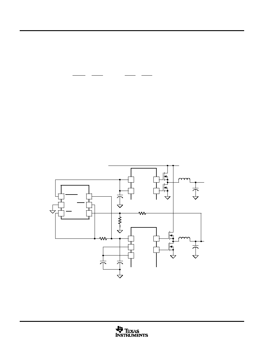
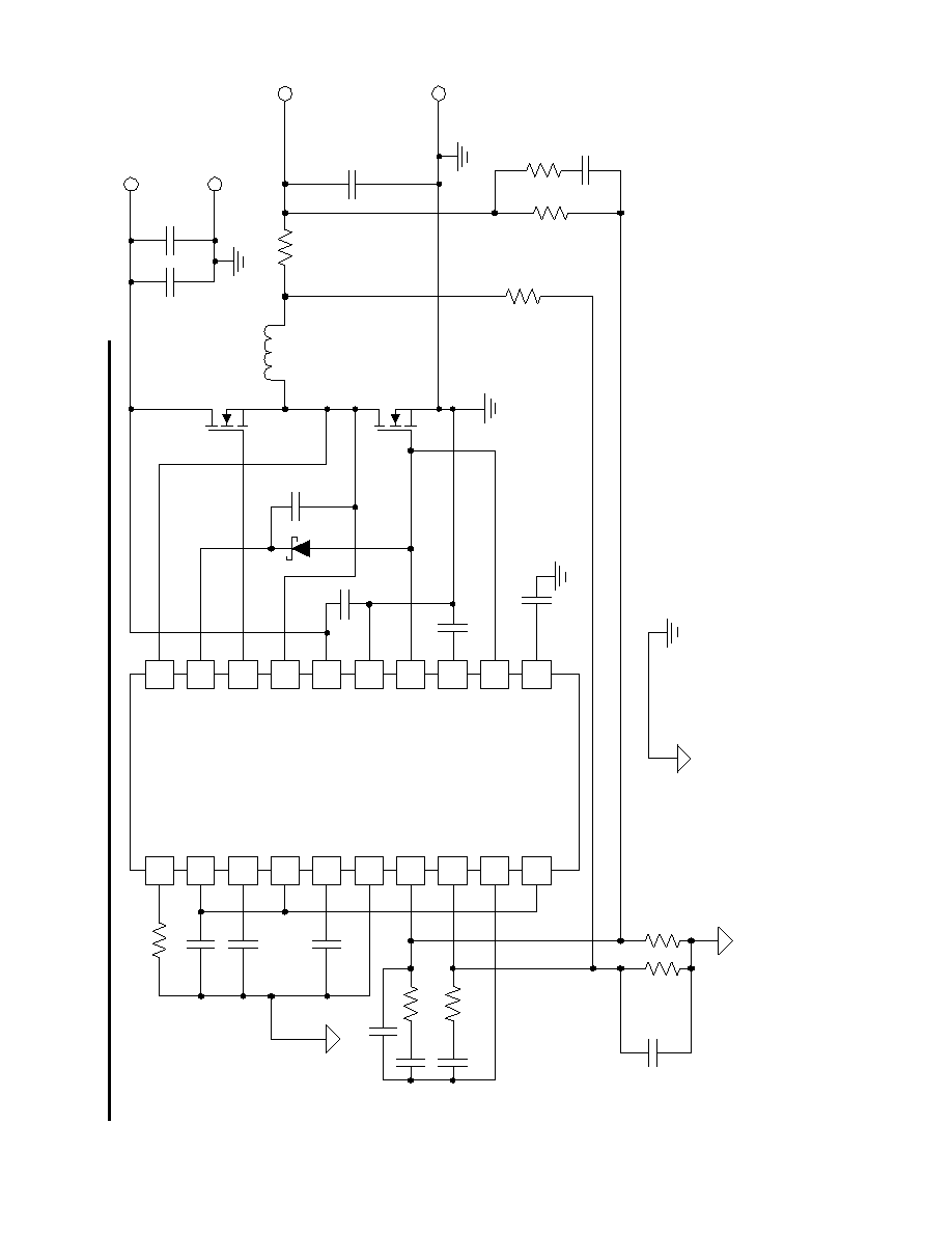
The following schematic shows an example POL (point of load) converter capable of delivering 20 A at 2.5 V
from an unregulated IBC (intermediate bus converter) providing 9 V to14 V. In this application, the UCC2541
is configured to operate in Mode 1, and the converter turns ON when the UCC2541 UVLO threshold of 8.5 V
is exceeded. The upper input voltage rating is limited by the MOSFET and capacitor voltage ratings, not the
UCC2541. For lower current requirements from 10 A to15 A a single lower MOSFET would suffice.

UCC2541
SLUS621A - AUGUST 2004 - SEPTEMBER 2005
28
www.ti.com
APPLICATION INFORMATION
17.8k
2.2uH
2 x 330uF
POSCAP
26.7k
26.7k
17.8k
1uF
8.2k
15k
0.1uF
10k
VIN=9-14V
VOUT=2.5V
RSET
REF
G2C
SYNCIN
GND
RAMP
VEA-
CEA-
SWS
BST
VDD
SW
G1
PGND
G2
VDR
V
1
2
3
4
5
6
7
8
20
19
18
17
16
15
14
13
UCC2541
COMP
TR
G2S
SS
9
10
12
11
0.0032
22uF
1N5819
680pF
470pF
3.3nF
6.8nF
0.18uF
0.39uF
0.22uF
1nF
270pF
2.2nF
787
22uF
Q1:
HA
T2168H
Q2: 2 x
HA
T2165H
GND and PGND tied together under
IC through PowerP
AD
Figure 21. 20-A POL (Point of Load) Converter
UCC2541
SLUS621A - AUGUST 2004 - SEPTEMBER 2005
29
www.ti.com
APPLICATION INFORMATION
In the 20-A converter the output current is sensed by R4. The UCC2541 limits output current when the C
EA
-
(pin 8) exceeds the V
EA
- (pin 7) by 50 mV. To select the current sense resistor the 50-mV signal must be gained
up by the reciprocal of the output feedback divider ratio given by:
R8
R8
)
R9
+
R12
R12
)
R10
For this 2.5-V output, the divider ratio is 0.6, and the following calculation can determine the typical voltage
across the sense resistor to begin current limit operation:
V
RSNS
+
V
R4
+
1
0.6
50 mV
+
83.3 mV
The peak inductor ripple current should also be considered in R
SNS
selection, and is 1/2 the peak-to-peak
inductor current calculated during the OFF-time of the converter:
dI
PP
1
f
S
*
V
O
V
IN
f
S
V
O
L
+
3 A
PP
with V
O
=2.5 V, V
IN
=12 V, f
S
=300 kHz, and L1=2.2
µ
H. In this design IL1, peak =21.5 A.
For a 20-A converter with current limiting at 20% overload the sense resistor can be calculated as:
R
SNS
+
V
RSNS
1.2
IL
PEAK
+
83.3 mV
1.2
21.5 A
+
3.2 m
W
With this value of sense resistor the average power dissipation can be calculated to be:
P
RSNS
+
I
OUT
2
R
SNS
+
20 A
2
3.2 m
W +
1.28 W
Low value current sense resistors are commonly available in 1-W surface mount packages, so two packages
should be paralleled to meet the power dissipation requirements in high current designs, and the final value used
will be a compromise of available components. In surface mount applications a Kelvin connection to the sense
resistor is not easily attainable, so the connection resistance from the sense resistors to the PCB must be
included in the effective sense resistance.
The voltage and current feedback component magnitudes were ratioed according to the discussion in section,
COMP, VEA- AND CEA- pin: Voltage and Current Error Amplifiers. In this application, the optional component
CFIR was not needed. However, a 1-nF capacitor (CST in Figure 3) was needed to filter the C
EA
- signal to allow
the converter to start at turn on and to restart after current limit hiccup operation.
(12)
(13)
(14)
(15)
(16)

UCC2541
SLUS621A - AUGUST 2004 - SEPTEMBER 2005
30
www.ti.com
THERMAL INFORMATION
The useful temperature range of a controller that contains high-current output drivers is greatly affected by the
drive power requirements of the load and the thermal characteristics of the device package. In order for a power
driver to be useful over a particular temperature range the package must allow for the efficient removal of the
heat produced while keeping the junction temperature within rated limits. The UCC2541 is available in the 20-pin
HTSSOP PowerPAD
t
package and also the 32-pin QFN PowerPAD
TM
package.
The PowerPAD
TM
offers the most effective means of removing the heat from the semiconductor junction and
therefore long term reliability improvement. As illustrated in [5], the PowerPAD packages offer a leadframe die
pad that is exposed at the base of the package. This pad is soldered to the copper on the PC board directly
underneath the device package, reducing the
jc down to 2
∞
C/W. Data is presented in [5] to show that the power
dissipation can be quadrupled in the PowerPAD
t
configuration when compared to the standard packages. The
PC board must be designed with thermal lands and thermal vias to complete the heat removal subsystem, as
summarized in [6] to realize a significant improvement in heat-sinking over standard non-PowerPAD
t
surface
mount packages.
TYPICAL CHARACTERISTICS
Figure 22
TJ - Junction Temperature -
∞
C
V
VREF
- Reference V
o
ltage - V
OUTPUT REFERENCE VOLTAGE
vs
TEMPERATURE
-50
3.25
3.20
0
3.35
3.30
3.40
50
100
150
-325
-315
-285
-295
-275
-50
0
50
100
150
-305
Figure 23
RAMP CURRENT
vs
TEMPERATURE
I RAMP
- Ramp Current -
µ
A
TJ - Junction Temperature -
∞
C
RRSET = 10 k
UCC2541
SLUS621A - AUGUST 2004 - SEPTEMBER 2005
31
www.ti.com
TYPICAL CHARACTERISTICS
0.5
-50
0
50
100
150
0.6
1.0
0.9
1.1
0.8
0.7
Figure 24
TJ - Junction Temperature -
∞
C
µ
A/
µ
A
I
G2C
/I
RAMP
AND I
SS
/I
RAMP
vs
TEMPERATURE
IG2C/IRAMP, RRSET = 10 k
IG2C/IRAMP, RRSET = 50 k
ISS/IRAMP, RRSET = 10 k
ISS/IRAMP, RRSET = 50 k
6.8
7.6
7.4
7.2
7.0
-50
0
50
100
150
Figure 25
REGULATOR OUTPUT VOLTAGE
vs
TEMPERATURE
V
VDR
V
- Regulator Output V
o
ltage - V
TJ - Junction Temperature -
∞
C
MODE 1
Figure 26
TJ - Junction Temperature -
∞
C
OSCILLATOR FREQUENCY
vs
TEMPERATURE
200
300
550
500
600
450
400
350
-50
0
50
100
150
250
f SW
- Oscillator Frequency - kHz
C = 450 pF
C = 270 pF
Figure 27
CURRENT ERROR AMPLIFIER OFFSET
vs
TEMPERATURE
V
CEA-
- Current Error Amplifier Offset V
oltage -
m
V
TJ - Junction Temperature -
∞
C
45
47
53
55
51
49
-50
0
50
100
150
UCC2541
SLUS621A - AUGUST 2004 - SEPTEMBER 2005
32
www.ti.com
TYPICAL CHARACTERISTICS
Figure 28
TJ - Junction Temperature -
∞
C
V
SYNCHIN
-
T
iming
Signal
V
oltage - V
SYNCIN THRESHOLD VOLTAGE
vs
TEMPERATURE
1.50
1.55
1.75
1.70
1.80
1.65
1.60
-50
0
50
100
150
5
0
-5
-25
-10
-15
10 k
100 M
1 k
1 M
-90
-45
-180
-135
0
-225
-270
100 k
10 M
-20
Phase
Gain
f - Frequency - Hz
INVERTING AMPLIFIER GAIN AND PHASE
vs
FREQUENCY
Gain -
d
B
Phase -
∞
Figure 29
20
100
80
120
60
40
0
-20
-40
100
1 k
10 M 100 M
10
-90
-45
-180
-135
0
100 k 1 M
10 k
1
Figure 30
f - Frequency - Hz
CURRENT ERROR AMPLIFIER GAIN AND PHASE
vs
FREQUENCY
Phase
Gain
Gain -
d
B
Phase -
∞
120
-90
-45
-180
-135
0
100
1 k
10 M 100 M
10
100 k 1 M
10 k
1
20
100
80
60
40
0
-20
-40
Figure 31
VOLTAGE ERROR AMPLIFIER GAIN AND PHASE
vs
FREQUENCY
f - Frequency - Hz
Phase
Gain
Gain - dB
Phase -
∞
UCC2541
SLUS621A - AUGUST 2004 - SEPTEMBER 2005
33
www.ti.com
TYPICAL CHARACTERISTICS
Figure 32
VVDD - Bias Voltage - V
OPERATING CURRENT (DC)
vs
BIAS VOLTAGE
I VDD
- Bias Current - mA
5
15
25
30
40
0
35
10
20
0
2
12
10
8
6
4
Figure 33. Predictive Gate Drive - G2 Falling
t - Time - 20 ns/div
5.0 V/div.
5.0 V/div.

UCC2541
SLUS621A - AUGUST 2004 - SEPTEMBER 2005
34
www.ti.com
RELATED PRODUCTS
D
UCC27223 High Efficiency Predictive Synchronous Buck Driver with Enable
D
UCC2540 High-Efficiency Secondary-Side Synchronous Buck PWM Converter
D
TPS40070/1 High-Efficiency Midrange Input Synchronous Buck Controller With Voltage Feed-Forward
REFERENCES
1.
Application Note, Predictive Gate Drive
E
FAQ, by Steve Mappus (SLUA285)
2.
Datasheet, TPS3103K33 Ultra-Low Supply Current/Supply Voltage Supervisory Circuits, (SLVS363)
3.
Power Supply Seminar SEM-1400 Topic 2: Design And Application Guide For High Speed MOSFET Gate
Drive Circuits, by L. Balogh, (SLUP133)
4.
Power Supply Seminar SEM1600 Topic 2: Sequencing Power Supplies in Multiple Voltage Rail
Environments, by D. Daniels, D. Gehrke, and M. Segal, (SLUP224)
5.
Technical Brief, PowerPAD Thermally Enhanced Package, (SLMA002)
6.
Application Brief, PowerPAD Made Easy, (SLMA004)
35
www.ti.com

36
www.ti.com
37
www.ti.com
TR
SS
10
11
17.8k
2.2uH
2 x 330uF
POSCAP
26.7k
26.7k
17.8k
1uF
8.2k
15k
0.1uF
10k
VIN=9-14V
VOUT=2.5V
RSET
REF
G2C
SYNCIN
GND
RAMP
VEA-
CEA-
SWS
BST
VDD
SW
G1
PGND
G2
VDR
V
1
2
3
4
5
6
7
8
20
19
18
17
16
15
14
13
UCC2541
COMP
TR
G2S
SS
9
10
12
11
0.0032
22uF
1N5819
680pF
470pF
3.3nF
6.8nF
0.18uF
0.39uF
0.22uF
1nF
270pF
2.2nF
787
22uF
Q1:
HA
T2168H
Q2: 2 x
HA
T2165H
GND and PGND tied together under
IC through PowerP
AD

39
www.ti.com
PACKAGING INFORMATION
Orderable Device
Status
(1)
Package
Type
Package
Drawing
Pins Package
Qty
Eco Plan
(2)
Lead/Ball Finish
MSL Peak Temp
(3)
UCC2541PWP
ACTIVE
HTSSOP
PWP
20
70
Green (RoHS &
no Sb/Br)
CU NIPDAU
Level-2-260C-1 YEAR
UCC2541PWPG4
ACTIVE
HTSSOP
PWP
20
70
Green (RoHS &
no Sb/Br)
CU NIPDAU
Level-2-260C-1 YEAR
UCC2541PWPR
ACTIVE
HTSSOP
PWP
20
2000 Green (RoHS &
no Sb/Br)
CU NIPDAU
Level-2-260C-1 YEAR
UCC2541PWPRG4
ACTIVE
HTSSOP
PWP
20
2000 Green (RoHS &
no Sb/Br)
CU NIPDAU
Level-2-260C-1 YEAR
UCC2541RHBR
ACTIVE
QFN
RHB
32
3000 Green (RoHS &
no Sb/Br)
CU NIPDAU
Level-2-260C-1 YEAR
UCC2541RHBT
ACTIVE
QFN
RHB
32
250
Green (RoHS &
no Sb/Br)
CU NIPDAU
Level-2-260C-1 YEAR
(1)
The marketing status values are defined as follows:
ACTIVE: Product device recommended for new designs.
LIFEBUY: TI has announced that the device will be discontinued, and a lifetime-buy period is in effect.
NRND: Not recommended for new designs. Device is in production to support existing customers, but TI does not recommend using this part in
a new design.
PREVIEW: Device has been announced but is not in production. Samples may or may not be available.
OBSOLETE: TI has discontinued the production of the device.
(2)
Eco
Plan
-
The
planned
eco-friendly
classification:
Pb-Free
(RoHS)
or
Green
(RoHS
&
no
Sb/Br)
-
please
check
http://www.ti.com/productcontent
for the latest availability information and additional product content details.
TBD: The Pb-Free/Green conversion plan has not been defined.
Pb-Free (RoHS): TI's terms "Lead-Free" or "Pb-Free" mean semiconductor products that are compatible with the current RoHS requirements
for all 6 substances, including the requirement that lead not exceed 0.1% by weight in homogeneous materials. Where designed to be soldered
at high temperatures, TI Pb-Free products are suitable for use in specified lead-free processes.
Green (RoHS & no Sb/Br): TI defines "Green" to mean Pb-Free (RoHS compatible), and free of Bromine (Br) and Antimony (Sb) based flame
retardants (Br or Sb do not exceed 0.1% by weight in homogeneous material)
(3)
MSL, Peak Temp. -- The Moisture Sensitivity Level rating according to the JEDEC industry standard classifications, and peak solder
temperature.
Important Information and Disclaimer:The information provided on this page represents TI's knowledge and belief as of the date that it is
provided. TI bases its knowledge and belief on information provided by third parties, and makes no representation or warranty as to the
accuracy of such information. Efforts are underway to better integrate information from third parties. TI has taken and continues to take
reasonable steps to provide representative and accurate information but may not have conducted destructive testing or chemical analysis on
incoming materials and chemicals. TI and TI suppliers consider certain information to be proprietary, and thus CAS numbers and other limited
information may not be available for release.
In no event shall TI's liability arising out of such information exceed the total purchase price of the TI part(s) at issue in this document sold by TI
to Customer on an annual basis.
PACKAGE OPTION ADDENDUM
www.ti.com
21-Nov-2005
Addendum-Page 1
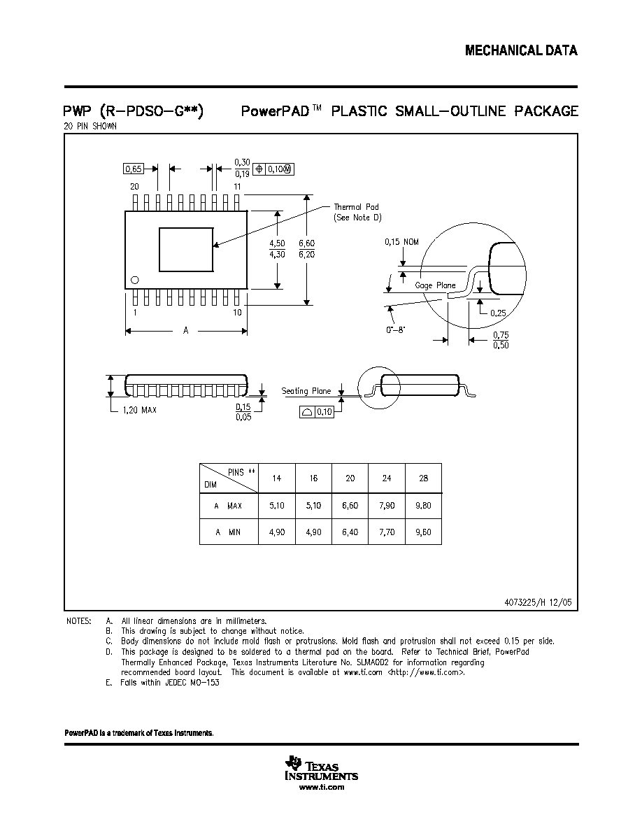
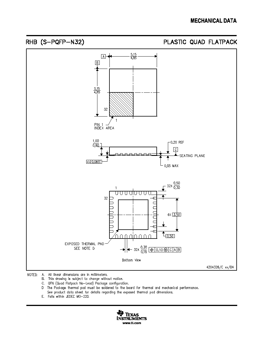

IMPORTANT NOTICE
Texas Instruments Incorporated and its subsidiaries (TI) reserve the right to make corrections, modifications,
enhancements, improvements, and other changes to its products and services at any time and to discontinue
any product or service without notice. Customers should obtain the latest relevant information before placing
orders and should verify that such information is current and complete. All products are sold subject to TI's terms
and conditions of sale supplied at the time of order acknowledgment.
TI warrants performance of its hardware products to the specifications applicable at the time of sale in
accordance with TI's standard warranty. Testing and other quality control techniques are used to the extent TI
deems necessary to support this warranty. Except where mandated by government requirements, testing of all
parameters of each product is not necessarily performed.
TI assumes no liability for applications assistance or customer product design. Customers are responsible for
their products and applications using TI components. To minimize the risks associated with customer products
and applications, customers should provide adequate design and operating safeguards.
TI does not warrant or represent that any license, either express or implied, is granted under any TI patent right,
copyright, mask work right, or other TI intellectual property right relating to any combination, machine, or process
in which TI products or services are used. Information published by TI regarding third-party products or services
does not constitute a license from TI to use such products or services or a warranty or endorsement thereof.
Use of such information may require a license from a third party under the patents or other intellectual property
of the third party, or a license from TI under the patents or other intellectual property of TI.
Reproduction of information in TI data books or data sheets is permissible only if reproduction is without
alteration and is accompanied by all associated warranties, conditions, limitations, and notices. Reproduction
of this information with alteration is an unfair and deceptive business practice. TI is not responsible or liable for
such altered documentation.
Resale of TI products or services with statements different from or beyond the parameters stated by TI for that
product or service voids all express and any implied warranties for the associated TI product or service and
is an unfair and deceptive business practice. TI is not responsible or liable for any such statements.
Following are URLs where you can obtain information on other Texas Instruments products and application
solutions:
Products
Applications
Amplifiers
amplifier.ti.com
Audio
www.ti.com/audio
Data Converters
dataconverter.ti.com
Automotive
www.ti.com/automotive
DSP
dsp.ti.com
Broadband
www.ti.com/broadband
Interface
interface.ti.com
Digital Control
www.ti.com/digitalcontrol
Logic
logic.ti.com
Military
www.ti.com/military
Power Mgmt
power.ti.com
Optical Networking
www.ti.com/opticalnetwork
Microcontrollers
microcontroller.ti.com
Security
www.ti.com/security
Telephony
www.ti.com/telephony
Video & Imaging
www.ti.com/video
Wireless
www.ti.com/wireless
Mailing Address:
Texas Instruments
Post Office Box 655303 Dallas, Texas 75265
Copyright
2005, Texas Instruments Incorporated