 | –≠–ª–µ–∫—Ç—Ä–æ–Ω–Ω—ã–π –∫–æ–º–ø–æ–Ω–µ–Ω—Ç: UCC2585 | –°–∫–∞—á–∞—Ç—å:  PDF PDF  ZIP ZIP |
UCC2585
UCC3585
PRELIMINARY
DESCRIPTION
The UCC2585/UCC3585 synchronous Buck controller provides flexible
high efficiency power conversion for output voltages as low as 1.25V with
guaranteed
±1% DC accuracy. Output currents are only limited by the
choice of external logic level MOSFETs. With an input voltage range of
2.5V to 6.0V it is the ideal choice for 3.3V only, battery input, or other low
voltage systems. Applications include local microprocessor core voltage
power supplies for desktop and Notebook computers, and high speed GTL
bus regulation. Its fixed frequency oscillator is capable of providing practical
PWM operation to 700kHz.
With its low voltage capability and inherent "always on" operation, the
UCC2585/UCC3585 causes VOUT to track VIN once VIN has exceeded
the threshold voltage of the external P channel MOSFET. Tracking can be
tailored for any application with a single resistor or disabled by connecting
TRACK to VIN. For dual supply rail microprocessors this feature negates
the need for external diodes to insure supply voltage tracking between the
+3.3V and lower voltage microprocessor core supplies.
(continued)
Low Voltage Synchronous Buck Controller
FEATURES
∑
Resistor Programmable 1.25V to 4.5V
V
OUT
∑
2.5V to 6V Input Supply Range
∑
1% DC Accuracy
∑
High Efficiency Synchronous
Switching
∑
Drives P-channel (High Side) and
N-channel (Low Side) MOSFETs
∑
Lossless Programmable Current Limit
∑
Logic Compatible Shutdown
∑
Programmable Frequency
∑
Start-up Voltage Tracking Protects
Dual Rail Microprocessors
07/99
12
14
6
11
8
PDRV
CLSET
ISENSE
13
5
9
NDRV
PWRGND
TRACK
N/C
1
4
10
2
15
VIN
VFB
ENB
COMP
SD
16
7
3
SS
GND
CT
ISET
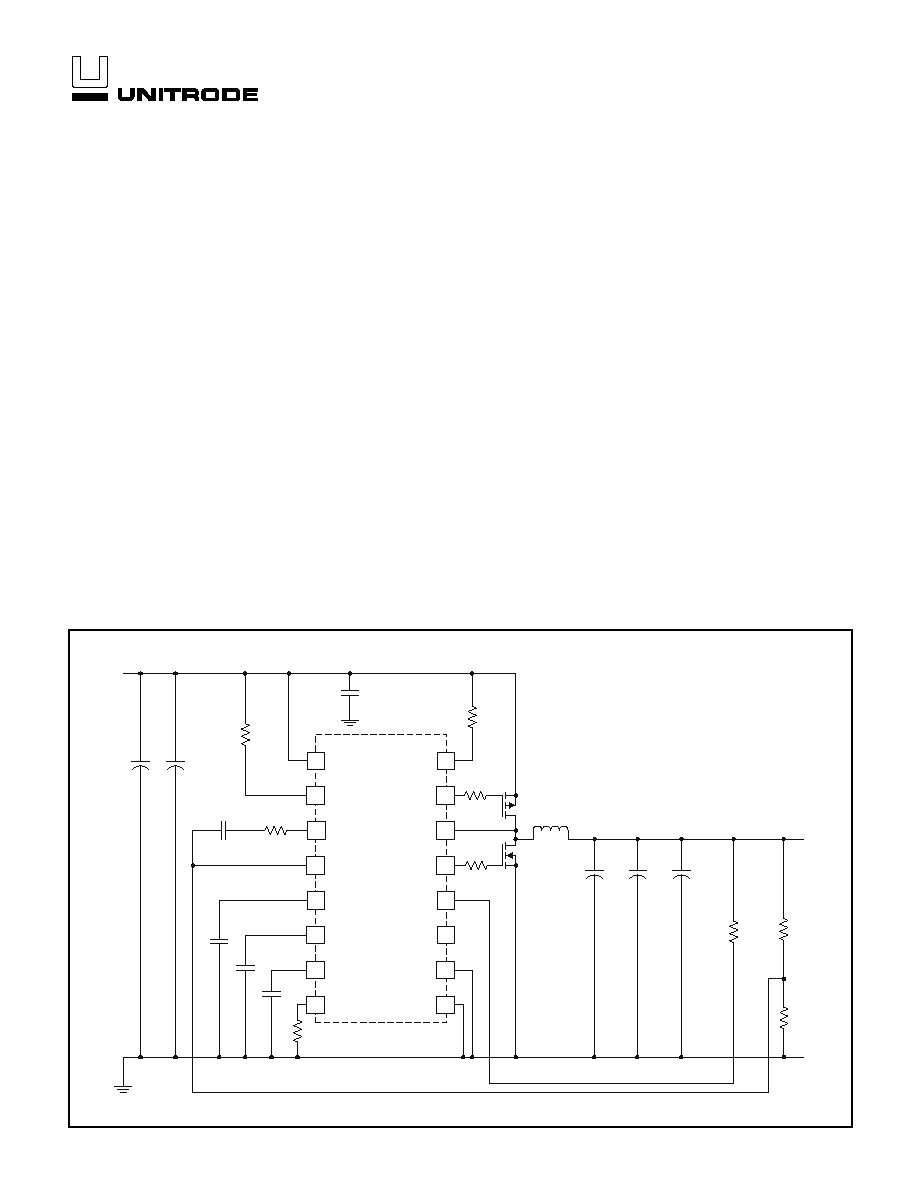
C8
0.47
µ
F
Q1
IRF7404
Q2
IRF7401
L1 4.7
µ
F
C9
220
µ
F
C10
220
µ
F
C11
VOUT
RTN
RTN
VIN
220
µ
F
+
+
+
R4
100k
R2
549k
R6
3
R5
3
R1
10k
R3
27.4k
R12
32k
R10
36k
R11
82k
C6
470pF
C5
0.22
µ
F
C4
3.2N
C7
147pF
C1
150
µ
F
C2
150
µ
F
+
+
TYPICAL APPLICATION DIAGRAM
UDG-98024
2
UCC2585
UCC3585
DIL-16, SOIC-16, SSOP-16 (TOP VIEW)
J, N, D, and M Packages
ABSOLUTE MAXIMUM RATINGS
Analog Pins
Minimum and Maximum Forced Voltage
(Reference to GND) . . . . . . . . . . . . . . . . . . . ≠0.3V to +6.3V
Digital Pins
Minimum and Maximum Forced Voltage
(Reference to GND) . . . . . . . . . . . . . . . . . . . . .≠0.3V to 6.3V
Power Driver Output Pins
Maximum forced current . . . . . . . . . . . . . . . . . . . . . . . . .
±
1.0A
Operating Junction Temperature . . . . . . . . . . ≠55∞C to +125∞C
Storage Temperature. . . . . . . . . . . . . . . . . . . ≠65∞C to +150∞C
Note: Unless otherwise indicated, voltages are reference to
ground and currents are positive into, negative out of, the spec-
ified terminals. Pulsed is defined as a less than 10% duty cycle
with a maximum duration of 500ns.
NDRV
VIN
CT
PWRGND
PDRV
SD
ISENSE
N/C
1
2
3
4
5
6
7
8
16
15
14
13
12
11
10
9
COMP
ENB
CLSET
TRACK
ISET
SS
VFB
GND
CONNECTION DIAGRAMS
DESCRIPTION (cont.)
The UCC2585/UCC3585 drives a complementary pair of
power MOSFET transistors, P-channel on the high side,
and N-channel on the low side to step down the input
voltage at up to 90% efficiency.
A programmable two-level current limiting function is pro-
vided by sensing the voltage drop across the high side P
channel MOSFET. This circuit can be configured to pro-
vide pulse-by-pulse limiting, timed shutdown after 7 con-
secutive faults, or latch-off after fault detection, allowing
maximum application flexibility. The current limit thresh-
old is programmed with a single resistor selected to
match system MOSFET characteristics.
The UCC2585/UCC3585 also includes undervoltage
lockout, a logic controlled enable, and softstart functions.
The UCC2585/UCC3585 is offered in the 16 pin surface
mount and through hole packages.
APPLICATIONS
∑
Low Voltage Microprocessor Power such as PowerPC
603 and 604
∑
High Power 5V or 3.3V to 1.25V≠4.5V Regulators
∑
GTL Bus Termination
3
UCC2585
UCC3585
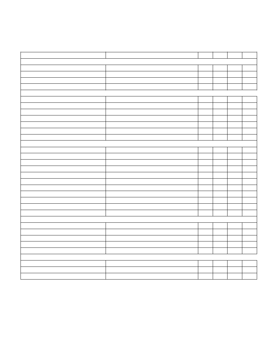
ELECTRICAL CHARACTERISTICS:
Unless otherwise stated, these specifications hold for T
A
= 0∞C to 70∞C for the
UCC3585, and T
A
= ≠40∞C to 85∞C for the UCC2585. T
A
= T
J
. VIN = 3.3V, ENB, I
SENSE
= V
IN
, V
FB
= 1.25V, COMP = 1.5V,
C
T
= 330pF, R
ISET
= 100k, RTRACK = 10k, RCLSET = 10k.
PARAMETER
TEST CONDITIONS
MIN
TYP
MAX
UNITS
Input Supply Section
Supply Current ≠ Total (Active)
2.3
3.5
mA
Supply Current ≠ Shutdown
ENABLE = 0V
10
25
µ
A
VIN Turn On Threshold (UVLO)
2.35
2.60
V
VIN Turn On Hysteresis
450
550
mV
Voltage Amplifier Section
Input Voltage (Internal Reference)
T
A
= 0∞C to 70∞C, VIN = 3.0V to 3.6V, Note 1
1.238
1.250
1.262
V
Input Voltage (Internal Reference)
VIN = 3.0V to 3.6V, IND/MIL Temp, Note 1
1.228
1.250
1.273
V
Open Loop Gain
COMP = 0.5 to 2.5V
65
80
dB
Output Voltage High
I(COMP) = ≠50
µ
A
3.00
3.25
V
Output Voltage Low
I(COMP) = 50
µ
A
0.10
0.25
V
Output Source Current
≠100
≠175
µ
A
Output Sink Current
0.4
1.0
mA
Oscillator/PWM Section
Initial Accuracy
T
J
= 25∞C
405
450
495
kHz
Initial Accuracy
Over Temperature
390
450
510
kHz
CT Ramp Peak to Valley
1.8
2.1
2.4
V
CT Ramp Valley Voltage
0.3
0.4
V
PWM Maximum Duty Cycle
COMP = 3V, Measured on PDRV
100
%
PWM Minimum Duty Cycle
COMP = 0.2V, Measured on PDRV
0
%
PWM Delay to Outputs
COMP = 2.5V
45
ns
Tracking Current
Measured on TRACK, V
TRACK
= 1.6V
10
12
15
µ
A
Enable High Threshold
Measured on ENABLE (Note 3)
2.8
V
Enable Low Threshold
Measured on ENABLE
0.5
V
Softstart Charge Current
SS = 0V
≠10
≠14
≠18
µ
A
Current Limit Section
Pulse to Pulse Threshold
Measured Between V
IN
and I
SENSE
100
125
150
mV
CLSET Current
11
14
16
µ
A
SD Sink Current
SD = 2V
8
13
18
µ
A
SD Source Current
SD = 2V
≠100
≠140
µ
A
Restart Threshold
Measured on SDOWN
0.40
0.55
0.90
V
Output Driver Section (PDRV, NDRV)
Pull Up Resistance
≠100mA (Source) T
A
= 25
∞
C
6
Pull Down Resistance
100mA (Sink) T
A
= 25
∞
C
4
Deadtime Delay
Note 2
150
200
250
ns
Note 1. Measured on COMP with the Error Amp in a Unity Gain (voltage follower) configuration.
Note 2. 50% point of PDRV Rise to NDRV Rise and 50% point of NDRV Fall to PDRV Fall.
Note 3. Enable High Threshold = V
IN
≠0.5.

4
UCC2585
UCC3585
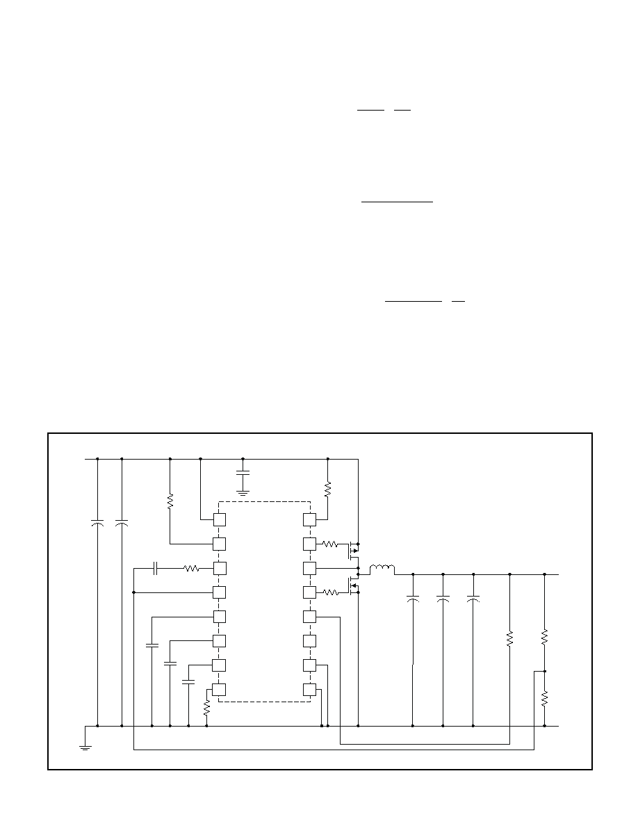
11
16
10
CURENT
LIMIT ADJ
8
CLSET
SD
ISENSE
DISABLE DRIVERS
CURRENT
LIMIT
PRECISION
BIAS SET
7
12 PDRV
DRIVER
ANTI
SHOOT THRU
14 NDRV
DRIVER
6
15
ISET
TRACK
VIN
1
ENB
VIN
≠0.8V
1.25V
REF
1.25V
UVLO
2V
2
COMP
4
VFB
1.25V
3
SS
10
µ
A
9
NC
OSCILLATOR
PWM
PRECISION
BIAS
OVER CURRENT COUNTER
SHUTDOWN TIMER
CT
13 PWRGND
SOFTSTART COMPLETE
10
µ
A
5
GND
UVLO
ENABLE
L = NO SHUTDOWN
H = LATCHED SHUTDOWN
CAP = TIMED SHUTDOWN
10
µ
A
R
Q
Q
S
PWM
LATCH
D
REVERSE
CURRENT
LOGIC
SOFTSTART COMPLETE
H = NO OVERCURRENT
TRACK
CLK
TRACK
UVLO
REVERSE
REVERSE
BLOCK DIAGRAM
PIN DESCRIPTIONS
CLSET: CLSET is used to program the pulse by pulse
and overcurrent shutdown levels for the UCC1585. A re-
sistor is connected between CLSET and VIN to set the
thresholds. The threshold follows the following relation-
ship:
lcl
R
R
RDS on
ISET
CLSET
=
∑
1 25
.
(
)
COMP: Output of the Voltage type error amplifier. Loop
compensation
components
are
connected
between
COMP and VFB.
CT: A high quality ceramic capacitor connected between
this pin and ground sets the PWM oscillator frequency by
the following relationship:
F
CT
=
∑
1
6700
(
)
Use capacitor values greater than 100pF in order to mini-
mize the effects of stray capacitance. The oscillator is ca-
pable of reliable operation in excess of 1MHz.
ENB: A LOGIC1 (V
IN
≠0.5V) on this input will activate the
Output drivers. A logic zero (0.5V) will prevent switching
of the output drivers. Do not allow ENB to remain be-
tween these levels steady state.
GND: Reference level for the IC. All voltages and cur-
rents are with respect to GND.
ISENSE: ISENSE performs two functions. The first is to
monitor the voltage dropped across the high side P chan-
nel MOSFET switch while it is conducting. This informa-
tion is used to detect over current conditions by the
current limit circuitry. The second function of ISENSE is
to measure current through the lowside N-channel
MOSFET. When the current flow through this MOSFET is
drain to source, (i.e. reversed), this FET is turned off for
the remainder of the switching cycle.
UDG-98008

5
UCC2585
UCC3585
ISET: A resistor is connected between ISET and ground
to
program
a
precision
bias
for
many
of
the
UCC2585/UCC3585 circuit blocks. Allowable resistor val-
ues are 90k
to 110k
.
1.25V is provided to ISET via a
buffered version the internal bandgap voltage reference.
The resultant current is 1.25V / R
ISET.
This current is mir-
rored directly over to CLSET to program the over current
thresholds. A second use for this current is to set a basis
for the charging current of the oscillator.
PDRV: High current driver output for the high side P
channel MOSFET switch. A 3
to 10
series resistor be-
tween PDRV and the MOSFET gate may be inserted to
reduce ringing on this pin. In some layout situations, a
low V
F
diode may be required from this pin to ground to
keep the pin from ringing more than 0.5V below ground.
PWRGND: High current return path for the MOSFET
drivers. PWRGND and GND should be terminated to-
gether as close to the IC package as possible.
SD: This pin can configure current limit to operate in any
one of three different ways.
1) A forced voltage of less than 250mV on SD inhibits the
shutdown function causing pulse by pulse limiting.
2) A capacitor from SD to GND provides a control-
ler-converter shutdown timeout after 7 consecutive
overcurrent signals are received by the current limit cir-
cuitry. An interval 10
µ
A (typ) current source discharges
the SD capacitor to the 0.5V (typ) restart threshold. The
shutdown time is given by:
(
)
[
]
T
C
V
A
SHUT
SD
IN
=
∑
-
0 5
10
.
µ
,
where C
SD
is the value of the capacitor from SD to GND,
and VIN is the chip supply voltage (on pin 15). At this
point, a softstart cycle is initiated, and a 100
µ
A current
(typ) quickly recharges SD to VIN. During softstart, pulse
by pulse limiting is enabled, and the 7 cycle count is de-
layed until softstart is complete (i.e. charged to approxi-
mately VIN volts).
3) A forced voltage of greater than 1V on SD will cause
the UCC2585/UCC3585 to latch OFF after 7 overcurrent
signals are received. After the controller is latched off, SD
must drop below 250mV to restart the controller.
SS: A low leakage capacitor connected between SS and
GND will provide a softstart function for the converter.
The voltage on this capacitor will slowly charge on start-
up via an internal current source. The output of the Volt-
age error amplifier (COMP) tracks this voltage thereby
limiting the controller duty ratio.
NDRV: High current driver output for the low side
MOSFET switch. A 3
to 10
series resistor between
NDRV and the MOSFET gate may be inserted to reduce
ringing on this pin. In some layout situations, a low V
F
di-
ode may be required from this pin to ground to keep the
pin from ringing more than 0.5V below ground.
TRACK: A resistor is connected between TRACK and
output voltage of the converter to set the start-up profile
of the power converter. Certain dual supply rail micropro-
cessors require that a maximum voltage differential be-
tween the supply rails is not exceeded. Failure to do so
results in large currents in the microprocessor through
the ESD (electrostatic discharge) protection devices. This
can result in chip failure. The UCC2585/UCC3585 is de-
signed such that it is "normally on" before V
IN
reaches
the 2.0V (nom.) UVLO threshold. That is, the high side P
channel MOSFET switch driver output is actively held low
allowing the MOSFET to conduct current to the output as
soon as V
IN
is high enough to exceed the gate turn on
threshold. The resistor from TRACK to V
OUT
sets the
voltage level on VOUT at which the P channel MOSFET
is turned off. The tracking cutoff voltage follows the fol-
lowing relationship:
(
)
V
V
A
R
OUT
TRACK
(max)
.
=
+
∑
1 25
12
µ
This is necessary for very low output voltage applications
(< 2.0V), where overvoltage may occur if the Pchannel
MOSFET is not disabled before the UVLO threshold is
reached. For applications with V
OUT
greater than 2.0V,
TRACK can be disabled by tying TRACK to V
IN
.
VFB: Inverting input to the Voltage type error amplifier.
The common mode input range for VFB extends from
GND to 1.5V.
VIN: Supply voltage for the UCC2585/UCC3585.Bypass
with a 0.1
µ
F ceramic capacitor (minimum) to supply the
switching transient currents required by the external
MOSFET switches.
PIN DESCRIPTIONS (cont.)
6
UCC2585
UCC3585
Some of today's microprocessors require very low oper-
ating voltages. In some cases, as low as 1.8V of supply
voltage are required in addition to already available 3.3V
system voltage. Following is an illustration of a design
using the UCC3585 as the power controller.
The design criteria are as follows:
∑
Input Voltage (V
IN
) 3.3V DC
∑
Output Voltage (V
OUT
) 1.8V DC
∑
Output Ripple Voltage (V
OUT
) 18mV
∑
Output Current (I
OUT
) 3.5A DC
Other features include
∑
Output Tracking
∑
Switching Frequency (F
S
) 350kHz
∑
100% Surface Mount
The first few steps in the design are to define the power
stage (Schematic Fig. 1).
1) The normal operating duty cycle (
) of the regulator is
approximately
=
=
=
V
V
OUT
IN
1 8
3 3
0 545
.
.
.
2) Select the output inductor to meet ripple current re-
quirements. For this design, the allowable ripple current in
the output inductor is selected to be 10% of the full load
output current.
L
V
V
F
I
H
IN
OUT
S
OUT
1
0 1
4 6
=
∑
∑
∑
=
-
(
)
.
.
µ
A Pulse Engineering SMT inductor (PE-53682) is 4.7
µ
H
has a DC resistance (R
L1
) of 8.3m
and will dissipate
0.1W under full load operation.
The resulting
I
OUT
is now:
I
V
V
F
A
OUT
IN
OUT
S
=
-
∑
∑
=
-
(
)
.
.
4 7 10
0 5
6
3) Next, the output capacitors are determined based
upon the output ripple criteria. Assuming the ripple is lim-
ited by the equivalent series resistance, or ESR, of the
capacitors and not the impedance of the capacitors at the
switching frequency, then the output capacitor selection is
based upon ESR, size and voltage considerations.
APPLICATION INFORMATION
12
14
6
11
8
PDRV
CLSET
ISENSE
13
5
9
NDRV
PWRGND
TRACK
N/C
1
4
10
2
15
VIN
VFB
ENB
COMP
SD
16
7
3
SS
GND
CT
ISET
C8
0.47
µ
F
Q1
IRF7404
Q2
IRF7401
L1 4.7
µ
F
C9
220
µ
F
C10
220
µ
F
C11
VOUT
RTN
RTN
VIN
220
µ
F
+
+
+
R4
100k
R2
549k
R6
3
R5
3
R1
10k
R3
27.4k
R12
32k
R10
36k
R11
82k
C6
470pF
C5
0.22
µ
F
C4
3.2N
C7
147pF
C1
150
µ
F
C2
150
µ
F
+
+
Figure 1. Application circuit schematic.
UDG-98024

7
UCC2585
UCC3585
ESR
V
I
OUT
OUT
=
=
=
0 018
0 5
0 026
.
.
.
A 220
µ
F, 6.3V Sprague 594D capacitor has an ESR of
75m
. Three of these in parallel will result in an overall
ESR of 25m
. (C9, C10, and C11 in Fig. 1). Since the
output ripple current is so low, the capacitor's ripple cur-
rent rating of 1.45A is not a concern.
To check the assumption that the capacitor's impedance
at the switching frequency is dominated by the ESR and
not the capacitor's capacitance value, calculate the im-
pedance and compare it to the ESR.
Z
F
C
k
m
C
S
=
∑
∑
=
∑
∑
=
1
2
1
2
350
220
2
µ
The ESR of the capacitor is 37 times that of the imped-
ance of the capacitor at the switching frequency, so the
earlier assumption was valid.
4) Before selecting the switching MOSFETs, the current
that will be flowing through them must first be deter-
mined.
I
I
I
A
D
OUT
OUT
PK
=
=
+
2
3 8
.
The RMS of this current in Q1 is
I Q
I
A
D
RMS
D
PK
1
2 8
=
=
.
And in Q2
I Q
I
A
D
RMS
D
PK
2
1
2 5
=
- =
.
5) Since this regulator must be able to operate from a
3.3V source, the MOSFETs used must have a gate
threshold level of no more than 2V.
For Q1, an IRF7404 is selected. It has an R
DS(on)
of
0.04
, a total gate charge (Q
G
1) of 50nC, and a turn
OFF (t
OFF
1) time of 65ns. The conduction loss in Q1 will
be:
P Q
I Q
R
Q
W
D
ON
D
RMS
DS
ON
1
1
1 0 593
2
=
∑
=
.
The gate drive losses will be
P Q
Q
V
F
mW
D
GATE
G
IN
S
1
58
1
=
∑
∑
=
And finally the turn OFF losses are estimated
P Q
V
I Q
T
F
W
D
OFF
IN
D
PK
OFF
S
1
1
2
1
0 14
1
= ∑
∑
∑
∑
=
.
The total power loss for Q1 is the sum of these three:
P Q
W
D
TOTAL
1
0 5
=
.
6) Q2 has been selected to be an IRF7401, which has an
R
DS(ON)
of 0.03
, and a total gate charge (Q
G
2) of 48nC
and a body diode turn OFF switching time (t
OFF
2) of
59ns. In this topology, the N Channel MOSFET, Q2, is
turned OFF prior to the turn ON of Q1, so when Q2 is
turned OFF, current is being re-routed from the channel
of the device into the intrinsic body diode. Therefore Q2's
intrinsic body diode incurs switching loss during the turn
OFF interval.
The conduction loss in Q2 is:
P Q
I Q
R
Q
W
D
ON
D
RMS
DS
ON
2
2
2 0 2
2
=
∑
=
.
The gate drive losses will be
P Q
Q
V
F
mW
D
GATE
G
IN
S
2
55
2
=
∑
∑
=
And the body diode turn OFF loss:
P Q
V
I
T
F
W
D
D OFF
IN
D
OFF
S
PK
2
1
2
0 13
2
_
.
= ∑
∑
∑
∑
=
The total power loss for Q2 is the sum of these three:
P Q
W
D
TOTAL
2
0 4
=
.
7) Thus far the power loss in the two MOSFETs and the
output inductor total 1.0W. The average input current is:
I
V
I
P
V
A
IN
OUT
OUT
LOSS
IN
AVG
=
∑
+
=
2 2
.
The peak to peak ripple in the input capacitors is the
peak current less the average input current during Q1's
ON time, and equal to the average input current during
Q1's OFF time. The RMS value of this current is then:
I
I
I
I
A
IN CAP
D
IN
IN
RMS
PK
AVG
AVG
_
(
)
(
)
(
)
.
=
-
∑ +
∑ - =
2
2
1
1 9
8) After the input capacitor's input ripple current is
known, select the input capacitors. Again, Sprague 594D
Solid Tantalum capacitors are chosen. A single 150
µ
F,
10V capacitor has a ripple current rating of 1.35A RMS.
Two in parallel (C1 and C2) will have a combined capabil-
ity of 2.7A, and a total ESR of 40m
. The losses in the
capacitors are:
P
I
ESR
W
DIN CAP
IN CAP
RMS
_
_
.
=
∑
=
2
0 14
Adding the capacitor loss to that previously found, the to-
tal losses are now 2.1W.
9) The overall efficiency of the power train is then
E
V
I
V
I
FF
OUT
OUT
OUT
OUT
=
∑
∑
+
=
2 1
0 84
.
.
The losses are dominated by the MOSFETs Q1 and Q2.
One way to improve the efficiency would be to reduce the
conduction loss in Q1, either by choosing a device with a
APPLICATION INFORMATION (cont.)

8
UCC2585
UCC3585
lower R
DS(on)
or by paralleling it with another MOSFET.
The conduction losses in Q2 may be improved by the
same technique, but will prove detrimental in switching
losses. To lower the switching losses, Q2 may be paral-
leled with a Schottky diode. In this manner, the switching
loss may be absorbed by the Schottky, instead of the
MOSFET.
10) After the power stage design is completed, attention
is given to the feedback loop. The LC filter gain is de-
scribed by the equation (10A) below: (where
= j2
f
)
Where C
OUT
is the combined capacitance of C9, C10,
and C11 and R
ESR
is the ESR of the capacitors.
There will be a double pole at:
F
L
C
kHz
P
OUT
=
∑
=
1
2
1
2 8
.
and a zero at the point where the impedance of the out-
put capacitors equals the ESR:
F
R
C
kHz
Z
ESR
OUT
=
∑
∑
=
1
2
9 6
.
The modulator gain is given by
K
V
V
PWM
IN
RAMP
=
=
1 65
.
where V
RAMP
is the peak to peak amplitude of the oscil-
lator ramp found on the CT pin. The overall open loop
gain is shown in Fig. 2.
11) The voltage divider is next determined to give us the
proper output voltage. First select one of the divider re-
sistors R11 = 82k. The other resistor becomes:
R
R
V
V
R
k
OUT
REF
10
11
11 36
=
∑
-
=
12) The equation for the error amplifier in this configura-
tion is:
K
C
R
R
EA
J
=
∑ ∑
+
1
2
7
2
10
f
For a gain of 5 and a zero at 2kHz
R
R
k
2 15
10 180
=
∑
=
and
C
fp R
pF
7
1
2
2
440
=
∑
∑
=
The overall voltage loop gain now has a crossover at
34kHz with a phase margin of about 73 degrees.
13) Select the R
ISET
resistor, R3, to be 100k. (The range
of value should be between 90k and 110k.) Then choos-
ing the current limit trip point to be 130% of I
OUT
, the cur-
rent limit set resistor is then found by the relationship
(
)
R
I
R
Q
R
k
OUT
DS on
ISET
3
1 3
1 25
1
27 2
=
∑
∑
∑
=
.
.
.
Note that the R
DS(on)
value used should include the ef-
fects of temperature.
APPLICATION INFORMATION (cont.)
-40
-30
-20
-10
0
10
10
100
1000
10000
100000
FREQUENCY (Hz)
GAIN
(dB)
Figure 2. Modulator and filter frequency response.
(10A)
KLC
R
C
L
C
R
C
R
C
ESR
OUT
OUT
L
OUT
ESR
OUT
=
+ ∑
∑
+
∑ ∑
+
∑
+
∑
+
1
1
1
2
1
L
R
LOAD
1
-60
-40
-20
0
20
40
60
80
100
10
100
1000
10000
100000
FREQUENCY (Hz)
GAIN
(dB)
AMPLIFIER GAIN
OVERALL LOOP GAIN
Figure 3. Error amp and closed loop frequency
response.

9
UCC2585
UCC3585
14) During normal power on of the UCC3585, the gate of
Q1 is held low (Q1 turned ON) until the V
CC
input to the
IC reaches the 2V Under Voltage Lockout (UVLO) volt-
age. At UVLO, the UCC3585 wakes up and switching be-
gins on Q1 and Q2. With a 1.8V output however, the
output will reach 2V before regulation begins! This is
where the tracking function comes into use. By selecting
an appropriate resistive divider from the output, we can
select the point below UVLO at which Q1 will be shut off.
Upon reaching UVLO, the UCC3585 will then begin to
regulate normally.
With a 1.8V nominal output voltage, select the tracking
turn off point to be 1.6V.
R
k
3
1 6 1 25
12
29
=
-
=
.
.
µ
Note that the tracking function ONLY makes a difference
below UVLO. If V
OUT
were to be 2V or above, then the
tracking pin should be tied to V
IN
.
15) A capacitor on the SD pin will allow the converter to
shutdown in the event seven consecutive over current
pulses occur. If a timing shutdown interval of 1ms is cho-
sen as the shutdown time, T
SD
, then the value of the ca-
pacitor is:
C
T
V
I
I
nF
SD
IN
CHG
DICHG
4
0 5
1
1
3 2
=
∑
+
=
(
≠ . )
.
Where I
CHG
and I
DISCHG
are 100
µ
A and 10
µ
A respect-
fully.
16) The next step is to find the value of timing capacitor.
C
T
pF
S
6
6000
476
=
=
A 470pF capacitor will result in a switching frequency of
354kHz.
17) The softstart capacitor is selected for a 5ms startup
time. Knowing that a 10
µ
A current source will charge the
capacitor to 2.5V, the softstart capacitor is given by:
C
T
I
V
m
nF
SS
CHG
SS
5
5
10
2 5
20
=
∑
=
∑
=
µ
.
APPLICATION INFORMATION (cont.)
1.0
0.5
1.5
2.0
V
OUT
(V
)
1.0
1.5
2.0
2.5
V
IN
(V)
POWER ON PROFILE
WITHOUT "TRACK AND HOLD"
POWER ON
PROFILE WITH
"TRACK AND HOLD"
Figure 5. Power on profile.
0
45
90
135
180
10
100
1000
10000
100000
FREQUENCY (Hz)
PHASE
(
DEG
R
EES)
ERROR AMP
OVERALL LOOP
Figure 4. Error amp and closed loop frequency
response.
40
20
80
1.2
1.4
1.6
1.8
V
TR
(V)
R
T
k
60
2.0
Figure 6. Tracking resistor value as a function of turn
off voltage.
UNITRODE CORPORATION
7 CONTINENTAL BLVD. ∑ MERRIMACK, NH 03054
TEL. (603) 424-2410 ∑ FAX (603) 424-3460
PowerPC is a registered trademark of International Business
Machines Corporation

IMPORTANT NOTICE
Texas Instruments and its subsidiaries (TI) reserve the right to make changes to their products or to discontinue
any product or service without notice, and advise customers to obtain the latest version of relevant information
to verify, before placing orders, that information being relied on is current and complete. All products are sold
subject to the terms and conditions of sale supplied at the time of order acknowledgement, including those
pertaining to warranty, patent infringement, and limitation of liability.
TI warrants performance of its semiconductor products to the specifications applicable at the time of sale in
accordance with TI's standard warranty. Testing and other quality control techniques are utilized to the extent
TI deems necessary to support this warranty. Specific testing of all parameters of each device is not necessarily
performed, except those mandated by government requirements.
CERTAIN APPLICATIONS USING SEMICONDUCTOR PRODUCTS MAY INVOLVE POTENTIAL RISKS OF
DEATH, PERSONAL INJURY, OR SEVERE PROPERTY OR ENVIRONMENTAL DAMAGE ("CRITICAL
APPLICATIONS"). TI SEMICONDUCTOR PRODUCTS ARE NOT DESIGNED, AUTHORIZED, OR
WARRANTED TO BE SUITABLE FOR USE IN LIFE-SUPPORT DEVICES OR SYSTEMS OR OTHER
CRITICAL APPLICATIONS. INCLUSION OF TI PRODUCTS IN SUCH APPLICATIONS IS UNDERSTOOD TO
BE FULLY AT THE CUSTOMER'S RISK.
In order to minimize risks associated with the customer's applications, adequate design and operating
safeguards must be provided by the customer to minimize inherent or procedural hazards.
TI assumes no liability for applications assistance or customer product design. TI does not warrant or represent
that any license, either express or implied, is granted under any patent right, copyright, mask work right, or other
intellectual property right of TI covering or relating to any combination, machine, or process in which such
semiconductor products or services might be or are used. TI's publication of information regarding any third
party's products or services does not constitute TI's approval, warranty or endorsement thereof.
Copyright
©
1999, Texas Instruments Incorporated