 | –≠–ª–µ–∫—Ç—Ä–æ–Ω–Ω—ã–π –∫–æ–º–ø–æ–Ω–µ–Ω—Ç: UCC2751N | –°–∫–∞—á–∞—Ç—å:  PDF PDF  ZIP ZIP |

UCC2751
UCC3751
DESCRIPTION
The UCC3751 controller is designed for driving a power stage that gener-
ates low frequency, high voltage sinusoidal signals for telephone ringing
applications. The controller and the power stage are most suitable for sin-
gle line applications where low cost, high efficiency and minimum parts
count are critical. In addition to providing the sinusoidal ringing signal, the
controller and the power stage are designed to provide the required DC
voltage across the output when the phone goes off-hook. The DC voltage is
also added as the offset to the ringing signal. This feature eliminates the
need to have a separate talk battery voltage power supply as well as relays
and drivers to switch between the ringing voltage and the talk battery.
The UCC3751 directly drives primary side switches used to implement a
push-pull resonant converter topology and transformer coupled sampling
switches located on the secondary of the converter. For normal ring signal
generation, the primary switching frequency and secondary sampling fre-
quency are precisely offset from each other by the ringing frequency to pro-
duce a high voltage low frequency alias signal at the output. The off-hook
condition is detected by sensing the AC current and when AC limit is ex-
ceeded, the sampling frequency is set to be equal to the primary switching
frequency to produce a DC output.
The drive signal frequencies are derived from a high frequency (3579545
Hz) crystal. The primary switching frequency is 89.488 kHz and the sam-
pling frequency is 20, 25 or 50 Hz less depending on the status of fre-
quency select pins FS0 and FS1.
Single Line Ring Generator Controller
FEATURES
∑
Novel Topology for Low-Cost, Efficient
Generation of Ring Voltage
∑
Provides DC Offset and "Talk Battery"
Voltage for Off-Hook Conditions
∑
Selectable 20, 25 and 50 Hz Ring
Frequency
∑
Secondary (AC) Current Limiting
Allows Removal of AC Voltage under
Off-Hook Conditions
∑
Primary Current Limiting to turn Power
Stage off under Fault Conditions
∑
Operates from a Single 12V Supply
APRIL 1999 - REVISED AUGUST 2000 - SLUS267B
1
10
15
4
ENABLE
VDD
DELAY
XTAL2
6
OHD
2
RINGEN
12
DRVS
9
VS12
5
11
13
DRV1
DCLIM
DRV2
16
XTAL1
8
FS1
7
FS0
14
PGND
3
GND
C
BYP2
SAMPLING
CIRCUIT
C
F
AC SIGNAL
V
OUT
V
1
C
R2
12V
C
DC
D1
DC SIGNAL
Q1
L
IN
V
IN
12V
T1
L
R
L
R
N:1
Q2
R
SENSE
UCC3751
3.579545MHz
C
R1
C
BYP1
TYPICAL APPLICATIONS CIRCUIT
UDG-98047
The circuits described in this datasheet are covered under US Patent #5,663,878 and other patents pending.
2
UCC2751
UCC3751
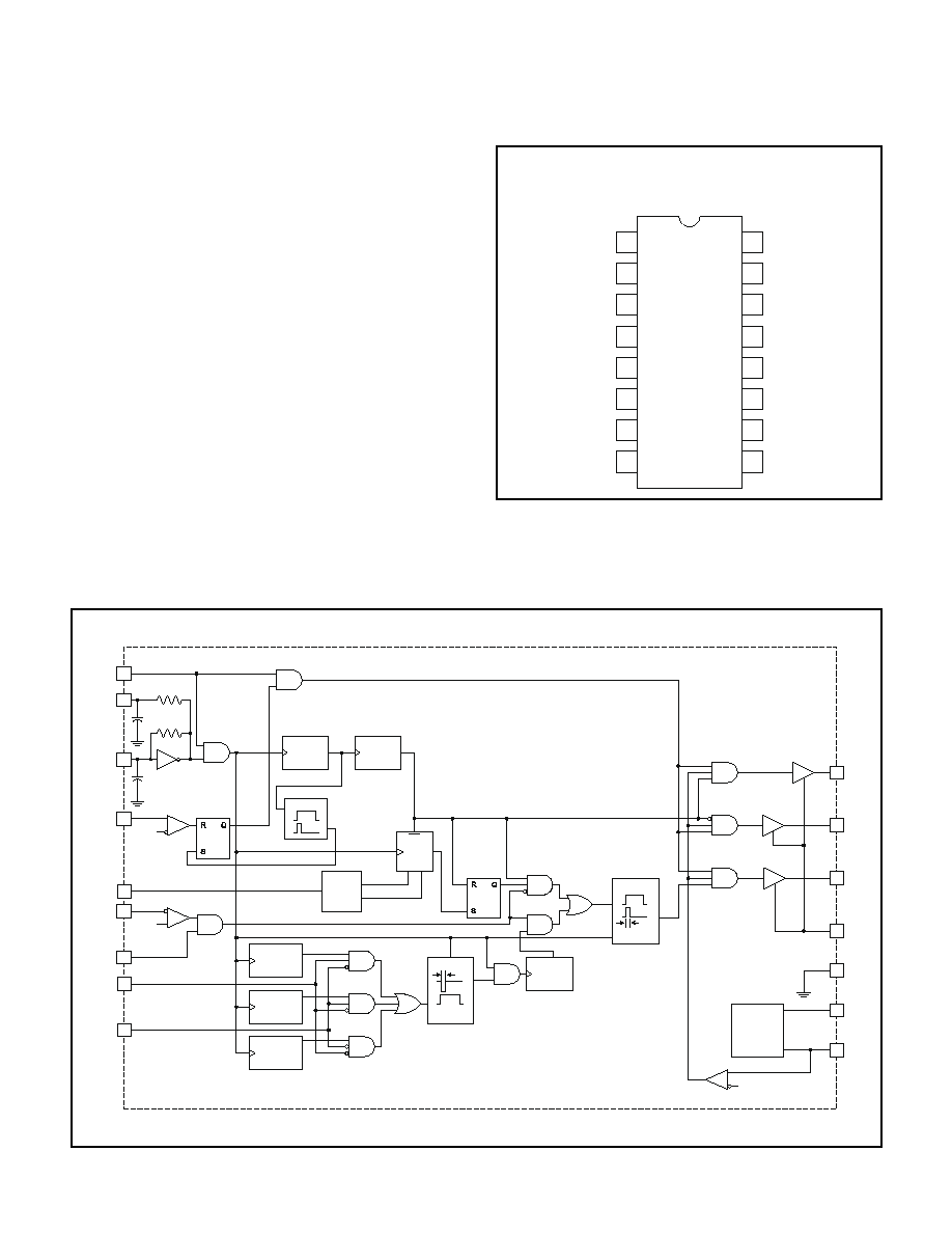
DIL-16, SOIC-16 (TOP VIEW)
N or D Packages
ABSOLUTE MAXIMUM RATINGS
Input Supply Voltage . . . . . . . . . . . . . . . . . . . . . . . . . . . . . 14V
Analog Inputs (OHD, DCLIM, XTAL1, XTAL2)
Maximum Forced Voltage. . . . . . . . . . . . . . . . . . . . ≠0.3 to 5V
Logic Inputs
Maximum Forced Voltage . . . . . . . . . . . . . . . . . . ≠0.3 to 7.5V
Reference Output Current (V
DD)
. . . . . . . . . . . Internally Limited
Output Current (DRV1, DRV2, DRVS) Pulsed . . . . . . . . . . 1.5A
Operating Junction Temperature . . . . . . . . . . ≠55∞C to +125∞C
Storage Temperature . . . . . . . . . . . . . . . . . . . ≠65∞C to +150∞C
Note: Unless otherwise indicated, voltages are referenced to
ground and currents are positive into, negative out of, the spe-
cific terminals. Pulsed is defined as a less than 10% duty cycle
with a maximum duration of 500 S.
PGND
XTAL2
XTAL1
DRV2
DRVS
ENABLE
DRV1
VS12
1
2
3
4
5
6
7
8
16
15
14
13
12
11
10
9
RINGEN
DELAY
FS1
OHD
FS0
GND
V
DD
DCLIM
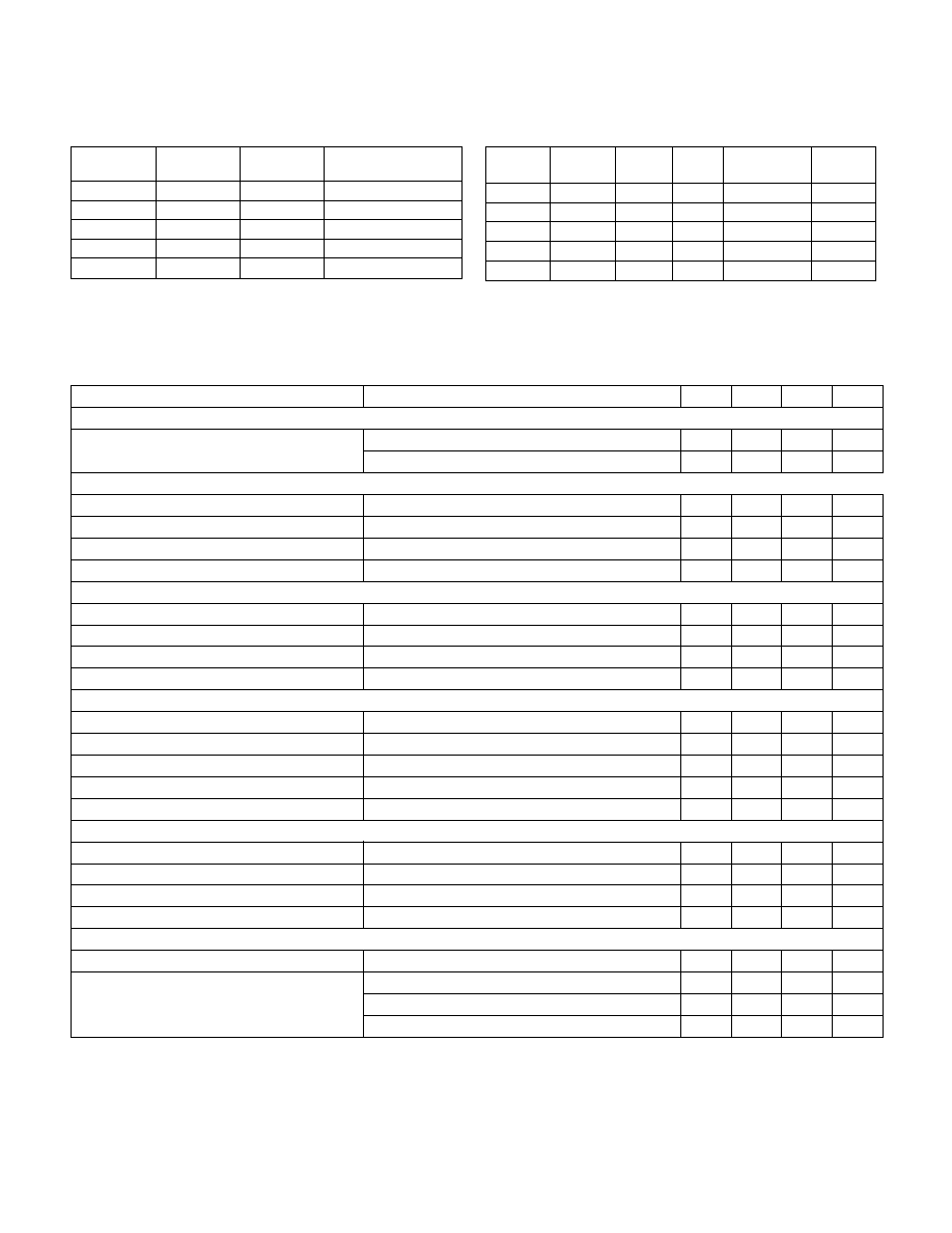
CONNECTION DIAGRAM
11
4
13
OHD
DRV1
RINGEN
14
9
3
12
DELAY
FS0
FS1
2
6
1
DRVS
VDD
GND
VS12
7
8
DRV2
PGND
5 VOLT
REFERENCE
ONE-SHOT
1/F
OSC
4.5V
CLR
CLK
PROGRAMMABLE
COUNTER
MODULO
40
COUNTER
MODULO
3,560
COUNTER
MODULO
1,800
COUNTER
MODULO
4,480
COUNTER
2/F
OSC
ONE-SHOT
2 BIT
A/D
300mV
DCLIM
5
300mV
XTAL1
16
XTAL2
15
10
MODULO
2
COUNTER
ENABLE
MODULO
20
COUNTER
ONE-SHOT
BLOCK DIAGRAM
UDG-98020
3
UCC2751
UCC3751
ELECTRICAL CHARACTERISTICS:
Unless otherwise stated, these specifications hold for T
A
= 0∞C to 70∞C for the
UCC3751 and ≠40∞C to +85∞C for the UCC2751, T
A
= T
J
.
PARAMETER
TEST CONDITIONS
MIN
TYP
MAX
UNITS
V12 Supply Current Section
Supply Current
ENABLE = 0V
1.0
3.0
mA
ENABLE = 5V
1.0
3.0
mA
Internal Reference with External Bypass Section
Output Voltage (VDD)
4.85
5
5.15
V
Load Regulation
0mA
IV
DD
2mA
5
20
mV
Line Regulation
10V < VS12 < 13V, I
VDD
= 1mA
3
20
mV
Short Circuit Current
V
DD
= 0
5
10
mA
Output Drivers Section (DRV1, DRV2)
Pull Up Resistance
I
LOAD
= 10mA to 20mA
6
15
Pull Down Resistance
I
LOAD
= 10mA to 20mA
6
15
Rise Time
C
LOAD
= 1nF
50
100
nS
Fall Time
C
LOAD
= 1nF
50
100
nS
Output Drivers Section (DRVS)
Pull Up Resistance
I
LOAD
= 10mA to 20mA
4
10
Pull Down Resistance
I
LOAD
= 10mA to 20mA
4
10
Sample Pulse-Width
Mode 1 and 2, (Note 1)
240
280
320
nS
Rise Time
C
LOAD
= 1nF
50
100
nS
Fall Time
C
LOAD
= 1nF
50
100
nS
Current Limit Section
OHD Threshold
250
300
350
mV
OHD Input Current
V
OHD
= 0V
≠900
≠100
nA
DCLIM Threshold
250
300
350
mV
DCLIM Input Current
V
DCLIM
= 0V
≠900
≠100
nA
Frequency Section (Note 1)
Primary Switching Frequency
All cases 3.579545 MHz Crystal
89489
Hz
Sampling Switching Frequency
FS0 = 0, FS1 = 0, Mode 1, (Note 1)
89469
Hz
FS0 = 1, FS1 = 0, Mode 1
89464
Hz
FS0 = 0, FS1 = 1, Mode 1
89439
Hz
RINGEN
OHD
FS1
FS0
F
DRVS
F
DRV
≠
F
DRVS
1
0
0
0
89.469kHz
20Hz
1
0
0
1
89.464kHz
25Hz
1
0
1
0
89.439kHz
50Hz
0
X
X
X
89.489kHz
0.0Hz
X
1
X
X
89.489kHz
0.0Hz
FS1
FS0
MODE
Sine Wave
Frequency (Hz)
0
0
1
20
0
1
1
25
1
0
1
50
1
1
3
0
OHD = 0.5
2
0
Table I. Frequency selectability decoding.
4
UCC2751
UCC3751
PIN DESCRIPTIONS
DCLIM: Primary current sense input. Signal proportional
to the primary switch current. All outputs are turned off
when a threshold of 300mV is exceeded on this pin.
This current limit works on a cycle-by-cycle basis.
DELAY: A resistive divider from VDD to GND is pro-
grammed and fed into DELAY pin. The voltage at this pin
sets the phase difference between the sampling pulses
and primary pulses under off-hook condition. By pro-
gramming the delay, desired level of DC voltage can be
attained at the ringer output when the OHD threshold is
exceeded.
DRV1, DRV2: Low impedance driver outputs for the pri-
mary switches.
DRVS: Low impedance driver output for the sampling
switch(es). The pulse width of this output is 280ns.
Typically, a pulse transformer is used to couple the short
sampling pulses at DRVS to the floating sampling
switch(es).
ENABLE: Logic input which turns off the outputs when
low.
FS0, FS1: Frequency select pins for determining the dif-
ference frequency between primary and secondary
pulses under normal operation. These pins can be hard-
wired to GND or VDD to get one of the available output
frequencies (20,25 and 50 Hz). See Note 1 in the spec
table.
GND: Reference point for all the internal voltages and
common return for the device.
OHD: Secondary current sense input. Voltage propor-
tional to output current DC level is fed into this pin and
compared to an internal threshold of 300mV. If the thresh-
old is exceeded, the sampling scheme is changed to
eliminate the AC component in the output voltage as re-
quired by the off-hook condition.
PGND: Return point for the output drivers. Connect to
GND at a single point in the circuit.
RINGEN: Logic input used to determine when the ring
signal is needed. When this signal is high and OHD low,
normal ring signal is available at the output of the ring
generator.
VDD: Internal regulated 5V supply. This voltage is used to
power all the internal precision circuits of the IC. This pin
needs to be bypassed to GND with ceramic capacitor.
VS12: External 12V power supply for the IC. Powers V
DD
and provides voltage for the output drivers.
XTAL1, XTAL2: Pins for connecting precision Crystal to
attain the accurate output frequencies. An external
square-wave pulse can also be applied to XTAL2 if XTAL1
is tied to VDD/2.
ELECTRICAL CHARACTERISTICS:
Unless otherwise stated, these specifications hold for T
A
= 0∞C to 70∞C for the
UCC3751 and ≠40∞C to +85∞C for the UCC2751, T
A
= T
J
.
PARAMETER
TEST CONDITIONS
MIN
TYP
MAX
UNITS
Off-Hook Sampling Delay (Note 2)
td0
V
DELAY
< 0.9V
0
20
nS
td1
1.1V < V
DELAY
< 1.9V
252
280
308
nS
td2
2.1V < V
DELAY
< 2.9V
504
560
616
nS
td3
3.1V < V
DELAY
< 3.9V
756
840
924
nS
td4
4.1V < V
DELAY
1008
1120
1232
nS
Note 1. Frequency setting is as shown in the Frequency Selectability Decoding Table. Sine Wave Frequency = Primary ≠ Sampling
Frequency.
Note 2. The delay function will delay the sample pulse from the rising edge of DRV2 to allow adjustment of the DC level provided
during Mode 2.

5
UCC2751
UCC3751
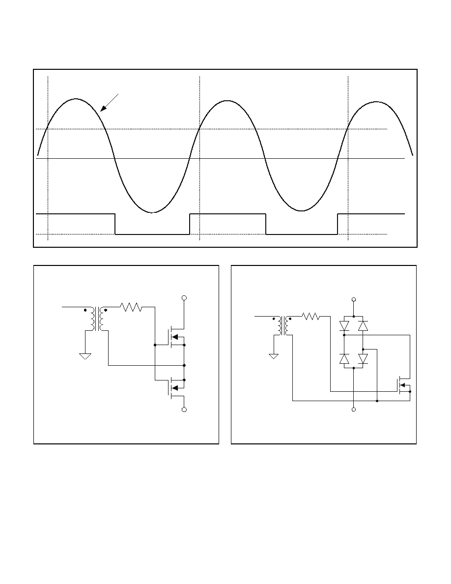
APPLICATION INFORMATION
Power Stage Operation
The power stage used for the UCC3751 application has
two distinct switching circuits which together produce the
required low frequency signal on the output. The primary
side switching circuit consists of a current fed push-pull
resonant circuit that generates the high frequency sinu-
soidal waveform across the transformer winding. The op-
eration of this type of circuit is extensively covered in
Unitrode Application notes U-141 and U-148. Resonant
components C
R1
, C
R2
, L
R
, N should be chosen so that
the
primary
and
secondary
resonances
are
well
matched. Also, for the UCC3751 operation, switching fre-
quency is fixed by crystal selection. So, the resonant
components must be selected to yield a resonant fre-
quency close enough to the switching frequency to get a
low distortion sine-wave. Practically, since it is impossi-
ble to get an exact match between the two frequencies,
the switching frequency should always be higher than
the resonant frequency to ensure low distortion and take
advantage of ZVT operation. Switches Q1 and Q2 are
pulsed at 50% duty cycle at the switching frequency
(89.489 kHz) determined by a crystal (3.579545 MHz)
connected to the UCC3751. The input voltage for the
resonant stage (typically 12V) determines the voltage
stress of Q1 and Q2. Transformer turns ratio is deter-
mined by the output voltage requirements. On the sec-
ondary side, the high frequency waveform is sampled at
a predetermined frequency (e.g. 89.469 kHz) which dif-
fers from the primary switching frequency by the desired
output frequency (e.g. 20 Hz). The sampling is accom-
plished using a bi-directional switching circuit as shown
in Figure 2 and Figure 3. Figure 2 shows the sampling
mechanism consisting of two back-to-back FET switches
allowing current flow in both directions. The sampling
can also be done with a single active switch and a
full-bridge rectifier as shown in Fig. 3. The DRVS pin of
the UCC3751 provides the drive signal for the sampling
switch(es) and this signal is coupled through a pulse
transformer. Typical pulsewidth of the sampling signal is
280ns. As a result of sampling, the resultant output signal
matches the secondary voltage in amplitude and has a
low output frequency desired for ring generation.
The secondary winding of the power transformer also has
a tap (or a separate winding) to generate a loosely regu-
lated DC voltage. This DC voltage can be used to offset
the ring generator output. The UCC3751 is also config-
ured such that the AC output can go to zero under certain
conditions. Table 2 provides the logic levels for different
operating modes of UCC3751. Operation in mode 2 is
achieved by altering the sampling frequency to match the
switching frequency and sampling the secondary AC volt-
age at zero crossings. As a result, the resultant total out-
put voltage between V
OUT
and GND is the semi-regulated
DC voltage achieved through the tapped secondary. This
feature allows the circuit to operate under off-hook and
idle conditions when only the DC portion of the voltage is
required. The activation of this mode occurs when the
OHD voltage exceeds a set threshold or RINGEN is low.
The incorporation of this mode eliminates any need for
external relays or switching circuits as well as eliminating
the need for an additional power supply for powering the
phone. The DC voltage level can be fine tuned by adjust-
ing the voltage on the DELAY pin of the UCC3751. This
pin sets the sampling delay time during the off-hook
mode and allows a DC voltage to be developed between
V
1
and V
OUT
during this mode. Fig. 1 illustrates the oper-
ation of this mode. When the DELAY is set between 0
and 1V, the sampling is done in phase with the primary
switching instances (at points A), leading to an average
voltage of 0V between V
1
and V
OUT
for a sinusoidal sec-
ondary signal. If DELAY is set to another level, the sam-
pling instance shifts
(e.g. to point B) leading to an
effective voltage VB being developed between V
1
and
V
OUT
. The actual V
OUT
is the sum of VB and the DC off-
set voltage derived from the additional (or tapped) wind-
ing (V
1
).
Condition
OHD
RINGEN
Sampling Output Mode
Continuous Ringing
Low
High
Frequency Offset from Primary (Mode 1)
Idle (On Hook, No Ringing)
Low
Low
Synchronized to Primary Frequency with Phase
Controlled by DELAY (Mode 2)
Off-Hook
High
X (Low/High)
Mode 2
Cadenced Ringing
Low
High/Low
Mode 1/Mode 2
Table II. Operating mode selection.
6
UCC2751
UCC3751
UNITRODE CORPORATION
7 CONTINENTAL BLVD. ∑ MERRIMACK, NH 03054
TEL. (603) 424-2410 ∑ FAX (603) 424-3460
TO TRANSFORMER
DRVS
TO OUTPUT
Figure 2. Sampling circuit with two FETs.
TO TRANSFORMER
DRVS
TO OUTPUT
Figure 3. Sampling circuit with single FET and
full-bridge rectifier.
VB
B
0
A
B
A
B
TRANSFORMER SECONDARY
VOLTAGE
0 V
DRV2
Figure 1. Effects of sampling delay during off-hook operation.

IMPORTANT NOTICE
Texas Instruments and its subsidiaries (TI) reserve the right to make changes to their products or to discontinue
any product or service without notice, and advise customers to obtain the latest version of relevant information
to verify, before placing orders, that information being relied on is current and complete. All products are sold
subject to the terms and conditions of sale supplied at the time of order acknowledgment, including those
pertaining to warranty, patent infringement, and limitation of liability.
TI warrants performance of its products to the specifications applicable at the time of sale in accordance with
TI's standard warranty. Testing and other quality control techniques are utilized to the extent TI deems necessary
to support this warranty. Specific testing of all parameters of each device is not necessarily performed, except
those mandated by government requirements.
Customers are responsible for their applications using TI components.
In order to minimize risks associated with the customer's applications, adequate design and operating
safeguards must be provided by the customer to minimize inherent or procedural hazards.
TI assumes no liability for applications assistance or customer product design. TI does not warrant or represent
that any license, either express or implied, is granted under any patent right, copyright, mask work right, or other
intellectual property right of TI covering or relating to any combination, machine, or process in which such
products or services might be or are used. TI's publication of information regarding any third party's products
or services does not constitute TI's approval, license, warranty or endorsement thereof.
Reproduction of information in TI data books or data sheets is permissible only if reproduction is without
alteration and is accompanied by all associated warranties, conditions, limitations and notices. Representation
or reproduction of this information with alteration voids all warranties provided for an associated TI product or
service, is an unfair and deceptive business practice, and TI is not responsible nor liable for any such use.
Resale of TI's products or services with
statements different from or beyond the parameters stated by TI for
that product or service voids all express and any implied warranties for the associated TI product or service,
is an unfair and deceptive business practice, and TI is not responsible nor liable for any such use.
Also see: Standard Terms and Conditions of Sale for Semiconductor Products. www.ti.com/sc/docs/stdterms.htm
Mailing Address:
Texas Instruments
Post Office Box 655303
Dallas, Texas 75265
Copyright
2001, Texas Instruments Incorporated