UCC1800/1/2/3/4/5
UCC2800/1/2/3/4/5
UCC3800/1/2/3/4/5
MARCH 1999 - REVISED SEPTEMBER 2000 - SLUS270A
FEATURES
∑
100
µ
A Typical Starting Supply Current
∑
500
µ
A Typical Operating Supply
Current
∑
Operation to 1MHz
∑
Internal Soft Start
∑
Internal Fault Soft Start
∑
Internal Leading-Edge Blanking of the
Current Sense Signal
∑
1 Amp Totem-Pole Output
∑
70ns Typical Response from
Current-Sense to Gate Drive Output
∑
1.5% Tolerance Voltage Reference
∑
Same Pinout as UC3842 and
UC3842A
DESCRIPTION
The UCC1800/1/2/3/4/5 family of high-speed, low-power integrated cir-
cuits contain all of the control and drive components required for off-line
and DC-to-DC fixed frequency current-mode switching power supplies
with minimal parts count.
These devices have the same pin configuration as the UC1842/3/4/5
family, and also offer the added features of internal full-cycle soft start
and internal leading-edge blanking of the current-sense input.
The UCC1800/1/2/3/4/5 family offers a variety of package options, tem-
perature range options, choice of maximum duty cycle, and choice of crit-
ical voltage levels. Lower reference parts such as the UCC1803 and
UCC1805 fit best into battery operated systems, while the higher refer-
ence and the higher UVLO hysteresis of the UCC1802 and UCC1804
make these ideal choices for use in off-line power supplies.
The UCC180x series is specified for operation from ≠55
o
C to +125
o
C,
the UCC280x series is specified for operation from ≠40
o
C to +85
o
C, and
the UCC380x series is specified for operation from 0
o
C to +70
o
C.
Low-Power BiCMOS Current-Mode PWM
Part Number
Maximum Duty Cycle
Reference Voltage
Turn-On Threshold
Turn-Off Threshold
UCCx800
100%
5V
7.2V
6.9V
UCCx801
50%
5V
9.4V
7.4V
UCCx802
100%
5V
12.5V
8.3V
UCCx803
100%
4V
4.1V
3.6V
UCCx804
50%
5V
12.5V
8.3V
UCCx805
50%
4V
4.1V
3.6V
application
INFO
available
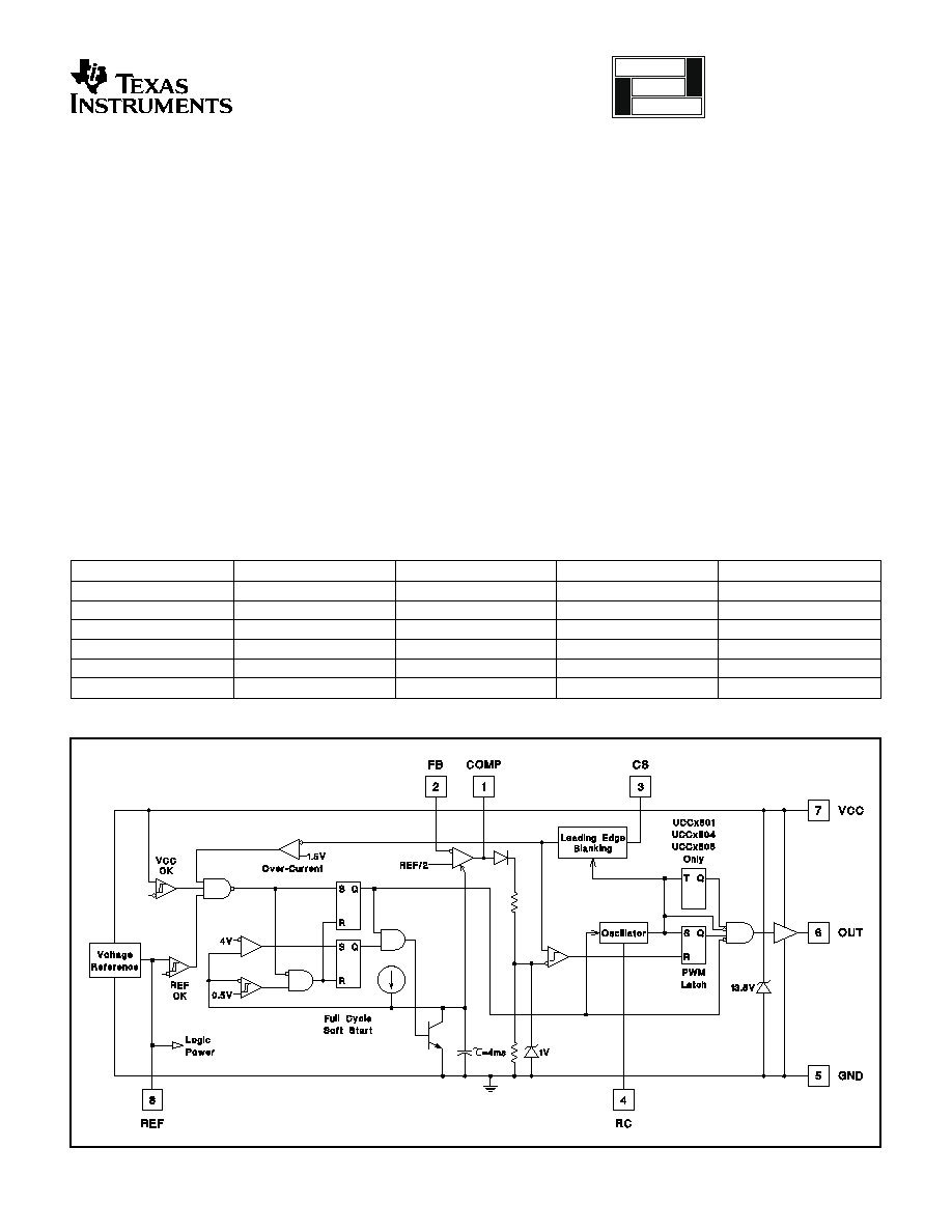
BLOCK DIAGRAM
UDG92009-3
2
UCC1800/1/2/3/4/5
UCC2800/1/2/3/4/5
UCC3800/1/2/3/4/5
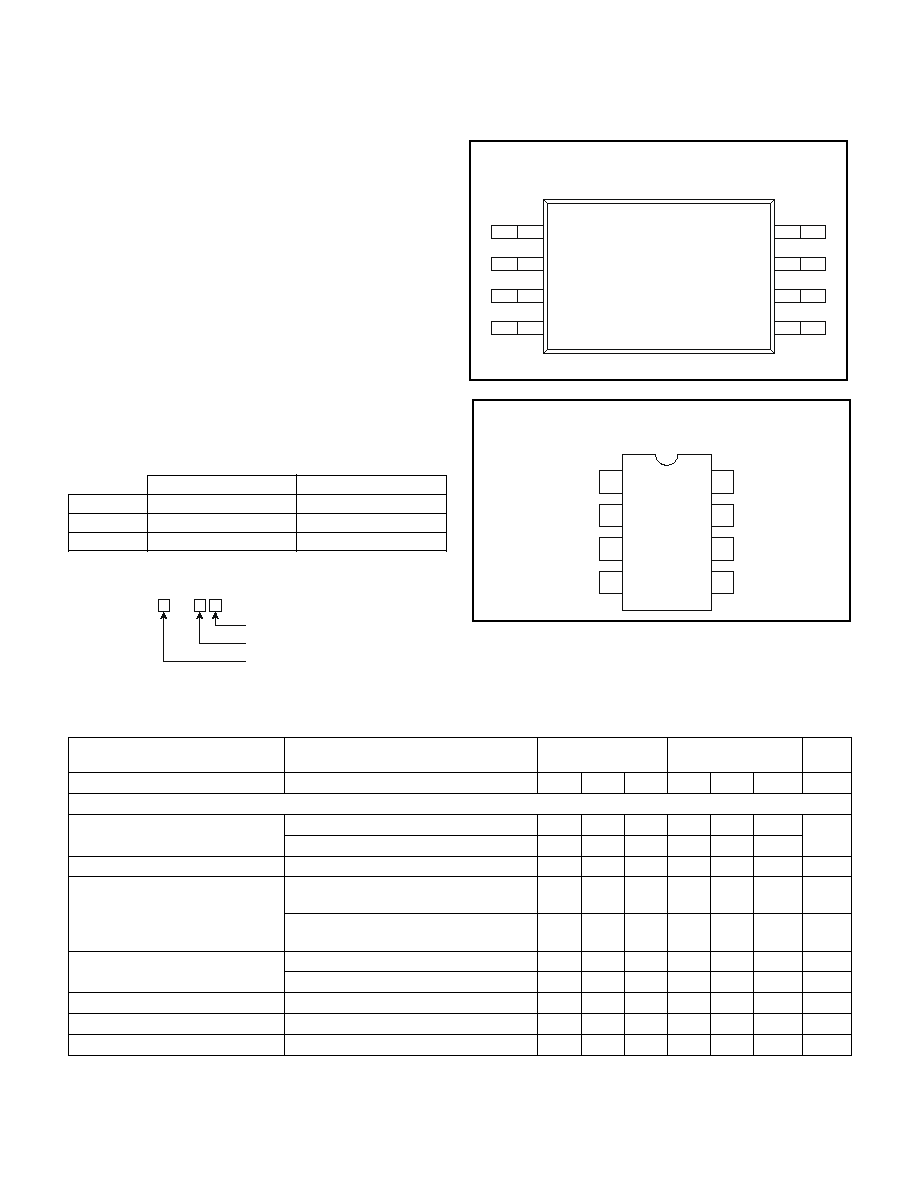
DIL-8, SOIC-8 (Top View)
J or N, D Package
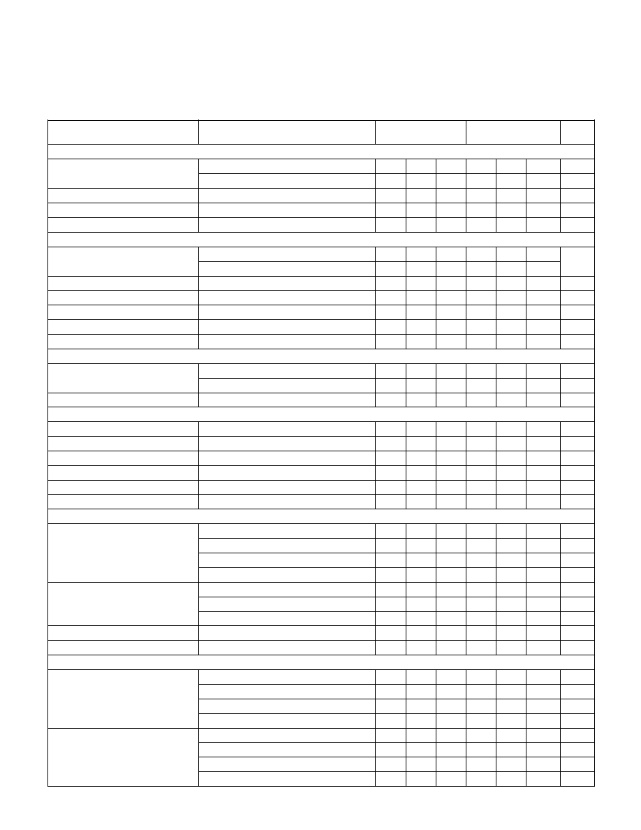
ELECTRICAL CHARACTERISTICS
Unless otherwise stated, these specifications apply for ≠55
∞
C
T
A
+125∞C for
UCC180x; ≠40∞C
T
A
+85∞C for UCC280x; 0∞C
T
A
+70∞C for UCC380x; V
CC
=10V (Note 3); RT=100k from REF to RC;
CT=330pF from RC to GND; 0.1 F capacitor from V
CC
to GND; 0.1 F capacitor from V
REF
to GND. T
A
=T
J
.
PARAMETER
TEST CONDITIONS
UCC180X
UCC280X
UCC380X
UNITS
MIN
TYP
MAX
MIN
TYP
MAX
Reference Section
Output Voltage
T
J
=+25∞C, I=0.2mA, UCCx800/1/2/4
4.925
5.00
5.075 4.925
5.00
5.075
V
T
J
=+25∞C, I=0.2mA, UCCx803/5
3.94
4.00
4.06
3.94
4.00
4.06
Load Regulation
0.2mA<I<5mA
10
30
10
25
mV
Line Regulation
T
J
=+25
∞
C,
V
CC
=10V to Clamp (I
VCC
=25mA)
1.9
1.9
mV/V
T
J
=≠55∞C to +125∞C,
V
CC
=10V to Clamp (I
VCC
=25mA)
2.5
2.1
mV/V
Total Variation
UCCx800/1/2/4 (Note 7)
4.88
5.00
5.10
4.88
5.00
5.10
V
UCCx803/5 (Note 7)
3.90
4.00
4.08
3.90
4.00
4.08
V
Output Noise Voltage
10Hz
f
10kHz, T
J
=+25∞C (Note 9)
130
130
µ
V
Long Term Stability
T
A
=+125∞C, 1000 Hours (Note 9)
5
5
mV
Output Short Circuit
≠5
≠35
≠5
≠35
mA
OUT
VCC
REF
GND
1
2
3
4
8
7
6
5
FB
COMP
CS
RC
ABSOLUTE MAXIMUM RATINGS (Note 1)
V
CC
Voltage (Note 2) . . . . . . . . . . . . . . . . . . . . . . . . . . . . 12.0V
V
CC
Current (Note 2) . . . . . . . . . . . . . . . . . . . . . . . . . . 30.0mA
OUT Current . . . . . . . . . . . . . . . . . . . . . . . . . . . . . . . . . . .
±
1.0A
OUT Energy (Capacitive Load) . . . . . . . . . . . . . . . . . . . 20.0
µ
J
Analog Inputs (FB, CS) . . . . . . . . . . . . . . . . . . . . ≠0.3V to 6.3V
Power Dissipation at T
A
< +25∞C (N or J Package) . . . . . 1.0W
Power Dissipation at T
A
< +25∞C (D Package). . . . . . . . 0.65W
Storage Temperature Range . . . . . . . . . . . . .
≠
65∞C to +150∞C
Lead Temperature (Soldering, 10 Seconds) . . . . . . . . +300∞C
Note 1: Values beyond which damage may occur. All voltages
are with respect to GND. All currents are positive into
the specified terminal. Consult Unitrode databook for
information regarding thermal specifications and limita-
tions of packages.
Note 2: In normal operation V
CC
is powered through a current
limiting resistor. Absolute maximum of 12V applies
when V
CC
is driven from a low impedance source such
that I
CC
does not exceed 30mA (which includes gate
drive current requirement).
COMP
FB
CS
RC
REF
VCC
OUT
GND
8
7
6
5
1
2
3
4
CONNECTION DIAGRAMS
TSSOP-8 (Top View)
PW Package
UCC
PRODUCT OPTION
PACKAGE
80
TEMPERATURE RANGE
ORDERING INFORMATION
Temperature Range
Available Packages
UCC180X
≠55∞C to +125∞C
J
UCC280X
≠40∞C to +85∞C
N, D, PW
UCC380X
0∞C to +70∞C
N, D, PW
TEMPERATURE AND PACKAGE SELECTION
3
UCC1800/1/2/3/4/5
UCC2800/1/2/3/4/5
UCC3800/1/2/3/4/5
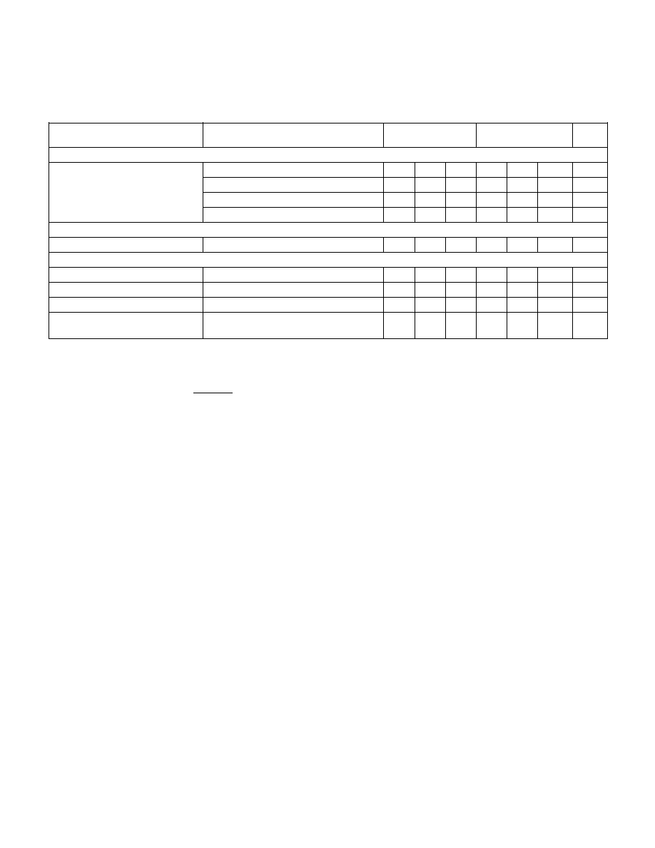
ELECTRICAL CHARACTERISTICS
Unless otherwise stated, these specifications apply for ≠55
∞
C
T
A
+125∞C for
UCC180x; ≠40∞C
T
A
+85∞C for UCC280x; 0∞C
T
A
+70∞C for UCC380x; V
CC
=10V (Note 3); RT=100k from REF to RC;
CT=330pF from RC to GND; 0.1 F capacitor from V
CC
to GND; 0.1 F capacitor from V
REF
to GND. T
A
=T
J
.
PARAMETER
TEST CONDITIONS
UCC180X
UCC280X
UCC380X
UNITS
Oscillator Section
Oscillator Frequency
UCCx800/1/2/4 (Note 4)
40
46
52
40
46
52
kHz
UCCx803/5 (Note 4)
26
31
36
26
31
36
kHz
Temperature Stability
(Note 9)
2.5
2.5
%
Amplitude peak-to-peak
2.25
2.40
2.55
2.25
2.40
2.55
V
Oscillator Peak Voltage
2.45
2.45
V
Error Amplifier Section
Input Voltage
COMP=2.5V; UCCx800/1/2/4
2.44
2.50
2.56
2.44
2.50
2.56
V
COMP=2.0V; UCCx803/5
1.95
2.0
2.05
1.95
2.0
2.05
Input Bias Current
≠
1
1
≠
1
1
µ
A
Open Loop Voltage Gain
60
80
60
80
dB
COMP Sink Current
FB=2.7V, COMP=1.1V
0.3
3.5
0.4
2.5
mA
COMP Source Current
FB=1.8V, COMP=REF≠1.2V
≠0.2
≠0.5
≠0.8
≠0.2
≠0.5
≠0.8
mA
Gain Bandwidth Product
(Note 9)
2
2
MHz
PWM Section
Maximum Duty Cycle
UCCx800/2/3
97
99
100
97
99
100
%
UCCx801/4/5
48
49
50
48
49
50
Minimum Duty Cycle
COMP=0V
0
0
%
Current Sense Section
Gain
(Note 5)
1.10
1.65
1.80
1.10
1.65
1.80
V/V
Maximum Input Signal
COMP=5V (Note 6)
0.9
1.0
1.1
0.9
1.0
1.1
V
Input Bias Current
≠
200
200
≠
200
200
nA
CS Blank Time
50
100
150
50
100
150
ns
Over-Current Threshold
1.42
1.55
1.68
1.42
1.55
1.68
V
COMP to CS Offset
CS=0V
0.45
0.90
1.35
0.45
0.90
1.35
V
Output Section
OUT Low Level
I=20mA, all parts
0.1
0.4
0.1
0.4
V
I=200mA, all parts
0.35
0.90
0.35
0.90
V
I=50mA, VCC=5V, UCCx803/5
0.15
0.40
0.15
0.40
V
I=20mA, VCC=0V, all parts
0.7
1.2
0.7
1.2
V
OUT High V
SAT
(V
CC
-OUT)
I=≠20mA, all parts
0.15
0.40
0.15
0.40
V
I=≠200mA, all parts
1.0
1.9
1.0
1.9
V
I=≠50mA,VCC=5V, UCCx803/5
0.4
0.9
0.4
0.9
V
Rise Time
C
L
=1nF
41
70
41
70
ns
Fall Time
C
L
=1nF
44
75
44
75
ns
Undervoltage Lockout Section
Start Threshold (Note 8)
UCCx800
6.6
7.2
7.8
6.6
7.2
7.8
V
UCCx801
8.6
9.4
10.2
8.6
9.4
10.2
V
UCCx802/4
11.5
12.5
13.5
11.5
12.5
13.5
V
UCCx803/5
3.7
4.1
4.5
3.7
4.1
4.5
V
Stop Threshold (Note 8)
UCCx1800
6.3
6.9
7.5
6.3
6.9
7.5
V
UCCx1801
6.8
7.4
8.0
6.8
7.4
8.0
V
UCCx802/4
7.6
8.3
9.0
7.6
8.3
9.0
V
UCCx803/5
3.2
3.6
4.0
3.2
3.6
4.0
V
4
UCC1800/1/2/3/4/5
UCC2800/1/2/3/4/5
UCC3800/1/2/3/4/5
ELECTRICAL CHARACTERISTICS
Unless otherwise stated, these specifications apply for ≠55
∞
C
T
A
+125∞C for
UCC180x; ≠40∞C
T
A
+85∞C for UCC280x; 0∞C
T
A
+70∞C for UCC380x; V
CC
=10V (Note 3); RT=100k from REF to RC;
CT=330pF from RC to GND; 0.1 F capacitor from V
CC
to GND; 0.1 F capacitor from V
REF
to GND. T
A
=T
J
.
PARAMETER
TEST CONDITIONS
UCC180X
UCC280X
UCC380X
UNITS
Undervoltage Lockout Section (cont.)
Start to Stop Hysteresis
UCCx800
0.12
0.3
0.48
0.12
0.3
0.48
V
UCCx801
1.6
2
2.4
1.6
2
2.4
V
UCCx802/4
3.5
4.2
5.1
3.5
4.2
5.1
V
UCCx803/5
0.2
0.5
0.8
0.2
0.5
0.8
V
Soft Start Section
COMP Rise Time
FB=1.8V, Rise from 0.5V to REF≠1V
4
10
4
10
ms
Overall Section
Start-up Current
V
CC
< Start Threshold
0.1
0.2
0.1
0.2
mA
Operating Supply Current
FB=0V, CS=0V
0.5
1.0
0.5
1.0
mA
VCC Internal Zener Voltage
I
CC
=10mA (Note 8), (Note 10)
12
13.5
15
12
13.5
15
V
VCC Internal Zener Voltage Minus
Start Threshold Voltage
UCCx802/4 (Note 8)
0.5
1.0
0.5
1.0
V
Note 3: Adjust VCC above the start threshold before setting at 10V.
Note 4: Oscillator frequency for the UCCx800, UCCx802 and UCCx803 is the output frequency.
Oscillator frequency for the UCCx801, UCCx804 and UCCx805 is twice the output frequency.
Note 5: Gain is defined by:
A
V
V
V
V
COMP
CS
CS
=
0
0 8
.
.
Note 6: Parameter measured at trip point of latch with Pin 2 at 0V.
Note 7: Total Variation includes temperature stability and load regulation.
Note 8: Start Threshold, Stop Threshold and Zener Shunt Thresholds track one another.
Note 9: Guaranteed by design. Not 100% tested in production.
Note 10: The device is fully operating in clamp mode as the forcing current is higher than the normal operating supply current.
PIN DESCRIPTIONS
COMP: COMP is the output of the error amplifier and the
input of the PWM comparator.
Unlike other devices, the error amplifier in the UCC3800
family is a true, low output-impedance, 2MHz operational
amplifier. As such, the COMP terminal can both source
and sink current. However, the error amplifier is internally
current limited, so that you can command zero duty cycle
by externally forcing COMP to GND.
The UCC3800 family features built-in full cycle Soft Start.
Soft Start is implemented as a clamp on the maximum
COMP voltage.
CS: CS is the input to the current sense comparators.
The UCC3800 family has two different current sense
comparators: the PWM comparator and an over-current
comparator.
The UCC3800 family contains digital current sense filter-
ing, which disconnects the CS terminal from the current
sense comparator during the 100ns interval immediately
following the rising edge of the OUT pin. This digital filter-
ing, also called leading-edge blanking, means that in
most applications, no analog filtering (RC filter) is
required on CS. Compared to an external RC filter tech-
nique, the leading-edge blanking provides a smaller ef-
fective CS to OUT propagation delay. Note, however,
that the minimum non-zero On-Time of the OUT signal is
directly affected by the leading-edge-blanking and the
CS to OUT propagation delay.
The over-current comparator is only intended for fault
sensing, and exceeding the over-current threshold will
cause a soft start cycle.
FB: FB is the inverting input of the error amplifier. For
best stability, keep FB lead length as short as possible
and FB stray capacitance as small as possible.
GND: GND is reference ground and power ground for all
functions on this part.
OUT: OUT is the output of a high-current power driver
capable of driving the gate of a power MOSFET with
peak currents exceeding
±
750mA. OUT is actively held
low when V
CC
is below the UVLO threshold.
5
UCC1800/1/2/3/4/5
UCC2800/1/2/3/4/5
UCC3800/1/2/3/4/5
The high-current power driver consists of FET output de-
vices, which can switch all of the way to GND and all of
the way to V
CC
. The output stage also provides a very
low impedance to overshoot and undershoot. This means
that in many cases, external schottky clamp diodes are
not required.
RC: RC is the oscillator timing pin. For fixed frequency
operation, set timing capacitor charging current by con-
necting a resistor from REF to RC. Set frequency by con-
necting a timing capacitor from RC to GND. For best
performance, keep the timing capacitor lead to GND as
short and direct as possible. If possible, use separate
ground traces for the timing capacitor and all other func-
tions.
The frequency of oscillation can be estimated with the
following equations:
UCCx800/1/2/4:
F
R C
=
∑
1 5
.
UCCx803, UCCx805:
F
R C
=
∑
10
.
where frequency is in Hz, resistance is in ohms, and ca-
pacitance is in farads. The recommended range of timing
resistors is between 10k and 200k and timing capacitor is
100pF to 1000pF. Never use a timing resistor less than
10k.
To prevent noise problems, bypass VCC to GND with a
ceramic capacitor as close to the VCC pin as possible.
An electrolytic capacitor may also be used in addition to
the ceramic capacitor.
REF: REF is the voltage reference for the error amplifier
and also for many other functions on the IC. REF is also
used as the logic power supply for high speed switching
logic on the IC.
When V
CC
is greater than 1V and less than the UVLO
threshold, REF is pulled to ground through a 5k ohm re-
sistor. This means that REF can be used as a logic out-
put indicating power system status. It is important for
reference stability that REF is bypassed to GND with a
ceramic capacitor as close to the pin as possible. An
electrolytic capacitor may also be used in addition to the
ceramic capacitor. A minimum of 0.1
µ
F ceramic is re-
quired. Additional REF bypassing is required for external
loads greater than 2.5mA on the reference.
To prevent noise problems with high speed switching
transients, bypass REF to ground with a ceramic capaci-
tor very close to the IC package.
VCC: V
CC
is the power input connection for this device.
In normal operation V
CC
is powered through a current
limiting resistor. Although quiescent V
CC
current is very
low, total supply current will be higher, depending on
OUT current. Total V
CC
current is the sum of quiescent
V
CC
current and the average OUT current. Knowing the
operating frequency and the MOSFET gate charge (Qg),
average OUT current can be calculated from:
I
Q
F
OUT
g
=
◊
.
PIN DESCRIPTIONS (cont.)
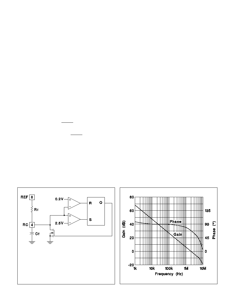
Figure 1. Oscillator.
Figure 2. Error amplifier gain/phase response.
The UCC3800/1/2/3/4/5 oscillator generates a sawtooth
waveform on RC. The rise time is set by the time constant of
R
T
and C
T
. The fall time is set by CT and an internal transis-
tor on-resistance of approximately 125 . During the fall
time, the output is off and the maximum duty cycle is re-
duced below 50% or 100% depending on the part number.
Larger timing capacitors increase the discharge time and re-
duce the maximum duty cycle and frequency.
6
UCC1800/1/2/3/4/5
UCC2800/1/2/3/4/5
UCC3800/1/2/3/4/5
1000
100
10
10
100
1000
Oscillator Freq.
(kHz)
R (k )
T
100pF
200pF
330pF
1nF
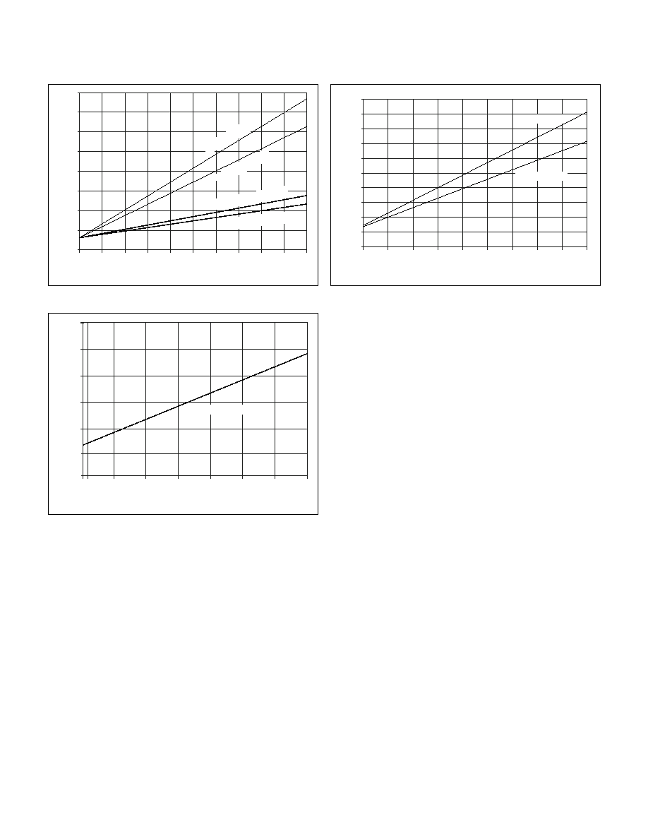
Figure 5. UCC1803/5 oscillator frequency vs. R
T
and
C
T.
95
95.5
96
96.5
97
97.5
98
98.5
99
99.5
100
10
100
1000
Oscillator Frequency (kHz)
Maxim
um Duty Cyc
le (%)
C
=
100pF
T
C
=
200pF
T
C
=
330pF
T
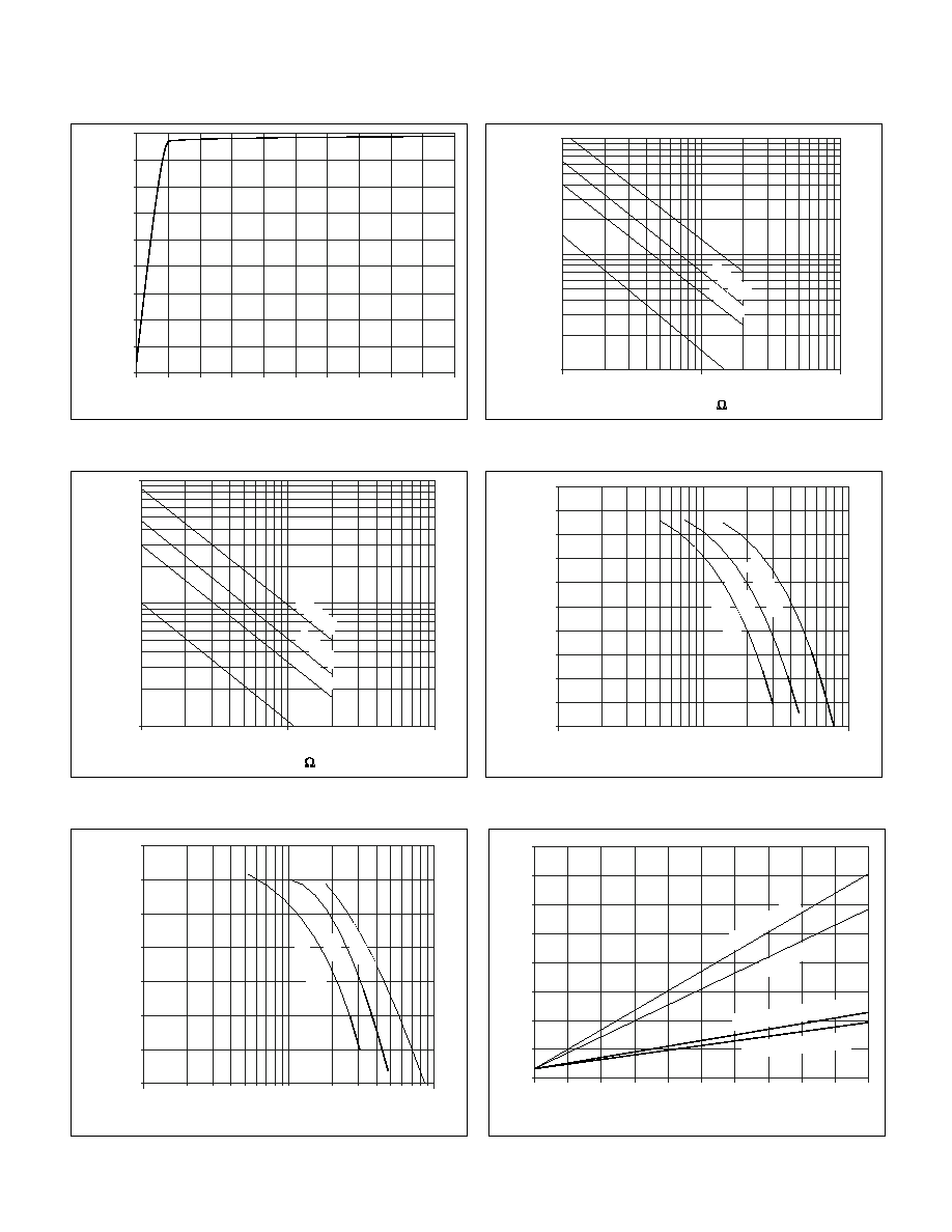
Figure 6. UCC1800/2/3 maximum duty cycle vs.
oscillator frequency.
1000
100
10
10
100
1000
Oscillator Freq.
(kHz)
R (k )
T
100pF
200pF
330pF
1nF
Figure 4. UCC1800/1/2/4 oscillator frequency vs. R
T
and C
T
.
4.00
3.98
3.96
3.94
3.92
3.90
3.88
3.86
3.84
3.82
4
4.2
4.4
4.6
4.8
5
5.2
5.4
5.6
5.8
6
V
(V)
CC
V
(V)
REF
Figure 3. UCC1803/5 V
REF
vs. V
CC
; I
LOAD
= 0.5mA.
46.5
47
47.5
48
48.5
49
49.5
50
10
100
1000
Oscillator Frequency (kHz)
Maxim
um Duty Cyc
le (%)
C
=
100pF
T
C
=
200pF
T
C
=
330pF
T
Figure 7. UCC1801/4/5 maximum duty cycle vs.
oscillator frequency.
0
2
4
6
8
10
12
14
16
0
100
200
300
400
500
600
700
800
900 1000
Oscillator Frequency (kHz)
I
(
mA)
CC
V
= 10V
, 1nF
CC
V = 8V
, 1nF
CC
V = 10V
, No Load
CC
V
= 8V, No Load
CC
Figure 8. UCC1800 I
CC
vs. oscillator frequency.
7
UCC1800/1/2/3/4/5
UCC2800/1/2/3/4/5
UCC3800/1/2/3/4/5
0
50
100
150
200
250
300
350
400
450
500
100
200
300
400
500
600
700
800
900
1000
C
(pF)
T
Dead Tim
e (ns)
UCC1803/5
UCC1800/1/2/4
Figure 9. Dead time vs. C
T
, R
T
= 100k.
0
0.6
0.7
0.8
0.9
1.0
1.1
-55-50
-25
0
25
50
75
100
125
Temperature (∞C)
COMP to CS Offset (V
olts)
Slope = 1.8mV/ C
∞
Figure 10. COMP to CS offset vs. temperature,
CS = 0V.
0
1
2
3
4
5
6
7
8
0
100
200
300
400
500
600
700
800
900 1000
Oscillator Frequency (kHz)
I
(
mA)
CC
V
= 10V
, 1nF
CC
V = 8V
, 1nF
CC
V = 10V
, No Load
CC
V
= 8V, No Load
CC
Figure 8. UCC1805 I
CC
vs. oscillator frequency.
UNITRODE CORPORATION
7 CONTINENTAL BLVD. ∑ MERRIMACK, NH 03054
TEL. (603) 424-2410 ∑ FAX (603) 424-3460

IMPORTANT NOTICE
Texas Instruments and its subsidiaries (TI) reserve the right to make changes to their products or to discontinue
any product or service without notice, and advise customers to obtain the latest version of relevant information
to verify, before placing orders, that information being relied on is current and complete. All products are sold
subject to the terms and conditions of sale supplied at the time of order acknowledgment, including those
pertaining to warranty, patent infringement, and limitation of liability.
TI warrants performance of its products to the specifications applicable at the time of sale in accordance with
TI's standard warranty. Testing and other quality control techniques are utilized to the extent TI deems necessary
to support this warranty. Specific testing of all parameters of each device is not necessarily performed, except
those mandated by government requirements.
Customers are responsible for their applications using TI components.
In order to minimize risks associated with the customer's applications, adequate design and operating
safeguards must be provided by the customer to minimize inherent or procedural hazards.
TI assumes no liability for applications assistance or customer product design. TI does not warrant or represent
that any license, either express or implied, is granted under any patent right, copyright, mask work right, or other
intellectual property right of TI covering or relating to any combination, machine, or process in which such
products or services might be or are used. TI's publication of information regarding any third party's products
or services does not constitute TI's approval, license, warranty or endorsement thereof.
Reproduction of information in TI data books or data sheets is permissible only if reproduction is without
alteration and is accompanied by all associated warranties, conditions, limitations and notices. Representation
or reproduction of this information with alteration voids all warranties provided for an associated TI product or
service, is an unfair and deceptive business practice, and TI is not responsible nor liable for any such use.
Resale of TI's products or services with
statements different from or beyond the parameters stated by TI for
that product or service voids all express and any implied warranties for the associated TI product or service,
is an unfair and deceptive business practice, and TI is not responsible nor liable for any such use.
Also see: Standard Terms and Conditions of Sale for Semiconductor Products. www.ti.com/sc/docs/stdterms.htm
Mailing Address:
Texas Instruments
Post Office Box 655303
Dallas, Texas 75265
Copyright
2001, Texas Instruments Incorporated