 | –≠–ª–µ–∫—Ç—Ä–æ–Ω–Ω—ã–π –∫–æ–º–ø–æ–Ω–µ–Ω—Ç: UCC28050P | –°–∫–∞—á–∞—Ç—å:  PDF PDF  ZIP ZIP |

PRELIMINARY
FLEx18
TM
3.3V 32K/64K/128K/256K/512K x 18
Synchronous Dual-Port RAM
CY7C0837V
CY7C0830V/CY7C0831V
CY7C0832V/CY7C0833V
Cypress Semiconductor Corporation
∑
3901 North First Street
∑
San Jose
,
CA 95134
∑
408-943-2600
Document #: 38-06059 Rev. *K
July 06, 2004
Features
∑ True dual-ported memory cells that allow simultaneous
access of the same memory location
∑ Synchronous pipelined operation
∑ Family of 512-Kbit, 1-Mbit, 2-Mbit, 4-Mbit and 9-Mbit
devices
∑ Pipelined output mode allows fast operation
∑ 0.18-micron CMOS for optimum speed and power
∑ High-speed clock to data access
∑ 3.3V low power
-- Active as low as 225 mA (typ)
-- Standby as low as 55 mA (typ)
∑ Mailbox function for message passing
∑ Global master reset
∑ Separate byte enables on both ports
∑ Commercial and industrial temperature ranges
∑ IEEE 1149.1-compatible JTAG boundary scan
∑ 144-ball FBGA (13 mm ◊ 13 mm) (1.0 mm pitch)
∑ 120TQFP (14 mm x 14 mm x 1.4 mm)
∑ Counter wrap around control
-- Internal mask register controls counter wrap-around
-- Counter-interrupt flags to indicate wrap-around
-- Memory block retransmit operation
∑ Counter readback on address lines
∑ Mask register readback on address lines
∑ Dual Chip Enables on both ports for easy depth
expansion
Functional Description
The FLEx18 family includes 512-Kbit, 1-Mbit, 2-Mbit, 4-Mbit
and 9-Mbit pipelined, synchronous, true dual-port static RAMs
that are high-speed, low-power 3.3V CMOS. Two ports are
provided, permitting independent, simultaneous access to any
location in memory. The result of writing to the same location
by more than one port at the same time is undefined. Registers
on control, address, and data lines allow for minimal set-up
and hold time.
During a Read operation, data is registered for decreased
cycle time. Each port contains a burst counter on the input
address register. After externally loading the counter with the
initial address, the counter will increment the address inter-
nally (more details to follow). The internal Write pulse width is
independent of the duration of the R/W input signal. The
internal Write pulse is self-timed to allow the shortest possible
cycle times.
A HIGH on CE0 or LOW on CE1 for one clock cycle will power
down the internal circuitry to reduce the static power
consumption. One cycle with chip enables asserted is required
to reactivate the outputs.
Additional features include: readback of burst-counter internal
address value on address lines, counter-mask registers to
control the counter wrap-around, counter interrupt (CNTINT)
flags, readback of mask register value on address lines,
retransmit functionality, interrupt flags for message passing,
JTAG for boundary scan, and asynchronous Master Reset
(MRST).
The CY7C0833V device in this family has limited features.
Please see Address Counter and Mask Register
Operations
[15]
on page 6 for details.
Table 1. Product Selection Guide
Density
512-Kbit
(32K x 18)
1-Mbit
(64K x 18)
2-Mbit
(128K x 18)
4-Mbit
(256K x 18)
9-Mbit
(512K x 18)
Part Number
CY7C0837V
CY7C0830V
CY7C0831V
CY7C0832V
CY7C0833V
Max. Speed (MHz)
167
167
167
167
133
Max. Access Time - clock to Data (ns)
4.0
4.0
4.0
4.0
4.7
Typical operating current (mA)
225
225
225
225
270
Package
144 FBGA
120 TQFP
144 FBGA
120 TQFP
144 FBGA
120 TQFP
144 FBGA
144 FBGA
CY7C093794V CY7C093894V CY7C09289V CY7C09369V CY7C09379V CY7C09389V3.3V 64K/128K x 36 and 128K/256K x 18
Synchronous Dual-Port RAM
PRELIMINARY
CY7C0837V
CY7C0830V/CY7C0831V
CY7C0832V/CY7C0833V
Document #: 38-06059 Rev. *K
Page 2 of 28
Note:
1.
CY7C0837V has 15 address CY7C0830V has 16 address bits, CY7C0831V has 17 address bits, CY7C0832V has 18 address bits and CY7C0833V has 19
address bits
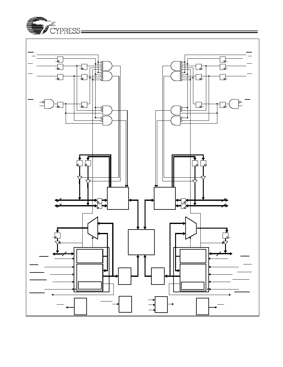
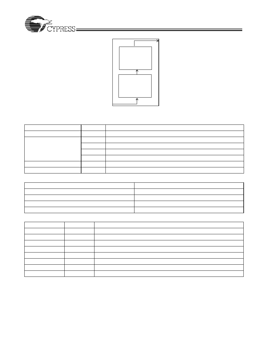
Logic Block Diagram
[1]
DQ
9R
≠DQ
17R
DQ
0R
≠DQ
8R
A
0L
≠A
18L
CLK
L
ADS
L
CNTEN
L
CNTRST
L
True
RAM Array
19
Addr.
Read
Back
CNTINT
L
Mask Register
Counter/
Address
Register
CNT/MSK
L
Address
Decode
Dual-Ported
Interrupt
Logic
INT
L
Reset
Logic
JTAG
TDO
TMS
TCK
TDI
MRST
DQ
9L
≠DQ
17L
DQ
0L
≠DQ
8L
I/O
Control
9
9
CE
0L
CE
1L
R/W
L
B0
L
B1
L
OE
L
A
0R
≠A
18R
CLK
R
ADS
CNTEN
CNTRST
R
19
Addr.
Read
Back
CNTINT
R
Mask Register
Counter/
Address
Register
CNT/MSK
R
Address
Decode
Interrupt
Logic
INT
R
I/O
Control
9
9
CE
0R
CE
1R
R/W
R
B0
R
B1
R
OE
R
Mirror Reg
Mirror Reg

PRELIMINARY
CY7C0837V
CY7C0830V/CY7C0831V
CY7C0832V/CY7C0833V
Document #: 38-06059 Rev. *K
Page 3 of 28
Pin Configurations
144-ball BGA
Top View
CY7C0837V / CY7C0830V / CY7C0831V
CY7C0832V / CY7C0833V
1
2
3
4
5
6
7
8
9
10
11
12
A
DQ17
L
DQ16
L
DQ14
L
DQ12
L
DQ10
L
DQ9
L
DQ9
R
DQ10
R
DQ12
R
DQ14
R
DQ16
R
DQ17
R
B
A0
L
A1
L
DQ15
L
DQ13
L
DQ11
L
MRST
NC
DQ11
R
DQ13
R
DQ15
R
A1
R
A0
R
C
A2
L
A3
L
CE1
L
[6]
INT
L
CNTINT
L
[8]
ADS
L
[7]
ADS
R
[7]
CNTINT
R
[8]
INT
R
CE1
R
[6]
A3
R
A2
R
D
A4
L
A5
L
CE0
L
[7]
NC
VDDIO
L
VDDIO
L
VDDIO
R
VDDIO
R
NC
CE0
R
[7]
A5
R
A4
R
E
A6
L
A7
L
B1
L
NC
VDDIO
L
VSS
VSS
VDDIO
R
NC
B1
R
A7
R
A6
R
F
A8
L
A9
L
C
L
NC
VSS
VSS
VSS
VSS
NC
C
R
A9
R
A8
R
G
A10
L
A11
L
B0
L
NC
VSS
VSS
VSS
VSS
NC
B0
R
A11
R
A10
R
H
A12
L
A13
L
OE
L
NC
VDDIO
L
VSS
VSS
VDDIO
R
NC
OE
R
A13
R
A12
R
J
A14
L
A15
L
[2]
RW
L
NC
VDDIO
L
VDDIO
L
VDDIO
R
VDDIO
R
NC
RW
R
A15
R
[2]
A14
R
K
A16
L
[3]
A17
L
[4]
CNT/MSK
L
[6]
TDO
CNTRST
L
[6]
TCK
TMS
CNTRST
R
[6]
TDI
CNT/MSK
R
[6]
A17
R
[4]
A16
R
[3]
L
A18
L
[5]
NC
DQ6
L
DQ4
L
DQ2
L
CNTEN
L
[7]
CNTEN
R
[7]
DQ2
R
DQ4
R
DQ6
R
NC
A18
R
[5]
M
DQ8
L
DQ7
L
DQ5
L
DQ3
L
DQ1
L
DQ0
L
DQ0
R
DQ1
R
DQ3
R
DQ5
R
DQ7
R
DQ8
R
Notes:
2.
Leave this ball unconnected for CY7C0837V
3.
Leave this ball unconnected for CY7C0837V and CY7C0830V
4.
Leave this ball unconnected for CY7C0837V, CY7C0830V and CY7C0831V
5.
Leave this ball unconnected for CY7C0837V, CY7C0830V, CY7C0831V and CY7C0832V
6.
These balls are not applicable for CY7C0833V device. They need to be tied to VDDIO.
7.
These balls are not applicable for CY7C0833V device. They need to be tied to VSS.
8.
These balls are not applicable for CY7C0833V device. They need to be no connected.

PRELIMINARY
CY7C0837V
CY7C0830V/CY7C0831V
CY7C0832V/CY7C0833V
Document #: 38-06059 Rev. *K
Page 4 of 28
Pin Configurations (continued)
12
0
11
9
11
8
11
7
11
6
11
5
11
4
11
3
11
2
11
1
11
0
10
9
10
8
10
7
10
6
10
5
10
4
10
3
10
2
10
1
10
0
99
98
97
96
95
94
93
92
91
DQ
11
L
CNT
I
N
T
L
INT
L
DQ
9L
DQ
10
L
DQ
12
L
V
SS
V
DD
DQ
13
L
DQ
14
L
DQ
15
L
DQ
16
L
DQ
17
L
A
0L
A
1L
DQ
16
R
A
1R
A
0R
DQ
17
R
DQ
15
R
DQ
14
R
DQ
13
R
V
DD
V
SS
DQ
12
R
DQ
11
R
DQ
10
R
DQ
9R
INT
R
CNT
I
N
T
R
90
89
88
87
86
85
84
83
82
81
80
79
78
77
76
75
74
73
72
71
70
69
68
67
66
65
64
63
62
61
B
1R
V
SS
V
DD
CE
0R
OE
R
B
0R
CE
1R
A
7R
A
6R
A
5R
A
4R
V
DD
V
SS
A
3R
A
2R
A
12R
A
13R
V
DD
V
SS
A
11R
A
10R
A
9R
A
8R
CNT/MSK
R
CNTRST
R
CNTEN
R
ADS
R
MRST
CLK
R
R/W
R
31
32
33
34
35
36
37
38
39
40
41
42
43
44
45
46
47
48
49
50
51
52
53
54
55
56
57
58
59
60
V
SS
DQ
0L
DQ
1L
DQ
2L
DQ
3L
V
DD
DQ
4L
DQ
5L
DQ
6L
DQ
7L
DQ
8L
A
17
L
[10
]
A
16
L
[9]
A
15
L
A
14
L
A
17
R
[10
]
A
14
R
A
15
R
A
16
R
[9]
DQ
8R
DQ
7R
DQ
6R
DQ
5R
DQ
4R
V
DD
V
SS
DQ
3R
DQ
2R
DQ
1R
DQ
0R
1
2
3
4
5
6
7
8
9
10
11
12
13
14
15
16
17
18
19
20
21
22
23
24
25
26
27
28
29
30
B
1L
V
SS
V
DD
CE
0L
OE
L
B
0L
A
7L
A
6L
A
5L
A
4L
V
DD
V
SS
A
3L
A
2L
A
12L
A
13L
V
DD
V
SS
A
11L
A
10L
A
9L
A
8L
CNT/MSK
L
CNTRST
L
CNTEN
L
ADS
L
V
SS
CLK
L
R/W
L
CE
1L
120-pin Thin Quad Flat Pack (TQFP)
Top View
CY7C0830V / CY7C0831V / CY7C0832V
Notes:
9.
Leave this pin unconnected for CY7C0830V
10. Leave this pin unconnected for CY7C0830V and CY7C0831V
PRELIMINARY
CY7C0837V
CY7C0830V/CY7C0831V
CY7C0832V/CY7C0833V
Document #: 38-06059 Rev. *K
Page 5 of 28
Pin Definitions
Left Port
Right Port
Description
A
0L
≠A
18L
[1]
A
0R
≠A
18R
[1]
Address Inputs.
ADS
L
[7]
ADS
R
[7]
Address Strobe Input. Used as an address qualifier. This signal should be asserted LOW
for the part using the externally supplied address on the address pins and for loading this
address into the burst address counter.
CE0
L
[7]
CE0
R
[7]
Active LOW Chip Enable Input.
CE1
L
[6]
CE1
R
[6]
Active HIGH Chip Enable Input.
CLK
L
CLK
R
Clock Signal. Maximum clock input rate is f
MAX
.
CNTEN
L
[7]
CNTEN
R
[7]]
Counter Enable Input. Asserting this signal LOW increments the burst address counter of
its respective port on each rising edge of CLK. The increment is disabled if ADS or CNTRST
are asserted LOW.
CNTRST
L
[6]
CNTRST
R
[6]
Counter Reset Input. Asserting this signal LOW resets to zero the unmasked portion of
the burst address counter of its respective port. CNTRST is not disabled by asserting ADS
or CNTEN.
CNT/MSK
L
[6]
CNT/MSK
R
[6]
Address Counter Mask Register Enable Input. Asserting this signal LOW enables access
to the mask register. When tied HIGH, the mask register is not accessible and the address
counter operations are enabled based on the status of the counter control signals.
DQ
0L
≠DQ
17L
[1]
DQ
0R
≠DQ
17R
[1]
Data Bus Input/Output.
OE
L
OE
R
Output Enable Input. This asynchronous signal must be asserted LOW to enable the DQ
data pins during Read operations.
INT
L
INT
R
Mailbox Interrupt Flag Output. The mailbox permits communications between ports. The
upper two memory locations can be used for message passing. INT
L
is asserted LOW when
the right port writes to the mailbox location of the left port, and vice versa. An interrupt to a
port is deasserted HIGH when it reads the contents of its mailbox.
CNTINT
L
[8]
CNTINT
R
[8]
Counter Interrupt Output. This pin is asserted LOW when the unmasked portion of the
counter is incremented to all "1s."
R/W
L
R/W
R
Read/Write Enable Input. Assert this pin LOW to write to, or HIGH to Read from the dual
port memory array.
B
0L
≠B
3L
B
0R
≠B
1R
Byte Select Inputs. Asserting these signals enables Read and Write operations to the
corresponding bytes of the memory array.
MRST
Master Reset Input. MRST is an asynchronous input signal and affects both ports.
Asserting MRST LOW performs all of the reset functions as described in the text. A MRST
operation is required at power-up.
TMS
JTAG Test Mode Select Input. It controls the advance of JTAG TAP state machine. State
machine transitions occur on the rising edge of TCK.
TDI
JTAG Test Data Input. Data on the TDI input will be shifted serially into selected registers.
TCK
JTAG Test Clock Input.
TDO
JTAG Test Data Output. TDO transitions occur on the falling edge of TCK. TDO is normally
three-stated except when captured data is shifted out of the JTAG TAP.
V
SS
Ground Inputs.
V
DD
Power Inputs.

PRELIMINARY
CY7C0837V
CY7C0830V/CY7C0831V
CY7C0832V/CY7C0833V
Document #: 38-06059 Rev. *K
Page 6 of 28
Master Reset
The FLEx18 family devices undergo a complete reset by
taking its MRST input LOW. The MRST input can switch
asynchronously to the clocks. An MRST initializes the internal
burst counters to zero, and the counter mask registers to all
ones (completely unmasked). MRST also forces the Mailbox
Interrupt (INT) flags and the Counter Interrupt (CNTINT) flags
HIGH. MRST must be performed on the FLEx18 family
devices after power-up.
Mailbox Interrupts
The upper two memory locations may be used for message
passing and permit communications between ports. Table 2
shows the interrupt operation for both ports of CY7C0833V.
The highest memory location, 7FFFF is the mailbox for the
right port and 7FFFE is the mailbox for the left port. Table 2
shows that in order to set the INT
R
flag, a Write operation by
the left port to address 7FFFF will assert INT
R
LOW. At least
one byte has to be active for a Write to generate an interrupt.
A valid Read of the 7FFFF location by the right port will reset
INT
R
HIGH. At least one byte has to be active in order for a
Read to reset the interrupt. When one port Writes to the other
port's mailbox, the INT of the port that the mailbox belongs to
is asserted LOW. The INT is reset when the owner (port) of the
mailbox Reads the contents of the mailbox. The interrupt flag
is set in a flow-thru mode (i.e., it follows the clock edge of the
writing port). Also, the flag is reset in a flow-thru mode (i.e., it
follows the clock edge of the reading port).
Each port can read the other port's mailbox without resetting
the interrupt. And each port can write to its own mailbox
without setting the interrupt. If an application does not require
message passing, INT pins should be left open.
Address Counter and Mask Register Operations
[15]
This section describes the features only apply to
512Kbit,1Mbit, 2Mbit, and 4Mbit devices. It does not apply to
9Mbit device. Each port of these devices has a programmable
burst address counter. The burst counter contains three
registers: a counter register, a mask register, and a mirror
register.
The counter register contains the address used to access the
RAM array. It is changed only by the Counter Load, Increment,
Counter Reset, and by master reset (MRST) operations.
The mask register value affects the Increment and Counter
Reset operations by preventing the corresponding bits of the
counter register from changing. It also affects the counter
interrupt output (CNTINT). The mask register is changed only
by the Mask Load and Mask Reset operations, and by the
MRST. The mask register defines the counting range of the
counter register. It divides the counter register into two
regions: zero or more "0s" in the most significant bits define
the masked region, one or more "1s" in the least significant bits
define the unmasked region. Bit 0 may also be "0," masking
the least significant counter bit and causing the counter to
increment by two instead of one.
The mirror register is used to reload the counter register on
increment operations (see "retransmit," below). It always
contains the value last loaded into the counter register, and is
changed only by the Counter Load, and Counter Reset opera-
tions, and by the MRST. Table 3 summarizes the operation of
these registers and the required input control signals. The
MRST control signal is asynchronous. All the other control
signals in Table 3 (CNT/MSK, CNTRST, ADS, CNTEN) are
synchronized to the port's CLK. All these counter and mask
operations are independent of the port's chip enable inputs
(CE0 and CE1).
Counter enable (CNTEN) inputs are provided to stall the
operation of the address input and utilize the internal address
generated by the internal counter for fast, interleaved memory
applications. A port's burst counter is loaded when the port's
address strobe (ADS) and CNTEN signals are LOW. When the
port's CNTEN is asserted and the ADS is deasserted, the
address counter will increment on each LOW to HIGH
transition of that port's clock signal. This will Read/Write one
word from/into each successive address location until CNTEN
s deasserted. The counter can address the entire memory
array, and will loop back to the start. Counter reset (CNTRST)
is used to reset the unmasked portion of the burst counter to
i0s. A counter-mask register is used to control the counter
wrap.
Table 2. Interrupt Operation Example
[1,11,12,13,14,16]
FUNCTION
LEFT PORT
RIGHT PORT
R/W
L
CE
L
A
0L
-
A
18L
INT
L
R/W
R
CE
R
A
0R
-
A
18R
INT
R
Set Right INT
R
Flag
L
L
3FFFF
X
X
X
X
L
Reset Right INT
R
Flag
X
X
X
X
H
L
3FFFF
H
Set Left INT
L
Flag
X
X
X
L
L
L
3FFFE
X
Reset Left INT
L
Flag
H
L
3FFFE
H
X
X
X
X
Set Right INT
R
Flag
L
L
3FFFF
X
X
X
X
L
Notes:
11. CE is internal signal. CE = LOW if CE
0
= LOW and CE
1
= HIGH. For a single Read operation, CE only needs to be asserted once at the rising edge of the
CLK and can be deasserted after that. Data will be out after the following CLK edge and will be three-stated after the next CLK edge.
12. OE is "Don't Care" for mailbox operation.
13. At least one of BE0, BE1 must be LOW.
14. A18x is a NC for CY7C0832V, therefore the Interrupt Addresses are 3FFFF and 3FFFE. A18x and A17x are NC for CY7C0831V, therefore the Interrupt
addresses are 1FFFF and 1FFFE; A18x, A17x and A16x are NC for CY7C0830V, therefore the Interrupt Addresses are FFFF and FFFE;A18x, A17x, A16x
and A15x are NC for CY7C0837V, therefore the Interrupt Addresses are 7FFF and 7FFE.
15. This section describes the CY7C0832V, CY7C0831V, CY7C0830V and CY7C0837V having 18, 17, 16 and 15 address bits.
16. "X" = "Don't Care," "H" = HIGH, "L" = LOW.

PRELIMINARY
CY7C0837V
CY7C0830V/CY7C0831V
CY7C0832V/CY7C0833V
Document #: 38-06059 Rev. *K
Page 7 of 28
Counter Reset Operation
All unmasked bits of the counter and mirror registers are reset
to "0." All masked bits remain unchanged. A Mask Reset
followed by a Counter Reset will reset the counter and mirror
registers to 00000, as will master reset (MRST).
Counter Load Operation
The address counter and mirror registers are both loaded with
the address value presented at the address lines.
Counter Increment Operation
Once the address counter register is initially loaded with an
external address, the counter can internally increment the
address value, potentially addressing the entire memory array.
Only the unmasked bits of the counter register are incre-
mented. The corresponding bit in the mask register must be
a "1" for a counter bit to change. The counter register is incre-
mented by 1 if the least significant bit is unmasked, and by 2
if it is masked. If all unmasked bits are "1," the next increment
will wrap the counter back to the initially loaded value. If an
Increment results in all the unmasked bits of the counter being
"1s," a counter interrupt flag (CNTINT) is asserted. The next
Increment will return the counter register to its initial value,
which was stored in the mirror register. The counter address
can instead be forced to loop to 00000 by externally
connecting CNTINT to CNTRST.
[18]
An increment that results
in one or more of the unmasked bits of the counter being "0"
will de-assert the counter interrupt flag. The example in
Figure 2
shows the counter mask register loaded with a mask
value of 0003Fh unmasking the first 6 bits with bit "0" as the
LSB and bit "16" as the MSB. The maximum value the mask
register can be loaded with is 3FFFFh. Setting the mask
register to this value allows the counter to access the entire
memory space. The address counter is then loaded with an
initial value of 8h. The base address bits (in this case, the 6th
address through the 16th address) are loaded with an address
value but do not increment once the counter is configured for
increment operation. The counter address will start at address
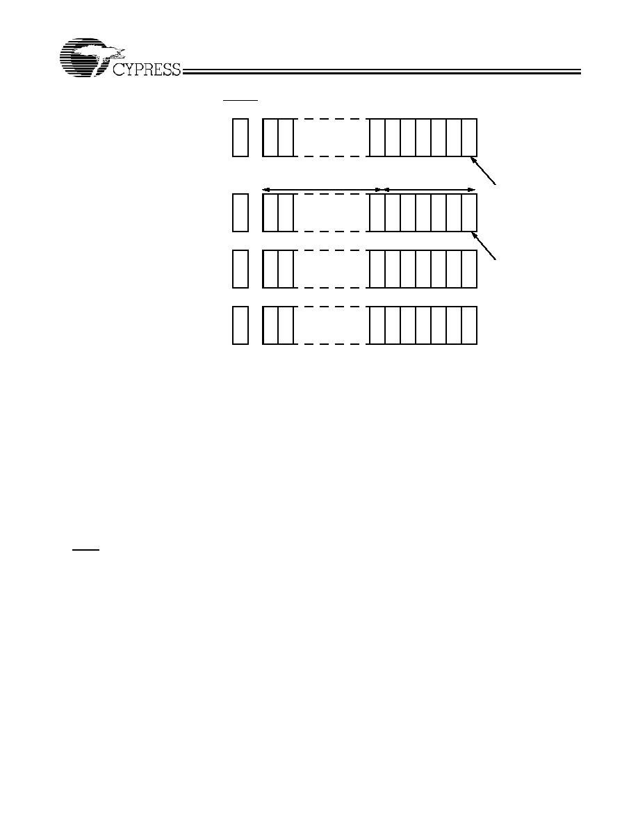
8h. The counter will increment its internal address value till it
reaches the mask register value of 3Fh. The counter wraps
around the memory block to location 8h at the next count.
CNTINT is issued when the counter reaches its maximum
value
Counter Hold Operation
The value of all three registers can be constantly maintained
unchanged for an unlimited number of clock cycles. Such
operation is useful in applications where wait states are
needed, or when address is available a few cycles ahead of
data in a shared bus interface.
Counter Interrupt
The counter interrupt (CNTINT) is asserted LOW when an
increment operation results in the unmasked portion of the
counter register being all "1s." It is deasserted HIGH when an
Increment operation results in any other value. It is also
de-asserted by Counter Reset, Counter Load, Mask Reset
and Mask Load operations, and by MRST.
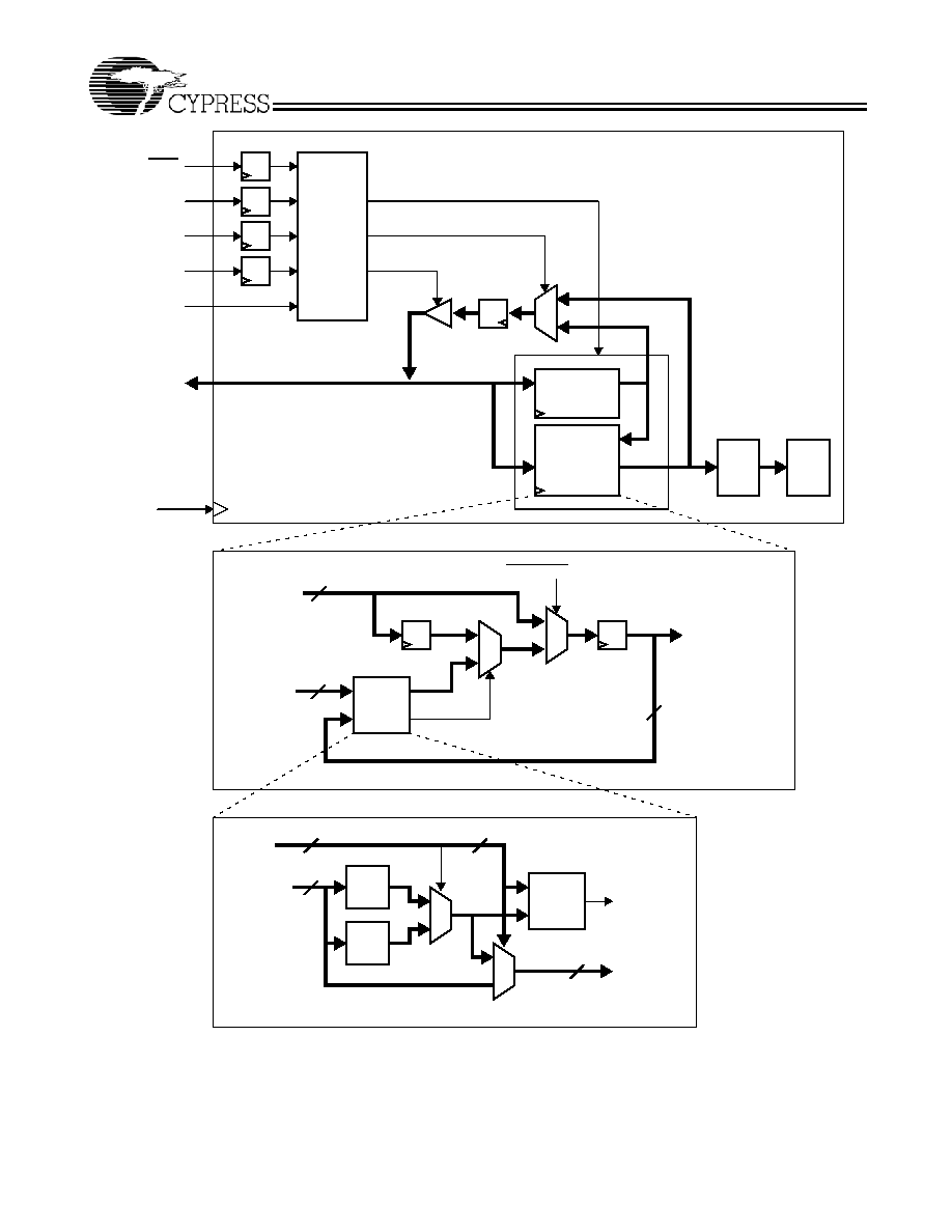
Counter Readback Operation
The internal value of the counter register can be read out on
the address lines. Readback is pipelined; the address will be
valid t
CA2
after the next rising edge of the port's clock. If
address readback occurs while the port is enabled (CE0 LOW
and CE1 HIGH), the data lines (DQs) will be three-stated.
Figure 1 shows a block diagram of the operation.
.
Table 3. Address Counter and Counter-Mask Register Control Operation (Any Port)
[16, 17]
CLK
MRST CNT/MSK
CNTRST
ADS
CNTEN
Operation
Description
X
L
X
X
X
X
Master Reset
Reset address counter to all 0s and mask
register to all 1s.
H
H
L
X
X
Counter Reset
Reset counter unmasked portion to all 0s.
H
H
H
L
L
Counter Load
Load counter with external address value
presented on address lines.
H
H
H
L
H
Counter
Readback
Read out counter internal value on address
lines.
H
H
H
H
L
Counter Increment Internally increment address counter value.
H
H
H
H
H
Counter Hold
Constantly hold the address value for
multiple clock cycles.
H
L
L
X
X
Mask Reset
Reset mask register to all 1s.
H
L
H
L
L
Mask Load
Load mask register with value presented on
the address lines.
H
L
H
L
H
Mask Readback
Read out mask register value on address
lines.
H
L
H
H
X
Reserved
Operation undefined
Notes:
17. Counter operation and mask register operation is independent of chip enables.
18. CNTINT and CNTRST specs are guaranteed by design to operate properly at speed grade operating frequency when tied together.

PRELIMINARY
CY7C0837V
CY7C0830V/CY7C0831V
CY7C0832V/CY7C0833V
Document #: 38-06059 Rev. *K
Page 8 of 28
Retransmit
Retransmit is a feature that allows the Read of a block of
memory more than once without the need to reload the initial
address. This eliminates the need for external logic to store
and route data. It also reduces the complexity of the system
design and saves board space. An internal "mirror register" is
used to store the initially loaded address counter value. When
the counter unmasked portion reaches its maximum value set
by the mask register, it wraps back to the initial value stored in
this "mirror register." If the counter is continuously configured
in increment mode, it increments again to its maximum value
and wraps back to the value initially stored into the "mirror
register." Thus, the repeated access of the same data is
allowed without the need for any external logic.
Mask Reset Operation
The mask register is reset to all "1s," which unmasks every bit
of the counter. Master reset (MRST) also resets the mask
register to all "1s."
Mask Load Operation
The mask register is loaded with the address value presented
at the address lines. Not all values permit correct increment
operations. Permitted values are of the form 2
n
≠ 1 or 2
n
≠ 2.
From the most significant bit to the least significant bit,
permitted values have zero or more "0s," one or more "1s," or
one "0." Thus 3FFFF, 003FE, and 00001 are permitted values,
but 3F0FF, 003FC, and 00000 are not.
Mask Readback Operation
The internal value of the mask register can be read out on the
address lines. Readback is pipelined; the address will be valid
t
CM2
after the next rising edge of the port's clock. If mask
readback occurs while the port is enabled (CE0 LOW and CE1
HIGH), the data lines (DQs) will be three-stated. Figure 1
shows a block diagram of the operation.
Counting by Two
When the least significant bit of the mask register is "0," the
counter increments by two. This may be used to connect the
x18 devices as a 36-bit single port SRAM in which the counter
of one port counts even addresses and the counter of the other
port counts odd addresses. This even-odd address scheme
stores one half of the 36-bit data in even memory locations,
and the other half in odd memory locations.
PRELIMINARY
CY7C0837V
CY7C0830V/CY7C0831V
CY7C0832V/CY7C0833V
Document #: 38-06059 Rev. *K
Page 9 of 28
From
Mask
Register
Mirror
Counter
Address
Decode
RAM
Array
Wrap
1
0
Increment
Logic
1
0
+1
+2
1
0
Wrap
Detect
From
Mask
From
Counter
To
Counter
Bit 0
Wrap
Figure 1. Counter, Mask, and Mirror Logic Block Diagram
[1]
17
17
17
17
17
1
0
Load/Increment
CNT/MSK
CNTEN
ADS
CNTRST
CLK
Decode
Logic
Bidirectional
Address
Lines
Mask
Register
Counter/
Address
Register
From
Address
Lines
To Readback
and Address
Decode
17
17
MRST
PRELIMINARY
CY7C0837V
CY7C0830V/CY7C0831V
CY7C0832V/CY7C0833V
Document #: 38-06059 Rev. *K
Page 10 of 28
IEEE 1149.1 Serial Boundary Scan (JTAG)
[20]
The FLEx18 family devices incorporate an IEEE 1149.1 serial
boundary scan test access port (TAP). The TAP controller
functions in a manner that does not conflict with the operation
of other devices using 1149.1-compliant TAPs. The TAP
operates using JEDEC-standard 3.3V I/O logic levels. It is
composed of three input connections and one output
connection required by the test logic defined by the standard.
Performing a TAP Reset
A reset is performed by forcing TMS HIGH (V
DD
) for five rising
edges of TCK. This reset does not affect the operation of the
devices, and may be performed while the device is operating.
An MRST must be performed on the devices after power-up.
Performing a Pause/Restart
When a SHIFT-DR PAUSE-DR SHIFT-DR is performed the
scan chain will output the next bit in the chain twice. For
example, if the value expected from the chain is 1010101, the
device will output a 11010101. This extra bit will cause some
testers to report an erroneous failure for the devices in a scan
test. Therefore the tester should be configured to never enter
the PAUSE-DR state.
Boundary Scan Hierarchy for 9-Mbit Device
Internally, the CY7C0833V have two DIEs. Each DIE contain
all the circuitry required to support boundary scan testing. The
circuitry includes the TAP, TAP controller, instruction register,
and data registers. The circuity and operation of the DIE
boundary scan are described in detail below. The scan chain
of each DIE are connected serially to form the scan chain of
the CY7C0833V as shown in Figure 3. TMS and TCK are
connected in parallel to each DIE to drive all TAP controllers
in unison. In many cases, each DIE will be supplied with the
same instruction. In other cases, it might be useful to supply
different instructions to each DIE. One example would be
testing the device ID of one DIE while bypassing the others.
Each pin of FLEx18 family is typically connected to multiple
DIEs. For connectivity testing with the EXTEST instruction, it
is desirable to check the internal connections between DIEs
as well as the external connections to the package. This can
be accomplished by merging the netlist of the devices with the
netlist of the user's circuit board. To facilitate boundary scan
testing of the devices, Cypress provides the BSDL file for each
DIE, the internal netlist of the device, and a description of the
device scan chain. The user can use these materials to easily
integrate the devices into the board's boundary scan
environment. Further information can be found in the Cypress
application note Using JTAG Boundary Scan For System in a
Package (SIP) Dual-Port SRAMs.
2
16
2
15
2
6
2
1
2
5
2
2
2
4
2
3
2
0
2
16
2
15
2
6
2
1
2
5
2
2
2
4
2
3
2
0
2
16
2
15
2
6
2
1
2
5
2
2
2
4
2
3
2
0
2
16
2
15
2
6
2
1
2
5
2
2
2
4
2
3
2
0
H
H
L
H
1 1
0s
1
0
1
0
1
0
1
0 0
Xs
1
X
0
X
0
X
0
1 1
Xs
1
X
1
X
1
X
1
0 0
Xs
1
X
0
X
0
X
0
Masked Address
Unmasked Address
Mask
Register
bit-0
Address
Counter
bit-0
CNTINT
Example:
Load
Counter-Mask
Register = 3F
Load
Address
Counter = 8
Max
Address
Register
Max + 1
Address
Register
Figure 2. Programmable Counter-Mask Register Operation
[1, 19]
Notes:
19. The "X" in this diagram represents the counter upper bits
20. Boundary scan is IEEE 1149.1-compatible. See "Performing a Pause/Restart" for deviation from strict 1149.1 compliance
PRELIMINARY
CY7C0837V
CY7C0830V/CY7C0831V
CY7C0832V/CY7C0833V
Document #: 38-06059 Rev. *K
Page 11 of 28
Table 4. Identification Register Definitions
Instruction Field
Value
Description
Revision Number (31:28)
0h
Reserved for version number.
Cypress Device ID
(27:12)
C090h
Defines Cypress part number for CY7C0832V
C091h
Defines Cypress part number for CY7C0831V
C093h
Defines Cypress part number for CY7C0830V
C094h
Defines Cypress part number for CY7C0837V.
Cypress JEDEC ID (11:1)
034h
Allows unique identification of the DP family device vendor.
ID Register Presence (0)
1
Indicates the presence of an ID register.
Table 5. Scan Registers Sizes
Register Name
Bit Size
Instruction
4
Bypass
1
Identification
32
Boundary Scan
n
[21]
Table 6. Instruction Identification Codes
Instruction
Code
Description
EXTEST
0000
Captures the Input/Output ring contents. Places the BSR between the TDI and TDO.
BYPASS
1111
Places the BYR between TDI and TDO.
IDCODE
1011
Loads the IDR with the vendor ID code and places the register between TDI and TDO.
HIGHZ
0111
Places BYR between TDI and TDO. Forces all device output drivers to a High-Z state.
CLAMP
0100
Controls boundary to 1/0. Places BYR between TDI and TDO.
SAMPLE/PRELOAD 1000
Captures the input/output ring contents. Places BSR between TDI and TDO.
NBSRST
1100
Resets the non-boundary scan logic. Places BYR between TDI and TDO.
RESERVED
All other codes Other combinations are reserved. Do not use other than the above.
Notes:
21. See details in the device BSDL file.
D2
TDO
TDI
D1
TDO
TDI
TDI
TDO
Figure 3. Scan Chain for 9Mb Device
PRELIMINARY
CY7C0837V
CY7C0830V/CY7C0831V
CY7C0832V/CY7C0833V
Document #: 38-06059 Rev. *K
Page 12 of 28
Maximum Ratings
[22]
(Above which the useful life may be impaired. For user guide-
lines, not tested.)
Storage Temperature ................................. ≠65
∞
C to +150
∞
C
Ambient Temperature with
Power Applied.............................................≠55
∞
C to +125
∞
C
Supply Voltage to Ground Potential ............... ≠0.5V to +4.6V
DC Voltage Applied to
Outputs in High-Z State...........................≠0.5V to V
DD
+0.5V
DC Input Voltage .............................. ≠0.5V to V
DD
+ 0.5V
[23]
Output Current into Outputs (LOW)............................. 20 mA
Static Discharge Voltage........................................... > 2000V
(JEDEC JESD22-A114-2000B)
Latch-up Current..................................................... > 200 mA
Operating Range
Range
Ambient
Temperature
V
DD
Commercial
0
∞
C to +70
∞
C 3.3V±165
mV
Industrial
≠40
∞
C to +85
∞
C 3.3V±165
mV
Electrical Characteristics
Over the Operating Range
Parameter
Description
-167
-133
-100
Unit
Min. Typ. Max. Min. Typ. Max. Min. Typ. Max.
V
OH
Output HIGH Voltage
(V
DD
= Min., I
OH
= ≠4.0 mA)
2.4
2.4
2.4
V
V
OL
Output LOW Voltage
(V
DD
= Min., I
OL
= +4.0 mA)
0.4
0.4
0.4
V
V
IH
Input HIGH Voltage
2.0
2.0
2.0
V
V
IL
Input LOW Voltage
0.8
0.8
0.8
V
I
OZ
Output Leakage Current
≠10
10
≠10
10
≠10
10
mA
I
IX1
Input Leakage Current Except TDI, TMS, MRST
≠10
10
≠10
10
≠10
10
mA
I
IX2
Input Leakage Current TDI, TMS, MRST
≠0.1
1.0 ≠0.1
1.0
≠0.1
1.0
mA
I
CC
Operating Current for
(V
DD
= Max.,I
OUT
= 0 mA), Outputs
Disabled
CY7C0837V
CY7C0830V
CY7C0831V
CY7C0832V
225 300
225
300
mA
CY7C0833V
270
400
200
310
mA
I
SB1
[24]
Standby Current
(Both Ports TTL Level)
CE
L
and CE
R
S V
IH
, f = f
MAX
90
115
90
115
90
115
mA
I
SB2
[24]
Standby Current
(One Port TTL Level)
CE
L
| CE
R
S V
IH
, f = f
MAX
160 210
160
210
160
210
mA
I
SB3
[24]
Standby Current
(Both Ports CMOS Level)
CE
L
and CE
R
S V
DD
≠ 0.2V, f = 0
55
75
55
75
55
75
mA
I
SB4
[24]
Standby Current
(One Port CMOS Level)
CE
L
| CE
R
S V
IH
, f = f
MAX
160 210
160
210
160
210
mA
Capacitance
[25]
Part Number
Parameter
Description
Test Conditions
Max.
Unit
CY7C0837V
CY7C0830V
CY7C0831V
CY7C0832V
C
IN
Input Capacitance
T
A
= 25
∞
C, f = 1 MHz,
V
DD
= 3.3V
13
pF
C
OUT
Output Capacitance
10
pF
CY7C0833V
C
IN
Input Capacitance
22
pF
C
OUT
Output Capacitance
20
pF
Note:
22. The voltage on any input or I/O pin can not exceed the power pin during power-up.
23. Pulse width < 20 ns.
24. I
SB1
, I
SB2
, I
SB3
and I
SB4
are not applicable for CY7C0833V because it can not be powered down by using chip enable pins.
25. C
OUT
also references C
I/O

PRELIMINARY
CY7C0837V
CY7C0830V/CY7C0831V
CY7C0832V/CY7C0833V
Document #: 38-06059 Rev. *K
Page 13 of 28
AC Test Load and Waveforms
R1 = 590
R2 = 435
C = 5 pF
(b) Three-state Delay (Load 2)
90%
10%
3.0V
Vss
90%
10%
< 2 ns
< 2 ns
ALL INPUT PULSES
3.3V
V
TH
= 1.5V
R = 50
Z
0
= 50
(a) Normal Load (Load 1)
C = 10 pF
OUTPUT
OUTPUT
Switching Characteristics Over the Operating Range
Parameter
Description
-167
-133
-100
Unit
CY7C0837V
CY7C0830V
CY7C0831V
CY7C0832V
CY7C0837V
CY7C0830V
CY7C0831V
CY7C0832V
CY7C0833V
CY7C0833V
Min.
Max.
Min.
Max.
Min.
Max.
Min.
Max.
f
MAX2
Maximum Operating Frequency
167
133
133
100
MHz
t
CYC2
Clock Cycle Time
6.0
7.5
7.5
10
ns
t
CH2
Clock HIGH Time
2.7
3.0
3.0
4.0
ns
t
CL2
Clock LOW Time
2.7
3.0
3.0
4.0
ns
t
R
[26]
Clock Rise Time
2.0
2.0
2.0
3.0
ns
t
F
[26]
Clock Fall Time
2.0
2.0
2.0
3.0
ns
t
SA
Address Set-up Time
2.3
2.5
2.5
3.0
ns
t
HA
Address Hold Time
0.6
0.6
0.6
0.6
ns
t
SB
Byte Select Set-up Time
2.3
2.5
2.5
3.0
ns
t
HB
Byte Select Hold Time
0.6
0.6
0.6
0.6
ns
t
SC
Chip Enable Set-up Time
2.3
2.5
NA
NA
ns
t
HC
Chip Enable Hold Time
0.6
0.6
NA
NA
ns
t
SW
R/W Set-up Time
2.3
2.5
2.5
3.0
ns
t
HW
R/W Hold Time
0.6
0.6
0.6
0.6
ns
t
SD
Input Data Set-up Time
2.3
2.5
2.5
3.0
ns
t
HD
Input Data Hold Time
0.6
0.6
0.6
0.6
ns
t
SAD
ADS Set-up Time
2.3
2.5
NA
NA
ns
t
HAD
ADS Hold Time
0.6
0.6
NA
NA
ns
t
SCN
CNTEN Set-up Time
2.3
2.5
NA
NA
ns
t
HCN
CNTEN Hold Time
0.6
0.6
NA
NA
ns
t
SRST
CNTRST Set-up Time
2.3
2.5
NA
NA
ns
Notes:
26. Except JTAG signals (t
r
and t
f
< 10 ns [max.]).
27. This parameter is guaranteed by design, but it is not production tested.
28. Test conditions used are Load 2.

PRELIMINARY
CY7C0837V
CY7C0830V/CY7C0831V
CY7C0832V/CY7C0833V
Document #: 38-06059 Rev. *K
Page 14 of 28
t
HRST
CNTRST Hold Time
0.6
0.6
NA
NA
ns
t
SCM
CNT/MSK Set-up Time
2.3
2.5
NA
NA
ns
t
HCM
CNT/MSK Hold Time
0.6
0.6
NA
NA
ns
t
OE
Output Enable to Data Valid
4.0
4.4
4.7
5.0
ns
t
OLZ
[27,28]
OE to Low Z
0
0
ns
t
OHZ
[27,28]
OE to High Z
0
4.0
0
4.4
4.7
5.0
ns
t
CD2
Clock to Data Valid
4.0
4.4
4.7
5.0
ns
t
CA2
Clock to Counter Address Valid
4.0
4.4
NA
NA
ns
t
CM2
Clock to Mask Register Readback
Valid
4.0
4.4
NA
NA
ns
t
DC
Data Output Hold After Clock HIGH
1.0
1.0
1.0
1.0
ns
t
CKHZ
[27,28]
Clock HIGH to Output High Z
0
4.0
0
4.4
4.7
5.0
ns
t
CKLZ
[27, 28]
Clock HIGH to Output Low Z
1.0
4.0
1.0
4.4
1.0
4.7
1.0
5.0
ns
t
SINT
Clock to INT Set Time
0.5
6.7
0.5
7.5
0.5
7.5
0.5
10
ns
t
RINT
Clock to INT Reset Time
0.5
6.7
0.5
7.5
0.5
7.5
0.5
10
ns
t
SCINT
Clock to CNTINT Set Time
0.5
5.0
0.5
5.7
NA
NA
NA
NA
ns
t
RCINT
Clock to CNTINT Reset time
0.5
5.0
0.5
5.7
NA
NA
NA
NA
ns
Port to Port Delays
t
CCS
Clock to Clock Skew
5.2
6.0
6.0
8.0
ns
Master Reset Timing
t
RS
Master Reset Pulse Width
7.0
7.5
7.5
10
ns
t
RS
Master Reset Set-up Time
6.0
6.0
6.0
8.5
ns
t
RSR
Master Reset Recovery Time
6.0
7.5
7.5
10
ns
t
RSF
Master Reset to Outputs Inactive
6.0
6.5
6.5
8.0
ns
t
RSCNTINT
Master Reset to Counter Interrupt
Flag Reset Time
5.8
7.0
NA
NA
ns
Switching Characteristics Over the Operating Range
(continued)
Parameter
Description
-167
-133
-100
Unit
CY7C0837V
CY7C0830V
CY7C0831V
CY7C0832V
CY7C0837V
CY7C0830V
CY7C0831V
CY7C0832V
CY7C0833V
CY7C0833V
Min.
Max.
Min.
Max.
Min.
Max.
Min.
Max.

PRELIMINARY
CY7C0837V
CY7C0830V/CY7C0831V
CY7C0832V/CY7C0833V
Document #: 38-06059 Rev. *K
Page 15 of 28
JTAG Timing and Switching Waveforms
Parameter
Description
CY7C0837V/CY7C0830V
CY7C0831V/CY7C0832V
CY7C0833V
Unit
Min.
Max.
f
JTAG
Maximum JTAG TAP Controller Frequency
10
MHz
t
TCYC
TCK Clock Cycle Time
100
ns
t
TH
TCK Clock HIGH Time
40
ns
t
TL
TCK Clock LOW Time
40
ns
t
TMSS
TMS Set-up to TCK Clock Rise
10
ns
t
TMSH
TMS Hold After TCK Clock Rise
10
ns
t
TDIS
TDI Set-up to TCK Clock Rise
10
ns
t
TDIH
TDI Hold After TCK Clock Rise
10
ns
t
TDOV
TCK Clock LOW to TDO Valid
30
ns
t
TDOX
TCK Clock LOW to TDO Invalid
0
ns
Test Clock
Test Mode Select
TCK
TMS
Test Data-In
TDI
Test Data-Out
TDO
t
TCYC
t
TMSH
t
TL
t
TH
t
TMSS
t
TDIS
t
TDIH
t
TDOX
t
TDOV

PRELIMINARY
CY7C0837V
CY7C0830V/CY7C0831V
CY7C0832V/CY7C0833V
Document #: 38-06059 Rev. *K
Page 16 of 28
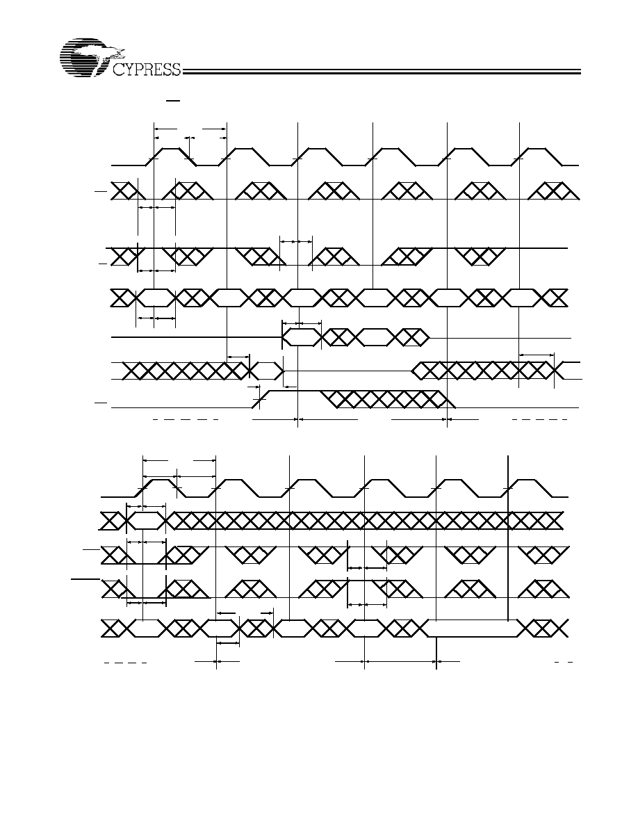
Switching Waveforms
Master Reset
Read Cycle
[11, 29, 30, 31, 32]
Notes:
29. OE is asynchronously controlled; all other inputs (excluding MRST and JTAG) are synchronous to the rising clock edge.
30. ADS = CNTEN = LOW, and MRST = CNTRST = CNT/MSK = HIGH.
31. The output is disabled (high-impedance state) by CE = V
IH
following the next rising edge of the clock.
32. Addresses do not have to be accessed sequentially since ADS = CNTEN = V
IL
with CNT/MSK = V
IH
constantly loads the address on the rising edge of the CLK.
Numbers are for reference only.
MRST
t
RSR
t
RS
INACTIVE
ACTIVE
TMS
TDO
INT
CNTINT
t
RSF
t
RSS
ALL
ADDRESS/
DATA
LINES
ALL
OTHER
INPUTS
t
CH2
t
CL2
t
CYC2
t
SC
t
HC
t
SW
t
HW
t
SA
t
HA
A
n
A
n+1
CLK
CE
R/W
ADDRESS
DATA
OUT
OE
A
n+2
A
n+3
t
SC
t
HC
t
OHZ
t
OE
t
OLZ
t
DC
t
CD2
t
CKLZ
Q
n
Q
n+1
Q
n+2
1 Latency
BE0≠BE1
t
SB
t
HB

PRELIMINARY
CY7C0837V
CY7C0830V/CY7C0831V
CY7C0832V/CY7C0833V
Document #: 38-06059 Rev. *K
Page 17 of 28
Bank Select Read
[33, 34]
Read-to-Write-to-Read (OE = LOW)
[32, 35, 36, 37, 38]
Notes:
33. In this depth-expansion example, B1 represents Bank #1 and B2 is Bank #2; each bank consists of one Cypress FLEx18 device from this data sheet. ADDRESS
(B1)
= ADDRESS
(B2)
.
34. ADS = CNTEN= BE0 ≠ BE1 = OE = LOW; MRST = CNTRST = CNT/MSK = HIGH.
35. Output state (HIGH, LOW, or high-impedance) is determined by the previous cycle control signals.
36. During "No Operation," data in memory at the selected address may be corrupted and should be rewritten to ensure data integrity.
37.
CE
0
= OE = BE0 ≠ BE1 = LOW; CE
1
= R/W = CNTRST = MRST = HIGH.
38. CE
0
= BE0 ≠ BE1 = R/W = LOW; CE
1
= CNTRST = MRST = CNT/MSK = HIGH. When R/W first switches low, since OE = LOW, the Write operation cannot be
completed (labelled as no operation). One clock cycle is required to three-state the I/O for the Write operation on the next rising edge of CLK.
Switching Waveforms
(continued)
Q
3
Q
1
Q
0
Q
2
A
0
A
1
A
2
A
3
A
4
A
5
Q
4
A
0
A
1
A
2
A
3
A
4
A
5
t
SA
t
HA
t
SC
t
HC
t
SA
t
HA
t
SC
t
HC
t
SC
t
HC
t
SC
t
HC
t
CKHZ
t
DC
t
DC
t
CD2
t
CKLZ
t
CD2
t
CD2
t
CKHZ
t
CKLZ
t
CD2
t
CKHZ
t
CKLZ
t
CD2
t
CH2
t
CL2
t
CYC2
CLK
ADDRESS
(B1)
CE
(B1)
DATA
OUT(B2)
DATA
OUT(B1)
ADDRESS
(B2)
CE
(B2)
t
CYC2
t
CL2
t
CH2
t
HC
t
SC
t
HW
t
SW
t
HA
t
SA
t
HW
t
SW
t
CD2
t
CKHZ
t
SD
t
HD
t
CKLZ
t
CD2
NO
OPERATION
WRITE
READ
READ
CLK
CE
R/W
ADDRESS
DATA
IN
DATA
OUT
A
n
A
n+1
A
n+2
A
n+2
D
n+2
A
n+3
A
n+4
Q
n
Q
n+3
PRELIMINARY
CY7C0837V
CY7C0830V/CY7C0831V
CY7C0832V/CY7C0833V
Document #: 38-06059 Rev. *K
Page 18 of 28
Read-to-Write-to-Read (OE Controlled)
[32, 35, 37, 38]
Read with Address Counter Advance
[37]
Switching Waveforms
(continued)
t
CYC2
t
CL2
t
CH2
t
HC
t
SC
t
HW
t
SW
t
HA
t
SA
A
n
A
n+1
A
n+2
A
n+3
A
n+4
A
n+5
t
HW
t
SW
t
SD
t
HD
D
n+2
t
CD2
t
OHZ
READ
READ
WRITE
D
n+3
Q
n
CLK
CE
R/W
ADDRESS
DATA
IN
DATA
OUT
OE
Q
n+4
t
CD2
t
SA
t
HA
t
CH2
t
CL2
t
CYC2
CLK
ADDRESS
A
n
COUNTER HOLD
READ WITH COUNTER
t
SAD
t
HAD
t
SCN
t
HCN
t
SAD
t
HAD
t
SCN
t
HCN
Q
x≠1
Q
x
Q
n
Q
n+1
Q
n+2
Q
n+3
t
DC
t
CD2
READ WITH COUNTER
READ
EXTERNAL
ADDRESS
ADS
CNTEN
DATA
OUT
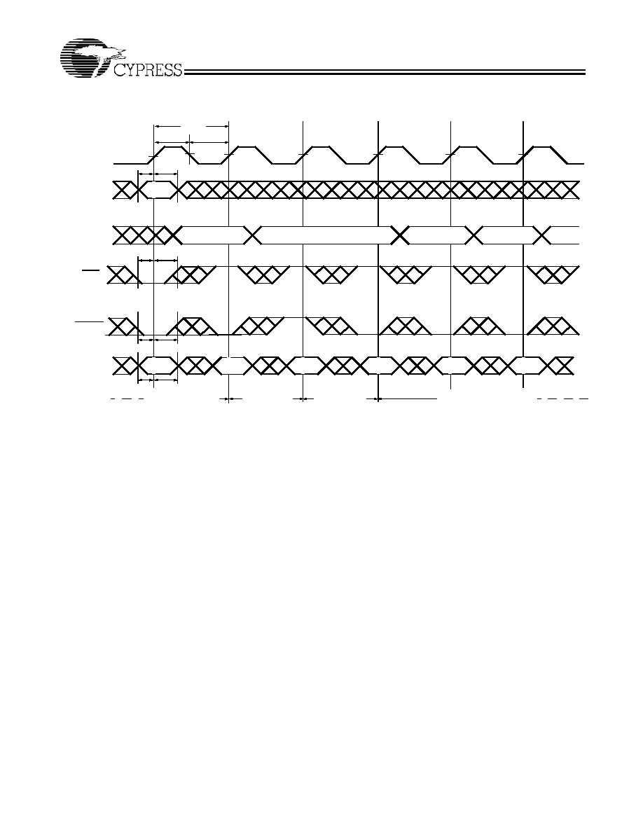
PRELIMINARY
CY7C0837V
CY7C0830V/CY7C0831V
CY7C0832V/CY7C0833V
Document #: 38-06059 Rev. *K
Page 19 of 28
Write with Address Counter Advance
[38]
Switching Waveforms
(continued)
t
CH2
t
CL2
t
CYC2
A
n
A
n+1
A
n+2
A
n+3
A
n+4
D
n+1
D
n+1
D
n+2
D
n+3
D
n+4
A
n
D
n
t
SAD
t
HAD
t
SCN
t
HCN
t
SD
t
HD
WRITE EXTERNAL
WRITE WITH COUNTER
ADDRESS
WRITE WITH
COUNTER
WRITE COUNTER
HOLD
CLK
ADDRESS
INTERNAL
DATA
IN
ADDRESS
t
SA
t
HA
CNTEN
ADS

PRELIMINARY
CY7C0837V
CY7C0830V/CY7C0831V
CY7C0832V/CY7C0833V
Document #: 38-06059 Rev. *K
Page 20 of 28
Counter Reset
[39, 40]
Notes:
39. CE
0
= BE0 ≠ BE1 = LOW; CE
1
= MRST = CNT/MSK = HIGH.
40. No dead cycle exists during counter reset. A Read or Write cycle may be coincidental with the counter reset.
Switching Waveforms
(continued)
CLK
ADDRESS
INTERNAL
CNTEN
ADS
DATA
IN
ADDRESS
CNTRST
R/W
DATA
OUT
A
n
A
m
A
p
A
x
0
1
A
n
A
m
A
p
Q
1
Q
n
Q
0
D
0
t
CH2
t
CL2
t
CYC2
t
SA
t
HA
t
SW
t
HW
t
SRST
t
HRST
t
SD
t
HD
t
CD2
t
CD2
t
CKLZ
[52]
RESET
ADDRESS 0
COUNTER
WRITE
READ
ADDRESS 0
ADDRESS 1
READ
READ
ADDRESS A
n
ADDRESS A
m
READ

PRELIMINARY
CY7C0837V
CY7C0830V/CY7C0831V
CY7C0832V/CY7C0833V
Document #: 38-06059 Rev. *K
Page 21 of 28
Readback State of Address Counter or Mask Register
[41, 42, 43, 44]
Notes:
41. CE
0
= OE = BE0 ≠ BE1 = LOW; CE
1
= R/W = CNTRST = MRST = HIGH.
42. Address in output mode. Host must not be driving address bus after t
CKLZ
in next clock cycle.
43. Address in input mode. Host can drive address bus after t
CKHZ
.
44. An * is the internal value of the address counter (or the mask register depending on the CNT/MSK level) being Read out on the address lines.
Switching Waveforms
(continued)
CNTEN
CLK
t
CH2
t
CL2
t
CYC2
ADDRESS
ADS
A
n
Q
x-2
Q
x-1
Q
n
t
SA
t
HA
t
SAD
t
HAD
t
SCN
t
HCN
LOAD
ADDRESS
EXTERNAL
t
CD2
INTERNAL
ADDRESS
A
n+1
A
n+2
A
n
t
CKHZ
DATA
OUT
A
n*
Q
n+3
Q
n+1
Q
n+2
A
n+3
A
n+4
t
CKLZ
t
CA2
or t
CM2
READBACK
INTERNAL
COUNTER
ADDRESS
INCREMENT
EXTERNAL
A
0
≠A
16
PRELIMINARY
CY7C0837V
CY7C0830V/CY7C0831V
CY7C0832V/CY7C0833V
Document #: 38-06059 Rev. *K
Page 22 of 28
Left_Port (L_Port) Write to Right_Port (R_Port) Read
[45, 46, 47]
Notes:
45. CE
0
= OE = ADS = CNTEN = BE0 ≠ BE1 = LOW; CE
1
= CNTRST = MRST = CNT/MSK = HIGH.
46. This timing is valid when one port is writing, and other port is reading the same location at the same time. If t
CCS
is violated, indeterminate data will be Read out.
47. If t
CCS
< minimum specified value, then R_Port will Read the most recent data (written by L_Port) only (2 * t
CYC2
+ t
CD2
) after the rising edge of R_Port's clock.
If t
CCS
> minimum specified value, then R_Port will Read the most recent data (written by L_Port) (t
CYC2
+ t
CD2
) after the rising edge of R_Port's clock.
Switching Waveforms
(continued)
t
SA
t
HA
t
SW
t
HW
t
CH2
t
CL2
t
CYC2
CLK
L
R/W
L
A
n
D
n
t
CKHZ
t
HD
t
SA
A
n
t
HA
Q
n
t
DC
t
CCS
t
SD
t
CKLZ
t
CH2
t
CL2
t
CYC2
t
CD2
L_PORT
ADDRESS
L_PORT
DATA
IN
CLK
R
R/W
R
R_PORT
ADDRESS
R_PORT
DATA
OUT

PRELIMINARY
CY7C0837V
CY7C0830V/CY7C0831V
CY7C0832V/CY7C0833V
Document #: 38-06059 Rev. *K
Page 23 of 28
Counter Interrupt and Retransmit
[14, 48, 49, 50, 51, 52]
Notes:
48. CE
0
= OE = BE0 ≠ BE1 = LOW; CE
1
= R/W = CNTRST = MRST = HIGH.
49. CNTINT is always driven.
50. CNTINT goes LOW when the unmasked portion of the address counter is incremented to the maximum value.
51. The mask register assumed to have the value of 3FFFFh.
52. Retransmit happens if the counter remains in increment mode after it wraps to initially loaded value.
Switching Waveforms
(continued)
t
CH2
t
CL2
t
CYC2
CLK
3FFFD
3FFFF
INTERNAL
ADDRESS
Last_Loaded
Last_Loaded +1
t
HCM
COUNTER
3FFFE
CNTINT
t
SCINT
t
RCINT
3FFFC
CNTEN
ADS
CNT/MSK
t
SCM

PRELIMINARY
CY7C0837V
CY7C0830V/CY7C0831V
CY7C0832V/CY7C0833V
Document #: 38-06059 Rev. *K
Page 24 of 28
MailBox Interrupt Timing
[53, 54, 55, 56, 57]
Table 7. Read/Write and Enable Operation
(Any Port)
[1, 16, 58, 59, 60]
Inputs
Outputs
Operation
OE
CLK
CE
0
CE
1
R/W
DQ
0
≠ DQ
17
X
H
X
X
High-Z
Deselected
X
X
L
X
High-Z
Deselected
X
L
H
L
D
IN
Write
L
L
H
H
D
OUT
Read
H
X
L
H
X
High-Z
Outputs Disabled
Notes:
53. CE
0
= OE = ADS = CNTEN = LOW; CE
1
= CNTRST = MRST = CNT/MSK = HIGH.
54. Address "7FFFF" is the mailbox location for R_Port of the 9Mb device.
55. L_Port is configured for Write operation, and R_Port is configured for Read operation.
56. At least one byte enable (BE0 ≠ BE1) is required to be active during interrupt operations.
57. Interrupt flag is set with respect to the rising edge of the Write clock, and is reset with respect to the rising edge of the Read clock.
58. OE is an asynchronous input signal.
59. When CE changes state, deselection and Read happen after one cycle of latency.
60. CE
0
= OE = LOW; CE
1
= R/W = HIGH.
Switching Waveforms
(continued)
t
CH2
t
CL2
t
CYC2
CLK
L
t
CH2
t
CL2
t
CYC2
CLK
R
7FFFF
t
SA
t
HA
A
n+3
A
n
A
n+1
A
n+2
L_PORT
ADDRESS
A
m
A
m+4
A
m+1
7FFFF
A
m+3
R_PORT
ADDRESS
INT
R
t
SA
t
HA
t
SINT
t
RINT
PRELIMINARY
CY7C0837V
CY7C0830V/CY7C0831V
CY7C0832V/CY7C0833V
Document #: 38-06059 Rev. *K
Page 25 of 28
Ordering Information
512K ◊ 18 (9-Mbit) 3.3V Synchronous CY7C0833V Dual-Port SRAM
Speed
(MHz)
Ordering Code
Package
Name
Package Type
Operating
Range
133
CY7C0833V-133BBC
BB144
144-ball Grid Array 13 mm ◊ 13 mm with 1.0 mm pitch (BGA) Commercial
100
CY7C0833V-100BBC
BB144
144-ball Grid Array 13 mm ◊ 13 mm with 1.0 mm pitch (BGA) Commercial
CY7C0833V-100BBI
BB144
144-ball Grid Array 13 mm ◊ 13 mm with 1.0 mm pitch (BGA) Industrial
256K ◊ 18 (4-Mbit) 3.3V Synchronous CY7C0832V Dual-Port SRAM
Speed
(MHz)
Ordering Code
Package
Name
Package Type
Operating
Range
167
CY7C0832V-167BBC
BB144
144-ball Grid Array 13 mm ◊ 13 mm with 1.0 mm pitch (BGA) Commercial
167
CY7C0832V-167AC
A120
120-pin Flat Pack 14mm x 14mm (TQFP)
Commercial
133
CY7C0832V-133BBC
BB144
144-ball Grid Array 13 mm ◊ 13 mm with 1.0 mm pitch (BGA) Commercial
CY7C0832V-133BBI
BB144
144-ball Grid Array 13 mm ◊ 13 mm with 1.0 mm pitch (BGA) Industrial
133
CY7C0832V-133AC
A120
120-pin Flat Pack 14mm x 14mm (TQFP)
Commercial
CY7C0832V-133AI
A120
120-pin Flat Pack 14mm x 14mm (TQFP)
Industrial
128K ◊ 18 (2-Mbit) 3.3V Synchronous CY7C0831V Dual-Port SRAM
Speed
(MHz)
Ordering Code
Package
Name
Package Type
Operating
Range
167
CY7C0831V-167BBC
BB144
144-ball Grid Array 13 mm ◊ 13 mm with 1.0 mm pitch (BGA) Commercial
167
CY7C0831V-167AC
A120
120-pin Flat Pack 14mm x 14mm (TQFP)
Commercial
133
CY7C0831V-167BBC
BB144
144-ball Grid Array 13 mm ◊ 13 mm with 1.0 mm pitch (BGA) Commercial
CY7C0831V-167BBI
BB144
144-ball Grid Array 13 mm ◊ 13 mm with 1.0 mm pitch (BGA) Industrial
133
CY7C0831V-167AC
A120
120-pin Flat Pack 14mm x 14mm (TQFP)
Commercial
CY7C0831V-167AI
A120
120-pin Flat Pack 14mm x 14mm (TQFP)
Industrial
64K ◊ 18 (1-Mbit) 3.3V Synchronous CY7C0830V Dual-Port SRAM
Speed
(MHz)
Ordering Code
Package
Name
Package Type
Operating
Range
167
CY7C0830V-167BBC
BB144
144-ball Grid Array 13 mm ◊ 13 mm with 1.0 mm pitch (BGA) Commercial
167
CY7C0830V-167AC
A120
120-pin Flat Pack 14mm x 14mm (TQFP)
Commercial
133
CY7C0830V-133BBC
BB144
144-ball Grid Array 13 mm ◊ 13 mm with 1.0 mm pitch (BGA) Commercial
CY7C0830V-133BBI
BB144
144-ball Grid Array 13 mm ◊ 13 mm with 1.0 mm pitch (BGA) Industrial
133
CY7C0830V-133AC
A120
120-pin Flat Pack 14mm x 14mm (TQFP)
Commercial
CY7C0830V-133AI
A120
120-pin Flat Pack 14mm x 14mm (TQFP)
Industrial
32K ◊ 18 (512-Kbit) 3.3V Synchronous CY7C0837V Dual-Port SRAM
Speed
(MHz)
Ordering Code
Package
Name
Package Type
Operating
Range
167
CY7C0837V-167BBC
BB144
144-ball Grid Array 13 mm ◊ 13 mm with 1.0 mm pitch (BGA) Commercial
133
CY7C0837V-133BBC
BB144
144-ball Grid Array 13 mm ◊ 13 mm with 1.0 mm pitch (BGA) Commercial
CY7C0837V-133BBI
BB144
144-ball Grid Array 13 mm ◊ 13 mm with 1.0 mm pitch (BGA) Industrial

PRELIMINARY
CY7C0837V
CY7C0830V/CY7C0831V
CY7C0832V/CY7C0833V
Document #: 38-06059 Rev. *K
Page 26 of 28
Package Diagram
SEATING PLANE
ÿ0.50 (144X)
0.40±0.05
1.60MAX.
0.70±0.05
A1 CORNER
11.00
1.00
13.00±0.10
13.00±0.10
1.00
11.00
F
M
J
K
L
H
G
C
D
E
B
A
12
9
11 10
7 6
8
3
5 4
1
2
ÿ0.05 M C
ÿ0.25 M C A B
C
M
L
K
F
H
J
G
E
D
A
B
1
12
11
2
10
3
9
4
8
5 6
7
5.50
5.50
13.00±0.10
13.00±0.10
0.36
+0.10
-0.05
0.25
C
0.15
C
//
A
B
0.15(4X)
C
A
B
TOP VIEW
BOTTOM VIEW
DIMENSIONS IN MILLIMETERS
REFERENCE JEDEC: PUBLICATION 95
PKG. WEIGHT: 0.53 gms
DESIGN GUIDE 4.14D
51-85141-*B
144 FBGA (13 x 13 x 1.6 MM) BB144

PRELIMINARY
CY7C0837V
CY7C0830V/CY7C0831V
CY7C0832V/CY7C0833V
Document #: 38-06059 Rev. *K
Page 27 of 28
© Cypress Semiconductor Corporation, 2004. The information contained herein is subject to change without notice. Cypress Semiconductor Corporation assumes no responsibility for the use
of any circuitry other than circuitry embodied in a Cypress product. Nor does it convey or imply any license under patent or other rights. Cypress products are not warranted nor intended to be
used for medical, life support, life saving, critical control or safety applications, unless pursuant to an express written agreement with Cypress. Furthermore, Cypress does not authorize its
products for use as critical components in life-support systems where a malfunction or failure may reasonably be expected to result in significant injury to the user. The inclusion of Cypress
products in life-support systems application implies that the manufacturer assumes all risk of such use and in doing so indemnifies Cypress against all charges.
Package Diagrams (continued)
All product and company names mentioned in this document may be the trademarks of their respective holders.
120-Pin Thin Quad Flatpack (14 x 14 x 1.4 mm) A120
51-85100-**
PRELIMINARY
CY7C0837V
CY7C0830V/CY7C0831V
CY7C0832V/CY7C0833V
Document #: 38-06059 Rev. *K
Page 28 of 28
Document History Page
Document Title: FLEx18
TM
3.3V 32K/64K/128K/256K/512K x 18 Synchronous Dual-Port RAM
Document Number: 38-06059
REV.
ECN NO.
Issue
Date
Orig. of
Change
Description of Change
**
111473
11/27/01
DSG
Change from Spec number: 38-01056 to 38-06059
*A
111942
12/21/01
JFU
Updated capacitance values
Updated switching parameters and I
SB3
Updated "Read-to-Write-to-Read (OE Controlled)" waveform
Revised static discharge voltage
Revised footnote regarding I
SB3
*B
113741
04/02/02
KRE
Updated I
sb
values
Updated ESD voltage
Corrected 0853 pins L3 and L12
*C
114704
04/24/02
KRE
Added discussion of Pause/Restart for JTAG boundary scan
*D
115336
07/01/02
KRE
Revised speed offerings for all densities
*E
122307
12/27/02
RBI
Power up requirements added to Maximum Ratings Information
*F
123636
1/27/03
KRE
Revise t
cd2
, t
OE
, t
OHZ
, t
CKHZ
, t
CKLZ
for the CY7C0853V to 4.7 ns
*G
126053
08/11/03
SPN
Separated out 4M and 9M data sheets
Updated I
sb
and I
CC
values
*H
129443
11/03/03
RAZ
Updated I
sb
and I
CC
values
*I
231993
See ECN
YDT
Removed "A particular port can write to a certain location while another port
is reading that location." from Functional Description.
*J
231813
See ECN
WWZ
Removed x36 devices (CY7C0852/CY7C0851) from this datasheet. Added
0.5M, 1M and 9M x18 devices to it. Changed title to FLEx18 3.3V
32K/64K/128K/256K/512K x18 Synchronous Dual-Port RAM. Changed
datasheet to accommodate the removals and additions. Removed general
JTAG description. Updated JTAG ID codes for all devices. Added 144FBGA
package for all devices. Updated selection guide table and moved to the
front page. Updated block diagram to reflect x18 configuration. Added
preliminary status back due to the addition of the new devices.
*K
311054
See ECN
RYQ
Minor Change: Correct the revision indicated on the footer.