1
UCC1807-1/-2/-3
UCC2807-1/-2/-3
UCC3807-1/-2/-3
DESCRIPTION
The UCC3807 family of high speed, low power integrated circuits contains
all of the control and drive circuitry required for off-line and DC-to-DC fixed
frequency current mode switching power supplies with minimal external
parts count.
These devices are similar to the UCC3800 family, but with the added fea-
ture of a user programmable maximum duty cycle. Oscillator frequency and
maximum duty cycle are programmed with two resistors and a capacitor.
The UCC3807 family also features internal full cycle soft start and internal
leading edge blanking of the current sense input.
The UCC3807 family offers a variety of package options, temperature
range options, and choice of critical voltage levels. The family has UVLO
thresholds and hysteresis levels for off-line and battery powered systems.
Thresholds are shown in the table below.
Programmable Maximum Duty Cycle PWM Controller
FEATURES
User Programmable Maximum PWM
Duty Cycle
100
m
A Startup Current
Operation to 1MHz
Internal Full Cycle Soft Start
Internal Leading Edge Blanking of
Current Sense Signal
1A Totem Pole Output
SLUS163 - JUNE 1997
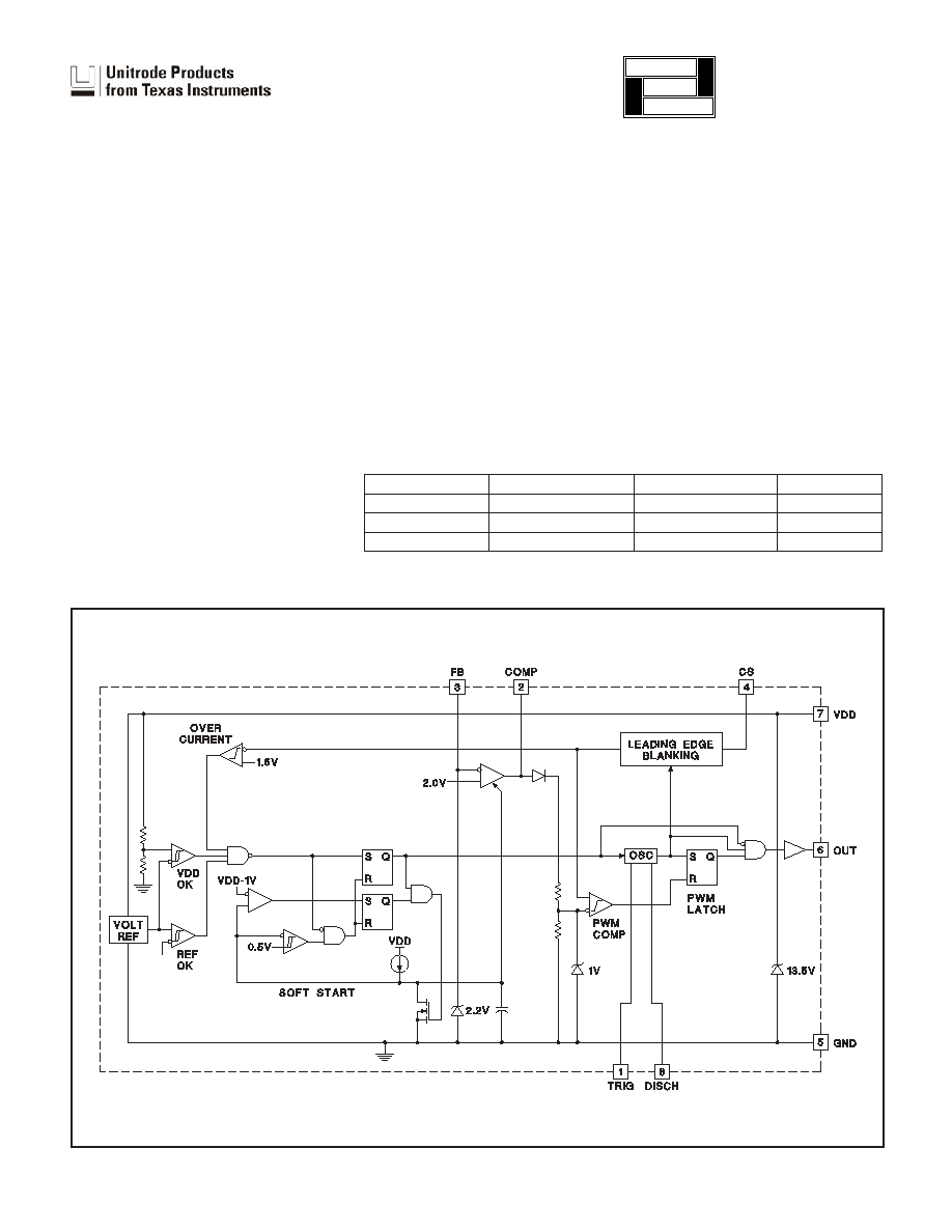
BLOCK DIAGRAM
UDG-95001-1
Part Number
Turn-on Threshold
Turn-off Threshold
Packages
UCCx807-1
7.2V
6.9V
J
UCCx807-2
12.5V
8.3V
N, D
UCCx807-3
4.3V
4.1V
N, D, PW
application
INFO
available
2
UCC1807-1/-2/-3
UCC2807-1/-2/-3
UCC3807-1/-2/-3
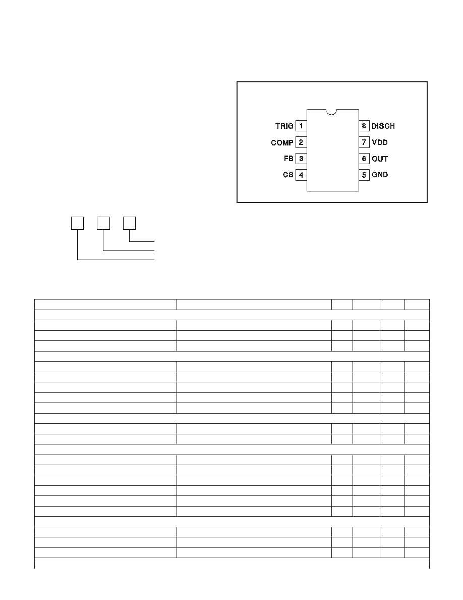
DIL-8, SOIC-8, TSSOP-8 (Top View)
J, N, D or PW Packages
ABSOLUTE MAXIMUM RATINGS
Supply Voltage (I
DD
10mA). . . . . . . . . . . . . . . . . . . . . . . 13.5V
Supply Current . . . . . . . . . . . . . . . . . . . . . . . . . . . . . . . . . 30mA
OUT Current . . . . . . . . . . . . . . . . . . . . . . . . . . . . . . . . . . . . �1A
Analog Inputs (FB, CS) . . . . . . . . . . . . . �0.3V to (VDD + 0.3V)
Power Dissipation at T
A
+25�C (N or J packages) . . . . . . . . 1W
Power Dissipation at T
A
+25�C (D package) . . . . . . . . . . 0.65W
Storage Temperature . . . . . . . . . . . . . . . . . . . �65�C to +150�C
Junction Temperature . . . . . . . . . . . . . . . . . . . �65�C to +150�C
Lead Temperature (Soldering, 10 sec.) . . . . . . . . . . . . . +300�C
All currents are positive into, negative out of the specified ter-
minal. Consult Packaging Section of Databook for thermal limi-
tations and considerations of packages.
CONNECTION DIAGRAMS
ELECTRICAL CHARACTERISTICS:
Unless otherwise stated these specifications apply for T
A
= �55�C to +125�C for
UCC1807-1/-2/-3; �40�C to +85�C for UCC2807-1/-2/-3; and 0�C to +70�C for UCC3807-1/-2/-3; VDD = 10V (Note 6), R
A
= 12k
W
,
R
B
= 4.7k
W
, CT = 330pF, 1.0
m
F capacitor from VDD to GND, T
A
= T
J
.
PARAMETER
TEST CONDITIONS
MIN
TYP
MAX
UNITS
Oscillator Section Section
Frequency
175
202
228
kHz
Temperature Stability
(Note 5)
2.5
%
Amplitude
(Note 1)
1/3VDD
V
Error Amplifier Section
Input Voltage
COMP = 2.0V
1.95
2.00
2.05
V
Input Bias Current
�1
1
m
A
Open Loop Voltage Gain
60
80
dB
COMP Sink Current
FB = 2.2V, COMP = 1.0V
0.3
2.5
mA
COMP Source Current
FB = 1.3V, COMP = 4.0V
�0.2
�0.5
mA
PWM Section
Maximum Duty Cycle
75
78
81
%
Minimum Duty Cycle
COMP = 0V
0
%
Current Sense Section
Gain
(Note 2)
1.1
1.65
1.8
V/V
Maximum Input Signal
COMP = 5.0V (Note 3)
0.9
1.0
1.1
V
Input Bias Current
�200
200
nA
CS Blank Time
50
100
150
ns
Overcurrent Threshold
1.4
1.5
1.6
V
COMP to CS Offset
CS = 0V
0.55
1.1
1.65
V
Output Section
OUT Low Level
I = 100mA
0.4
1
V
OUT High Level
I = �100mA, VDD - OUT
0.4
1
V
Rise/Fall Time
CL = 1nF (Note 5)
20
100
ns
Undervoltage Lockout Section
UCC
807
�
UVLO Threshold
Package
Temperature Range
ORDERING INFORMATION
3
UCC1807-1/-2/-3
UCC2807-1/-2/-3
UCC3807-1/-2/-3
COMP: COMP is the output of the error amplifier and the
input of the PWM comparator. The error amplifier in the
UCC3807 is a low output impedance, 2MHz operational
amplifier. COMP can both source and sink current. The
error amplifier is internally current limited, which allows
zero duty cycle by externally forcing COMP to GND.
The UCC3807 family features built-in full cycle soft start.
Soft start is implemented as a clamp on the maximum
COMP voltage.
CS: Current sense input. There are two current sense
comparators on the chip, the PWM comparator and an
overcurrent comparator.
The UCC3807 also contains a leading edge blanking cir-
cuit, which disconnects the external CS signal from the
current sense comparator during the 100ns interval im-
mediately following the rising edge of the signal at the
OUT pin. In most applications, no analog filtering is re-
quired on CS. Compared to an external RC filtering tech-
nique, leading edge blanking provides a smaller effective
CS to OUT propagation delay. Note, however, that the
minimum non-zero on-time of the OUT signal is directly
affected by the leading edge blanking and the CS to
OUT propagation delay.
The overcurrent comparator is only intended for fault
sensing. Exceeding the overcurrent threshold causes a
soft start cycle.
FB: The inverting input to the error amplifier. For best
stability, keep connections to FB as short as possible and
stray capacitance as small as possible.
GND: Reference ground and power ground for all func-
tions of the part.
OUT: The output of a high current power driver capable
of driving the gate of a power MOSFET with peak cur-
rents exceeding 1A. OUT is actively held low when VDD
is below the UVLO threshold.
The high current power driver consists of MOSFET out-
put devices in a totem pole configuration. This allows the
output to switch from VDD to GND. The output stage
also provides a very low impedance which minimizes
overshoot and undershoot. In most cases, external
Schottky clamp diodes are not required.
PIN DESCRIPTIONS
ELECTRICAL CHARACTERISTICS:
Unless otherwise stated these specifications apply for T
A
= �55�C to +125�C for
UCC1807-1/-2/-3; �40�C to +85�C for UCC2807-1/-2/-3; and 0�C to +70�C for UCC3807-1/-2/-3; VDD = 10V (Note 6), R
A
= 12k
W
,
R
B
= 4.7k
W
, CT = 330pF, 1.0
m
F capacitor from VDD to GND, T
A
= T
J
.
PARAMETER
TEST CONDITIONS
MIN
TYP
MAX
UNITS
Start Threshold
UCCx807-1 (Note 4)
6.6
7.2
7.8
V
UCCx807-2
11.5
12.5
13.5
V
UCCx807-3
4.1
4.3
4.5
V
Minimum Operating Voltage After Start
UCCx807-1 (Note 4)
6.3
6.9
7.5
V
UCCx807-2
7.6
8.3
9.0
V
UCCx807-3
3.9
4.1
4.3
V
Hysteresis
UCCx807-1
0.1
0.3
0.5
V
UCCx807-2
3.5
4.2
5.1
V
UCCx807-3
0.1
0.2
0.3
V
Soft Start Section
COMP Rise Time
FB = 1.8V, From 0.5V to 4.0V
4
ms
Overall Section
Startup Current
VDD < Start Threshold (UCCx807-1,-3)
0.1
0.2
mA
VDD < Start Threshold (UCCx807-2)
0.15
0.25
mA
Operating Supply Current
FB = 0V, CS = 0V, No Load (Note 7)
1.3
2.1
mA
VDD Zener Shunt Voltage
I
DD
= 10mA
12.0
13.5
15.0
V
Shunt to Start Difference
0.5
1.0
V
Note 1: Measured at TRIG; signal minimum = 1/3 VDD, maximum = 2/3 VDD.
Note 2: Gain is defined by: A
V
V
COMP
CS
, 0
V
CS
0.8V
Note 3: Parameter measured at trip point of latch with FB at 0V.
Note 4: Start Threshold and Zener Shunt thresholds track one another.
Note 5: Ensured by design. Not 100% tested in production.
Note 6: Adjust VDD above the start threshold before setting at 10V for UCC3807-2.
Note 7: Does not include current in external timing RC network.
4
UCC1807-1/-2/-3
UCC2807-1/-2/-3
UCC3807-1/-2/-3
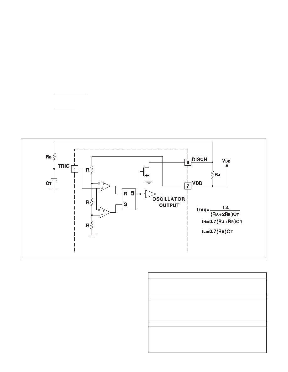
TRIG/DISCH: Oscillator control pins. Trig is the oscillator
timing input, which has an RC-type charge/discharge sig-
nal controlling the chip's internal oscillator. DISCH is the
pin which provides the low impedance discharge path for
the external RC network during normal operation. Oscil-
lator frequency and maximum duty cycle are computed
as follows:
fre que ncy
R
R
C
duty cycle
R
R
R
R
A
B
T
A
B
A
B
1 4
2
2
.
as shown in Figure 1.
For best performance, keep the lead from C
T
to GND as
short as possible. A separate ground connection for C
T
is
desirable. The minimum value of R
A
is 10k
W
, the mini-
mum value of R
B
is 2.2k
W
, and the minimum value of C
T
is 47pF.
VDD: The power input connection for this device. Total
VDD current is the sum of quiescent current and the av-
erage OUT current. Knowing the operating frequency
and the MOSFET gate charge (Qg), average OUT cur-
rent can be calculated from
I
OUT
= Qg
F, where F is frequency.
To prevent noise problems, bypass VDD to GND with a
ceramic capacitor as close to the chip as possible in par-
allel with an electrolytic capacitor.
PIN DESCRIPTIONS (cont.)
Figure 1. Oscillator Block Diagram
UDG-95002-1
T1:
Core
Primary:
Secondary:
Magnetics Inc. #P-42625-UG (ungapped)
28 turns of 2x #26AWG
6 turns of 50x0.2mm Litz wire
L1:
Core:
Main Winding:
Second Winding:
Magnetics Inc. #P-42625-SG-37 (0.020"
gap)
13 turns of 2x #18AWG
11 turns of #26AWG
Magnetics Inc.
900 E. Butler Road
P.O. Box 391
Butler, PA 16003
Tel: (412) 282-8282
Fax: (412) 282-6955
The circuit shown in Fig. 2 illustrates the use of the
UCC3807 in a typical off-line application. The 100W,
200kHz, universal input forward converter produces a
regulated 12VDC at 8 Amps. The programmable maxi-
mum duty cycle of the UCC3807 allows operation down
to 80VRMS and up to 265VRMS with a simple RCD
clamp to limit the MOSFET voltage and provide core re-
set. In this application the maximum duty cycle is set to
about 65%. Another feature of the design is the use of a
flyback winding on the output filter choke for both boot-
strapping and voltage regulation. This method of loop clo-
sure eliminates the optocoupler and secondary side
regulator, common to most off-line designs, while provid-
ing good line and load regulation.
APPLICATIONS INFORMATION

5
UCC1807-1/-2/-3
UCC2807-1/-2/-3
UCC3807-1/-2/-3
Figure 2. Typical Off-line Application Using UCC3807-2
APPLICATIONS INFORMATION (cont.)
UDG-96174

PACKAGING INFORMATION
Orderable Device
Status
(1)
Package
Type
Package
Drawing
Pins Package
Qty
Eco Plan
(2)
Lead/Ball Finish
MSL Peak Temp
(3)
UCC2807D-1
ACTIVE
SOIC
D
8
75
Green (RoHS &
no Sb/Br)
CU NIPDAU
Level-2-260C-1 YEAR
UCC2807D-2
ACTIVE
SOIC
D
8
75
Green (RoHS &
no Sb/Br)
CU NIPDAU
Level-2-260C-1 YEAR
UCC2807D-3
ACTIVE
SOIC
D
8
75
Green (RoHS &
no Sb/Br)
CU NIPDAU
Level-2-260C-1 YEAR
UCC2807DTR-1
ACTIVE
SOIC
D
8
2500 Green (RoHS &
no Sb/Br)
CU NIPDAU
Level-2-260C-1 YEAR
UCC2807DTR-1G4
ACTIVE
SOIC
D
8
2500 Green (RoHS &
no Sb/Br)
CU NIPDAU
Level-2-260C-1 YEAR
UCC2807DTR-2
ACTIVE
SOIC
D
8
2500 Green (RoHS &
no Sb/Br)
CU NIPDAU
Level-2-260C-1 YEAR
UCC2807DTR-2G4
ACTIVE
SOIC
D
8
2500 Green (RoHS &
no Sb/Br)
CU NIPDAU
Level-2-260C-1 YEAR
UCC2807DTR-3
ACTIVE
SOIC
D
8
2500 Green (RoHS &
no Sb/Br)
CU NIPDAU
Level-2-260C-1 YEAR
UCC2807DTR-3G4
ACTIVE
SOIC
D
8
2500 Green (RoHS &
no Sb/Br)
CU NIPDAU
Level-2-260C-1 YEAR
UCC2807N-1
ACTIVE
PDIP
P
8
50
Green (RoHS &
no Sb/Br)
CU NIPDAU
Level-NC-NC-NC
UCC2807N-2
ACTIVE
PDIP
P
8
50
Green (RoHS &
no Sb/Br)
CU NIPDAU
Level-NC-NC-NC
UCC2807PW-3
ACTIVE
TSSOP
PW
14
90
Green (RoHS &
no Sb/Br)
CU NIPDAU
Level-2-260C-1 YEAR
UCC2807PWTR-3
ACTIVE
TSSOP
PW
14
2000 Green (RoHS &
no Sb/Br)
CU NIPDAU
Level-2-260C-1 YEAR
UCC3807D-1
ACTIVE
SOIC
D
8
75
Green (RoHS &
no Sb/Br)
CU NIPDAU
Level-2-260C-1 YEAR
UCC3807D-2
ACTIVE
SOIC
D
8
75
Green (RoHS &
no Sb/Br)
CU NIPDAU
Level-2-260C-1 YEAR
UCC3807D-2G4
ACTIVE
SOIC
D
8
75
Green (RoHS &
no Sb/Br)
CU NIPDAU
Level-2-260C-1 YEAR
UCC3807D-3
ACTIVE
SOIC
D
8
75
Green (RoHS &
no Sb/Br)
CU NIPDAU
Level-2-260C-1 YEAR
UCC3807DTR-1
ACTIVE
SOIC
D
8
2500 Green (RoHS &
no Sb/Br)
CU NIPDAU
Level-2-260C-1 YEAR
UCC3807DTR-2
ACTIVE
SOIC
D
8
2500 Green (RoHS &
no Sb/Br)
CU NIPDAU
Level-2-260C-1 YEAR
UCC3807DTR-2G4
ACTIVE
SOIC
D
8
2500 Green (RoHS &
no Sb/Br)
CU NIPDAU
Level-2-260C-1 YEAR
UCC3807DTR-3
ACTIVE
SOIC
D
8
2500 Green (RoHS &
no Sb/Br)
CU NIPDAU
Level-2-260C-1 YEAR
UCC3807DTR-3G4
ACTIVE
SOIC
D
8
2500 Green (RoHS &
no Sb/Br)
CU NIPDAU
Level-2-260C-1 YEAR
UCC3807N-1
ACTIVE
PDIP
P
8
50
Green (RoHS &
no Sb/Br)
CU NIPDAU
Level-NC-NC-NC
UCC3807N-2
ACTIVE
PDIP
P
8
50
Green (RoHS &
no Sb/Br)
CU NIPDAU
Level-NC-NC-NC
UCC3807N-3
ACTIVE
PDIP
P
8
50
Green (RoHS &
no Sb/Br)
CU NIPDAU
Level-NC-NC-NC
PACKAGE OPTION ADDENDUM
www.ti.com
4-Nov-2005
Addendum-Page 1

Orderable Device
Status
(1)
Package
Type
Package
Drawing
Pins Package
Qty
Eco Plan
(2)
Lead/Ball Finish
MSL Peak Temp
(3)
UCC3807N-3G4
ACTIVE
PDIP
P
8
50
Green (RoHS &
no Sb/Br)
CU NIPDAU
Level-NC-NC-NC
UCC3807PWTR-3
PREVIEW
TSSOP
PW
14
2000
TBD
Call TI
Call TI
(1)
The marketing status values are defined as follows:
ACTIVE: Product device recommended for new designs.
LIFEBUY: TI has announced that the device will be discontinued, and a lifetime-buy period is in effect.
NRND: Not recommended for new designs. Device is in production to support existing customers, but TI does not recommend using this part in
a new design.
PREVIEW: Device has been announced but is not in production. Samples may or may not be available.
OBSOLETE: TI has discontinued the production of the device.
(2)
Eco
Plan
-
The
planned
eco-friendly
classification:
Pb-Free
(RoHS)
or
Green
(RoHS
&
no
Sb/Br)
-
please
check
http://www.ti.com/productcontent
for the latest availability information and additional product content details.
TBD: The Pb-Free/Green conversion plan has not been defined.
Pb-Free (RoHS): TI's terms "Lead-Free" or "Pb-Free" mean semiconductor products that are compatible with the current RoHS requirements
for all 6 substances, including the requirement that lead not exceed 0.1% by weight in homogeneous materials. Where designed to be soldered
at high temperatures, TI Pb-Free products are suitable for use in specified lead-free processes.
Green (RoHS & no Sb/Br): TI defines "Green" to mean Pb-Free (RoHS compatible), and free of Bromine (Br) and Antimony (Sb) based flame
retardants (Br or Sb do not exceed 0.1% by weight in homogeneous material)
(3)
MSL, Peak Temp. -- The Moisture Sensitivity Level rating according to the JEDEC industry standard classifications, and peak solder
temperature.
Important Information and Disclaimer:The information provided on this page represents TI's knowledge and belief as of the date that it is
provided. TI bases its knowledge and belief on information provided by third parties, and makes no representation or warranty as to the
accuracy of such information. Efforts are underway to better integrate information from third parties. TI has taken and continues to take
reasonable steps to provide representative and accurate information but may not have conducted destructive testing or chemical analysis on
incoming materials and chemicals. TI and TI suppliers consider certain information to be proprietary, and thus CAS numbers and other limited
information may not be available for release.
In no event shall TI's liability arising out of such information exceed the total purchase price of the TI part(s) at issue in this document sold by TI
to Customer on an annual basis.
PACKAGE OPTION ADDENDUM
www.ti.com
4-Nov-2005
Addendum-Page 2
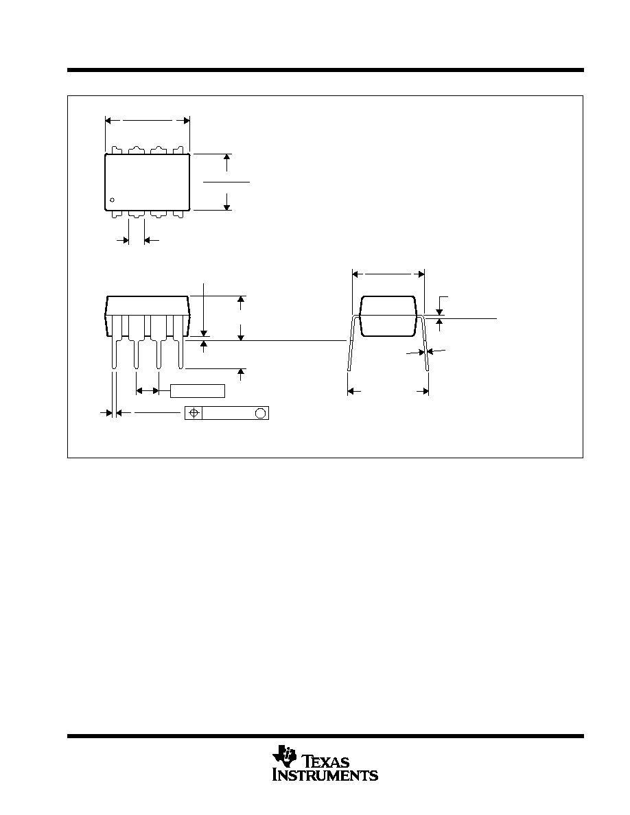
MECHANICAL DATA
MPDI001A � JANUARY 1995 � REVISED JUNE 1999
POST OFFICE BOX 655303
�
DALLAS, TEXAS 75265
P (R-PDIP-T8)
PLASTIC DUAL-IN-LINE
8
4
0.015 (0,38)
Gage Plane
0.325 (8,26)
0.300 (7,62)
0.010 (0,25) NOM
MAX
0.430 (10,92)
4040082/D 05/98
0.200 (5,08) MAX
0.125 (3,18) MIN
5
0.355 (9,02)
0.020 (0,51) MIN
0.070 (1,78) MAX
0.240 (6,10)
0.260 (6,60)
0.400 (10,60)
1
0.015 (0,38)
0.021 (0,53)
Seating Plane
M
0.010 (0,25)
0.100 (2,54)
NOTES: A. All linear dimensions are in inches (millimeters).
B. This drawing is subject to change without notice.
C. Falls within JEDEC MS-001
For the latest package information, go to http://www.ti.com/sc/docs/package/pkg_info.htm

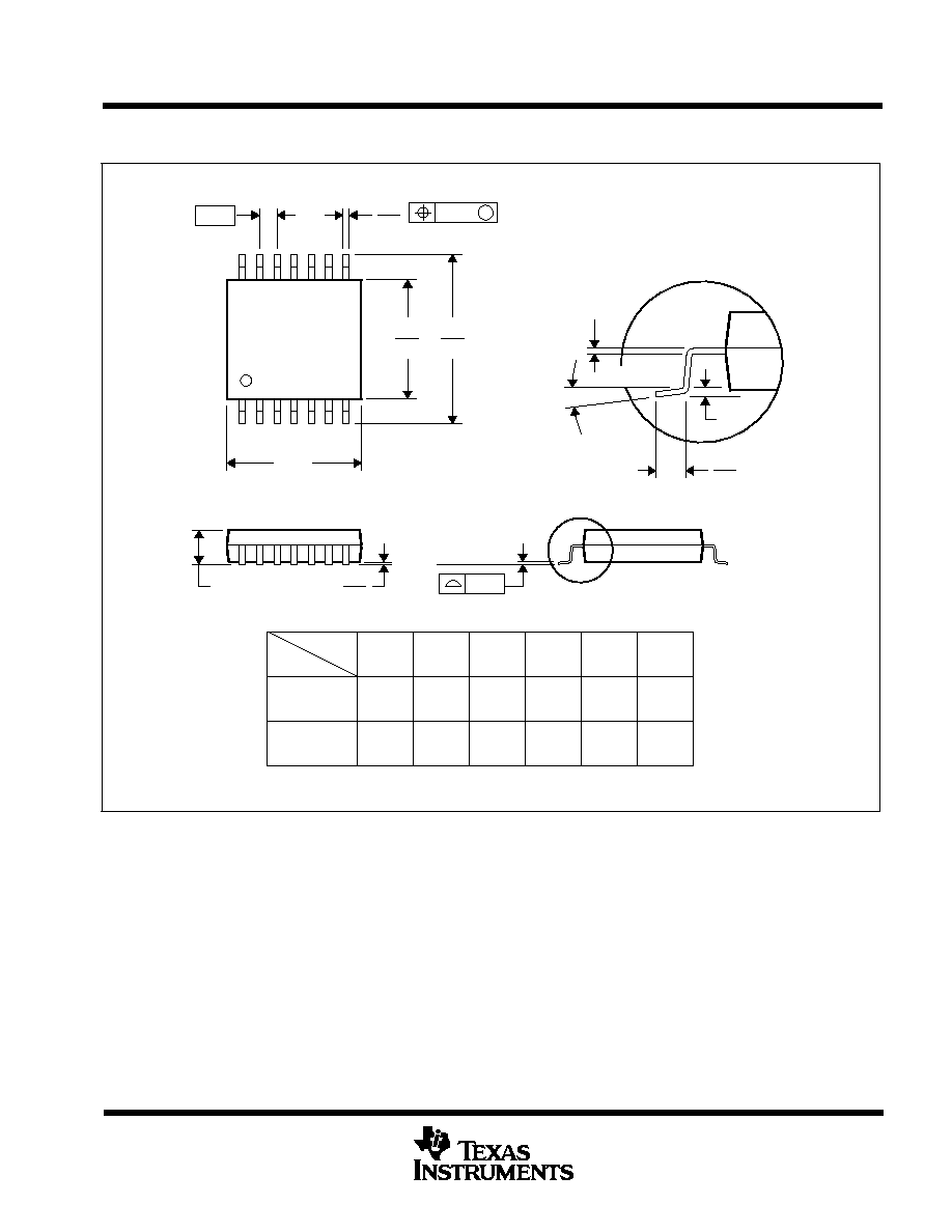
MECHANICAL DATA
MTSS001C � JANUARY 1995 � REVISED FEBRUARY 1999
POST OFFICE BOX 655303
�
DALLAS, TEXAS 75265
PW (R-PDSO-G**)
PLASTIC SMALL-OUTLINE PACKAGE
14 PINS SHOWN
0,65
M
0,10
0,10
0,25
0,50
0,75
0,15 NOM
Gage Plane
28
9,80
9,60
24
7,90
7,70
20
16
6,60
6,40
4040064/F 01/97
0,30
6,60
6,20
8
0,19
4,30
4,50
7
0,15
14
A
1
1,20 MAX
14
5,10
4,90
8
3,10
2,90
A MAX
A MIN
DIM
PINS **
0,05
4,90
5,10
Seating Plane
0
�
� 8
�
NOTES: A. All linear dimensions are in millimeters.
B. This drawing is subject to change without notice.
C. Body dimensions do not include mold flash or protrusion not to exceed 0,15.
D. Falls within JEDEC MO-153

IMPORTANT NOTICE
Texas Instruments Incorporated and its subsidiaries (TI) reserve the right to make corrections, modifications,
enhancements, improvements, and other changes to its products and services at any time and to discontinue
any product or service without notice. Customers should obtain the latest relevant information before placing
orders and should verify that such information is current and complete. All products are sold subject to TI's terms
and conditions of sale supplied at the time of order acknowledgment.
TI warrants performance of its hardware products to the specifications applicable at the time of sale in
accordance with TI's standard warranty. Testing and other quality control techniques are used to the extent TI
deems necessary to support this warranty. Except where mandated by government requirements, testing of all
parameters of each product is not necessarily performed.
TI assumes no liability for applications assistance or customer product design. Customers are responsible for
their products and applications using TI components. To minimize the risks associated with customer products
and applications, customers should provide adequate design and operating safeguards.
TI does not warrant or represent that any license, either express or implied, is granted under any TI patent right,
copyright, mask work right, or other TI intellectual property right relating to any combination, machine, or process
in which TI products or services are used. Information published by TI regarding third-party products or services
does not constitute a license from TI to use such products or services or a warranty or endorsement thereof.
Use of such information may require a license from a third party under the patents or other intellectual property
of the third party, or a license from TI under the patents or other intellectual property of TI.
Reproduction of information in TI data books or data sheets is permissible only if reproduction is without
alteration and is accompanied by all associated warranties, conditions, limitations, and notices. Reproduction
of this information with alteration is an unfair and deceptive business practice. TI is not responsible or liable for
such altered documentation.
Resale of TI products or services with statements different from or beyond the parameters stated by TI for that
product or service voids all express and any implied warranties for the associated TI product or service and
is an unfair and deceptive business practice. TI is not responsible or liable for any such statements.
Following are URLs where you can obtain information on other Texas Instruments products and application
solutions:
Products
Applications
Amplifiers
amplifier.ti.com
Audio
www.ti.com/audio
Data Converters
dataconverter.ti.com
Automotive
www.ti.com/automotive
DSP
dsp.ti.com
Broadband
www.ti.com/broadband
Interface
interface.ti.com
Digital Control
www.ti.com/digitalcontrol
Logic
logic.ti.com
Military
www.ti.com/military
Power Mgmt
power.ti.com
Optical Networking
www.ti.com/opticalnetwork
Microcontrollers
microcontroller.ti.com
Security
www.ti.com/security
Telephony
www.ti.com/telephony
Video & Imaging
www.ti.com/video
Wireless
www.ti.com/wireless
Mailing Address:
Texas Instruments
Post Office Box 655303 Dallas, Texas 75265
Copyright
2005, Texas Instruments Incorporated