UCC1809-1/-2
UCC2809-1/-2
UCC3809-1/-2
SLUS166A - NOVEMBER 1999
FEATURES
∑ User Programmable Soft Start With
Active Low Shutdown
∑ User Programmable Maximum Duty
Cycle
∑ Accessible 5V Reference
∑ Undervoltage Lockout
∑ Operation to 1MHz
∑ 0.4A Source/0.8A Sink FET Driver
∑ Low 100µA Startup Current
Economy Primary Side Controller
1
3
2
7
FB
1V
6
µA
+5V
0.5V
OSC
4
R
Q
S
5V
REF
15/8V
10/8V
VDD
8
REF
C
REF
C
VDD
5
V
REF
SS
RT1
RT2
C
SS
DISABLE
NOISE
FILTER
SLOPE
COMP
CURRENT
SENSE
FEEDBACK
R
START
V
IN
CLK
PWM
LATCH
UVLO
1V
V
OUT
C
T
6
17.5V
OUT
GND
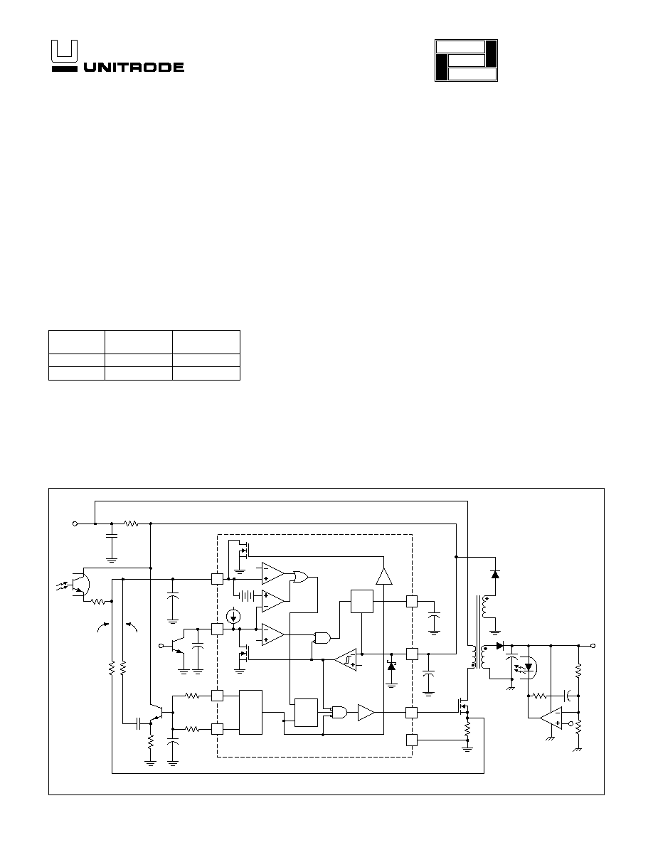
TYPICAL APPLICATION DIAGRAM
UDG-99036
DESCRIPTION
The UCC3809 family of BCDMOS economy low power integrated circuits
contains all the control and drive circuitry required for off-line and isolated
DC-to-DC fixed frequency current mode switching power supplies with
minimal external parts count. Internally implemented circuits include
undervoltage lockout featuring startup current less than 100
µA, a user ac-
cessible voltage reference, logic to ensure latched operation, a PWM com-
parator, and a totem pole output stage to sink or source peak current. The
output stage, suitable for driving N-Channel MOSFETs, is low in the off
state.
Oscillator frequency and maximum duty cycle are programmed with two
resistors and a capacitor. The UCC3809 family also features full cycle soft
start.
The family has UVLO thresholds and hysteresis levels for off-line and
DC-to-DC systems as shown in the table to the left.
The UCC3809 and the UCC2809 are offered in the 8 pin SOIC (D), PDIP
(N), TSSOP (PW), and MSOP (P) packages. The small TSSOP and
MSOP packages make the device ideal for applications where board
space and height are at a premium.
PART
NUMBER
TURN ON
THRESHOLD
TURN OFF
THRESHOLD
UCCX809-1
10V
8V
UCCX809-2
15V
8V
application
INFO
available
2
UCC1809-1/-2
UCC2809-1/-2
UCC3809-1/-2
CONNECTION DIAGRAM
Temperature Range Available Packages
UCC1809-X
≠55∞C to +125∞C
J
UCC2809-X
≠40∞C to +85∞C
N, D, P, PW
UCC3809-X
0∞C to +70∞C
N, D, P, PW
ELECTRICAL CHARACTERISTICS
: Unless otherwise specified, VDD = 12V. T
A
= T
J
.
PARAMETER
TEST CONDITIONS
MIN
TYP
MAX
UNIT
Supply Section
VDD Clamp
I
VDD
= 10mA
16
17.5
19
V
I
VDD
No Load
600
900
µA
I
VDD
Starting
100
µA
Undervoltage Lockout Section
Start Threshold (UCCx809-1)
9.4
10.4
V
UVLO Hysteresis (UCCx809-1)
1.65
V
Start Threshold (UCCx809-2)
14.0
15.6
V
UVLO Hysteresis (UCCx809-2)
6.2
V
Voltage Reference Section
Output Voltage
I
REF
= 0mA
4.75
5
5.25
V
Line Regulation
VDD = 10V to 15V
2
mV
Load Regulation
I
REF
= 0mA to 5mA
2
mV
Comparator Section
I
FB
Output Off
≠100
nA
Comparator Threshold
0.9
0.95
1
V
OUT Propagation Delay (No Load)
V
FB
= 0.8V to 1.2V at T
R
= 10ns
50
100
ns
SOIC-8, DIL-8 (Top View)
D, N and J Packages
ABSOLUTE MAXIMUM RATINGS*
VDD . . . . . . . . . . . . . . . . . . . . . . . . . . . . . . . . . . . . . . . . . . . 19V
I
VDD
. . . . . . . . . . . . . . . . . . . . . . . . . . . . . . . . . . . . . . . . . . 25mA
I
OUT
(tpw < 1
µs and Duty Cycle < 10%). . . . . . . . ≠0.4A to 0.8A
RT1, RT2, SS . . . . . . . . . . . . . . . . . . . . . . ≠0.3V to REF + 0.3V
I
REF
. . . . . . . . . . . . . . . . . . . . . . . . . . . . . . . . . . . . . . . . . ≠15mA
Storage Temperature . . . . . . . . . . . . . . . . . . . ≠65∞C to +150∞C
Junction Temperature . . . . . . . . . . . . . . . . . . . ≠55∞C to +150∞C
Lead Temperature (Soldering, 10 sec.) . . . . . . . . . . . . . +300∞C
* Values beyond which damage may occur.
All voltages are with respect to ground unless otherwise stated.
Currents are positive into, negative out of the specified termi-
nal. Consult Packaging Section of Databook for thermal limita-
tions and considerations of packages.
UCC
809
≠
ORDERING INFORMATION
FB
SS
RT1
RT2
REF
VDD
OUT
GND
8
7
6
5
1
2
3
4
TSSOP-8 (Top View)
PW Package
FB
2
1
4
3
7
8
5
6
SS
RT1
RT2
REF
VDD
OUT
GND
MSOP-8 (Top View)
P Package
3
UCC1809-1/-2
UCC2809-1/-2
UCC3809-1/-2
PIN DESCRIPTIONS
FB: This pin is the summing node for current sense
feedback, voltage sense feedback (by optocoupler) and
slope compensation. Slope compensation is derived
from the rising voltage at the timing capacitor and can be
buffered with an external small signal NPN transistor.
External high frequency filter capacitance applied from
this node to GND is discharged by an internal 250
on
resistance NMOS FET during PWM off time and offers
effective leading edge blanking set by the RC time
constant of the feedback resistance from current sense
resistor to FB input and the high frequency filter
capacitor capacitance at this node to GND.
GND: Reference ground and power ground for all
functions.
OUT: This pin is the high current power driver output. A
minimum series gate resistor of 3.9
is recommended to
limit the gate drive current when operating with high bias
voltages.
REF: The internal 5V reference output. This reference is
buffered and is available on the REF pin. REF should be
bypassed with a 0.47
µF ceramic capacitor.
RT1: This pin connects to timing resistor RT1 and
controls the positive ramp time of the internal oscillator
(Tr = 0.74
∑ (C
T
+ 27pF)
∑ RT1). The positive threshold
of the internal oscillator is sensed through inactive timing
resistor RT2 which connects to pin RT2 and timing
capacitor C
T
.
RT2: This pin connects to timing resistor RT2 and
controls the negative ramp time of the internal oscillator
(Tf = 0.74
∑ (C
T
+ 27pF)
∑ RT2). The negative threshold
of the internal oscillator is sensed through inactive timing
resistor RT1 which connects to pin RT1 and timing
capacitor C
T
.
SS: This pin serves two functions. The soft start timing
capacitor connects to SS and is charged by an internal
6
µA current source. Under normal soft start SS is
discharged to at least 0.4V and then ramps positive to
1V during which time the output driver is held low. As SS
charges from 1V to 2V soft start is implemented by an
increasing output duty cycle. If SS is taken below 0.5V,
the output driver is inhibited and held low. The user
accessible 5V voltage reference also goes low and I
VDD
< 100
µA.
VDD: The power input connection for this device. This
pin is shunt regulated at 17.5V which is sufficiently below
the voltage rating of the DMOS output driver stage. VDD
should be bypassed with a 1
µF ceramic capacitor.
ELECTRICAL CHARACTERISTICS
: Unless otherwise specified, VDD = 12V. T
A
= T
J
.
PARAMETER
TEST CONDITIONS
MIN
TYP
MAX
UNIT
Soft Start Section
I
SS
VDD = 16V, V
SS
= 0V; ≠40
∞C to +85∞C
≠4.9
≠7.0
≠9.1
µA
VDD = 16V, V
SS
= 0V;
< ≠40∞C; >+85∞C
≠4.0
≠7.0
≠10.0
µA
V
SS
Low
VDD = 7.5V, I
SS
= 200
µA
0.2
V
Shutdown Threshold
0.44
0.48
0.52
V
Oscillator Section
Frequency
RT1 = 10k, RT2 = 4.32k, CT = 820pF
90
100
110
kHz
Frequency Change with Voltage
VDD = 10V to 15V
0.1
%/V
C
T
Peak Voltage
3.33
V
C
T
Valley Voltage
1.67
V
C
T
Peak to Peak Voltage
1.54
1.67
1.80
V
Output Section
Output V
SAT
Low
I
OUT
= 80mA (dc)
0.8
1.5
V
Output V
SAT
High
I
OUT
= ≠40mA (dc), VDD ≠ OUT
0.8
1.5
V
Output Low Voltage During UVLO
I
OUT
= 20mA (dc)
1.5
V
Minimum Duty Cycle
V
FB
= 2V
0
%
Maximum Duty Cycle
70
%
Rise Time
C
OUT
= 1nF
35
ns
Fall Time
C
OUT
= 1nF
18
ns
4
UCC1809-1/-2
UCC2809-1/-2
UCC3809-1/-2
UDG-99179
T1
80
µ
H
5:1
C1
0
0.22
µ
F
R9
2K
3W
R1
3
1.1K
R1
1
680
Q3
IR
F
6
40
D3
SF24
Q2
2N
2907A
D4
1N
5240
8
7
6
5
4
3
2
1
UCC3
8
0
9
U1
FB
RE
F
SS
RT
1
RT
2
VD
D
OUT
GND
C8
1
µ
F
C9
0.1
µ
F
C7
0.47
µ
F
TP1
R5
470
R2
0
5.62K
C2
2
0.1
µ
F
Q4
2N
2222A
R1
8
3.01K
C6
330pF
D1
5231B
D2
1N
5245
R7
15K
R6
1K
R8
0.15
3W
R4
6.19K
R3
12.1K
C5
1nF
C4
0.01
µ
F
Q1
2N
2222A
R2
1.1K
ON/
O
FF
≠VIN
C3
1
µ
F
+VIN
C2
150
µ
F
C1
150
µ
F
R1
2
27K
R1
5
10K
C1
4
470pF
R1
6
12.1K
1%
U4
T
L431
H1
1
A
V
1
U3
2
1
4
5
R1
7
12.1K
1%
C1
3
0.1
µ
F
C1
5
0.015
µ
F
R1
9
5.1K
3W
U2
M
B
R
2535C
T
L
1
3
2
C1
6
330
µ
F
6.3V
C1
7
330
µ
F
6.3V
C1
8
330
µ
F
6.3V
C1
9
330
µ
F
6.3V
R1
4
750
+V
OUT
≠V
OUT
R1
5.1k
R1
0
10
P
G
ND1
P
G
ND1
APPLICATION INFORMATION
Figure 1. Isolated 50W flyback converter utilizing the UCC3809. The switching frequency is 70kHz, Vin = -32V
to -72V, Vout = +5V, Iout = 0A to 10A
5
UCC1809-1/-2
UCC2809-1/-2
UCC3809-1/-2
The Typical Application Diagram shows an isolated
flyback converter utilizing the UCC3809. Note that the
capacitors C
REF
and C
VDD
are local decoupling capaci-
tors for the reference and IC input voltage, respectively.
Both capacitors should be low ESR and ESL ceramic,
placed as close to the IC pins as possible, and returned
directly to the ground pin of the chip for best stability.
REF provides the internal bias to many of the IC func-
tions and C
REF
should be at least 0.47
µF to prevent REF
from drooping.
FB Pin
The basic premise of the UCC3809 is that the voltage
sense feedback signal originates from an optocoupler
that is modulated by an external error amplifier located
on the secondary side. This signal is summed with the
current sense signal and any slope compensation at the
FB pin and compared to a 1V threshold, as shown in the
Typical Application Diagram. Crossing this 1V threshold
resets the PWM latch and modulates the output driver
on-time much like the current sense comparator used in
the UC3842. In the absence of a FB signal, the output
will follow the programmed maximum on-time of the os-
cillator.
When adding slope compensation, it is important to use
a small capacitor to AC couple the oscillator waveform
before summing this signal into the FB pin. By correctly
selecting the emitter resistor of the optocoupler, the volt-
age sense signal can force the FB node to exceed the
1V threshold when the output that is being compared ex-
ceeds a desired level. Doing so drives the UCC3809 to
zero percent duty cycle.
Oscillator
The following equation sets the oscillator frequency:
(
) (
)
[
]
F
CT
pF
RT
RT
OSC
=
∑
+
∑
+
-
0 74
27
1
2
1
.
(
)
D
RT
CT
pF
F
MAX
OSC
=
∑
∑
+
∑
0 74
1
27
.
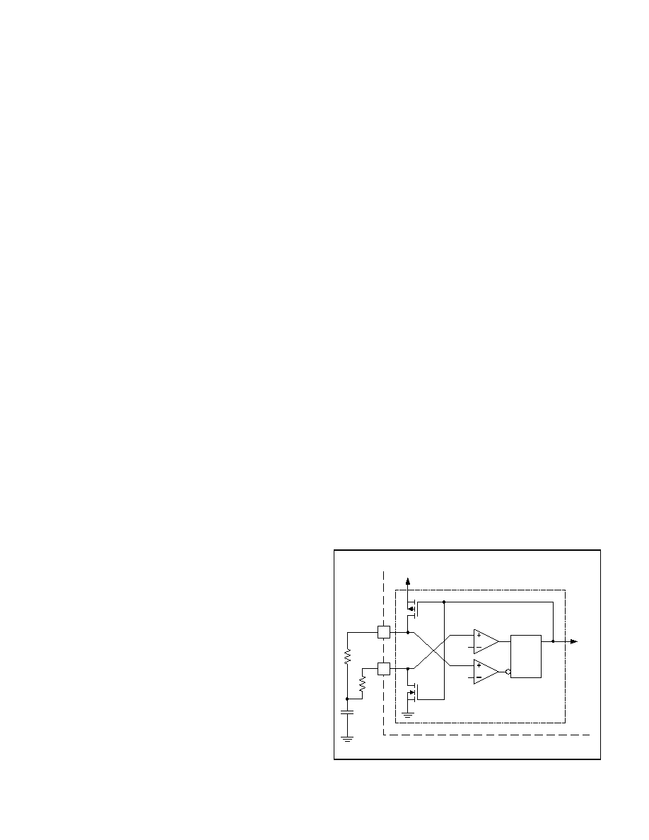
Referring to Figure 2 and the waveforms in Figure 3,
when Q1is on, CT charges via the R
DS(on)
of Q1 and
RT1. During this charging process, the voltage of CT is
sensed through RT2. The S input of the oscillator latch,
S(OSC), is level sensitive, so crossing the upper thresh-
old (set at 2/3 VREF or 3.33V for a typical 5.0V refer-
ence) sets the Q output (CLK signal) of the oscillator
latch high. A high CLK signal results in turning off Q1
and turning on Q2. CT now discharges through RT2 and
the R
DS(on)
of Q2.
CT discharges from 3.33V to the
lower threshold (set at 1/3 VREF or 1.67V for a typical
5.0V reference) sensed through RT1. The R input to the
oscillator latch, R(OSC), is also level sensitive and resets
the CLK signal low when CT crosses the 1.67V thresh-
old, turning off Q2 and turning on Q1, initiating another
charging cycle.
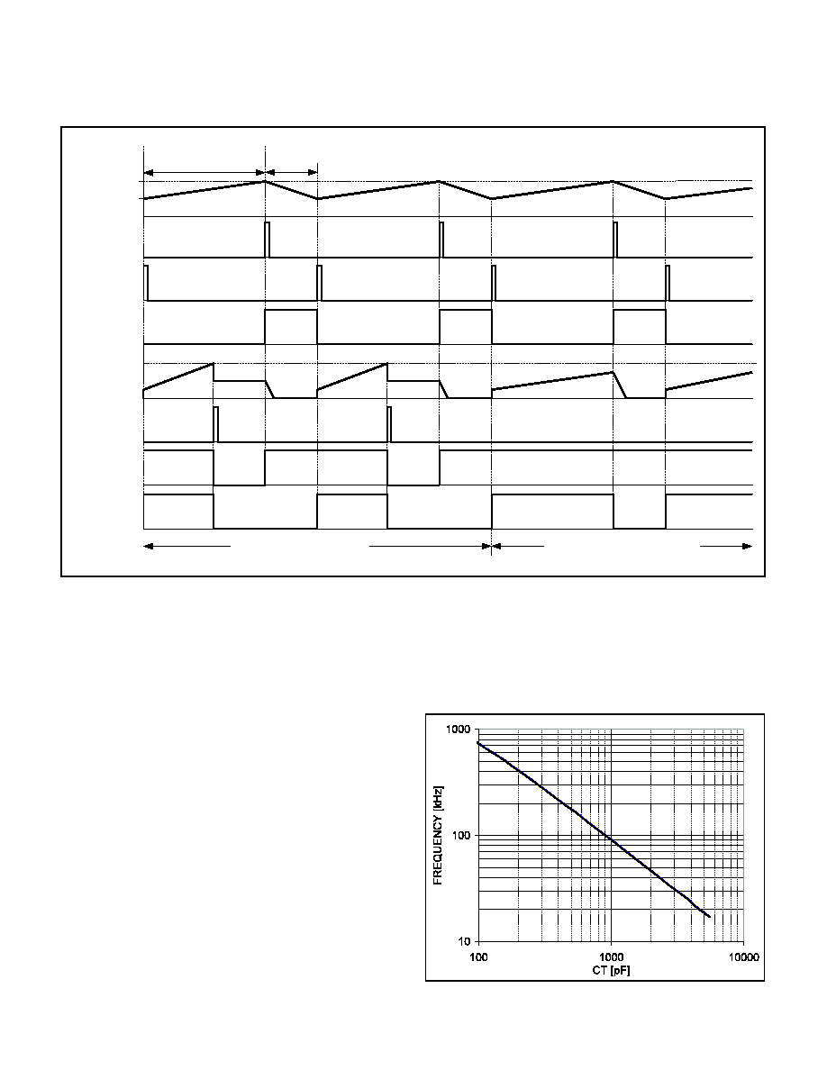
Figure 3 shows the waveforms associated with the oscil-
lator latch and the PWM latch (shown in the Typical Ap-
plication Diagram). A high CLK signal not only initiates a
discharge cycle for CT, it also turns on the internal
NMOS FET on the FB pin causing any external capaci-
tance used for leading edge blanking connected to this
pin to be discharged to ground. By discharging any ex-
ternal capacitor completely to ground during the external
switch's off-time, the noise immunity of the converter is
enhanced allowing the user to design in smaller RC com-
ponents for leading edge blanking. A high CLK signal
also sets the level sensitive S input of the PWM latch,
S(PWM), high, resulting in a high output, Q(PWM), as
shown in Figure 3. This Q(PWM) signal will remain high
until a reset signal, R(PWM) is received. A high R(PWM)
signal results from the FB signal crossing the 1V thresh-
old, or during soft start or if the SS pin is disabled.
Assuming the UVLO threshold is satisfied, the OUT sig-
nal of the IC will be high as long as Q(PWM) is high and
S(PWM), also referred to as CLK, is low. The OUT sig-
nal will be dominated by the FB signal as long as the FB
signal trips the 1V threshold while CLK is low. If the FB
signal does not cross the 1V threshold while CLK is low,
the OUT signal will be dominated by the maximum duty
cycle programmed by the user. Figure 3 illustrates the
various waveforms for a design set up for a maximum
duty cycle of 70%.
APPLICATION INFORMATION (cont.)
S
Q
R
Q2
Q1
3
4
RT2
CT
RT1
V
REF
3.33V
1.67V
CLK
OSC
OSCILLATOR
LATCH
Figure 2. UCC3809 oscillator.
UDG-97195
6
UCC1809-1/-2
UCC2809-1/-2
UCC3809-1/-2
The recommended value for CT is 1nF for frequencies in
the 100 kHz or less range and smaller CT for higher fre-
quencies. The minimum recommended values of RT1
and RT2 are 10k
and 4.32k, respectively. Using these
values maintains a ratio of at least 20:1 between the
R
DS(on)
of the internal FETs and the external timing re-
sistors, resulting in minimal change in frequency over
temperature. Because of the oscillator's susceptibility to
capacitive coupling, examine the oscillator frequency by
looking at the common RT1-RT2-CT node on the circuit
board as opposed to looking at pins 3 and 4 directly. For
good noise immunity, RT1 and RT2 should be placed as
close to pins 3 and 4 of the IC as possible. CT should be
returned directly to the ground pin of the IC with minimal
stray inductance and capacitance.
Figure 4. Oscillator frequency vs. C
T
(RT1 = 10k,
RT2 = 4.32k)
CT
S(OSC)
R(OSC)
Q(OSC)=CLK
=S(PWM)
FB
R(PWM)
Q(PWM)
OUT
CT
CHARGING
CT
DISCHARGING
3.33V
1.67V
1V
70%
ON
30%
OFF
FB SIGNAL DOMINANT
MAX. DUTY CYCLE DOMINANT
Figure 3. Waveforms associated with the oscillator latch and the PWM latch.
APPLICATION INFORMATION (cont.)
UDG-99037
7
UCC1809-1/-2
UCC2809-1/-2
UCC3809-1/-2
UNITRODE CORPORATION
7 CONTINENTAL BLVD. ∑ MERRIMACK, NH 03054
TEL. (603) 424-2410 ∑ FAX (603) 424-3460
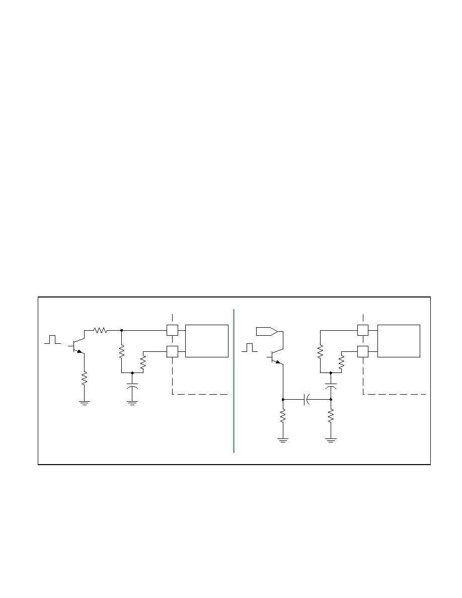
3
4
UCC3809
OSCILLATOR
RT2
CT
RT1
1k
2N2222A
424
SYNC
PULSE
OPTION I
3
4
UCC3809
OSCILLATOR
RT2
CT
RT1
424
SYNC
PULSE
0.1
µF
2N2222A
24
+5V
OPTION II
Figure 5. UCC3809 synchronization options.
UDG-99006
Synchronization
Both of the synchronization schemes shown in Figure 5
can be successfully implemented with the internal oscilla-
tor of the UCC3809. Both schemes allow access to the
timing ramp needed for slope compensation and have
minimal impact on the programmed maximum duty cycle.
In the absence of a sync pulse, the PWM controller will
run independently at the frequency set by RT1, RT2, and
CT. This free running frequency must be approximately
15 to 20% lower than the sync pulse frequency to insure
the free running oscillator does not cross the comparator
threshold before the desired sync pulse.
Option I uses the synchronization pulse to pull pin 3 low,
triggering the internal 1.67V comparator to reset the RS
latch and initiate a charging cycle. The valley voltage of
the CT waveform is higher when synchronized using this
configuration, decreasing the ramp charge and discharge
times, thereby increasing the operating frequency; other-
wise the overall shape of the CT voltage waveform is un-
changed.
Option II uses the synchronization pulse to superimpose
the sync voltage onto the peak of the CT waveform. This
triggers the internal 3.33V comparator, initiating a dis-
charge cycle. The sync pulse is summed with the free
running oscillator waveform at the CT node, resulting in a
spike on top of the CT peak voltage.
ADDITIONAL INFORMATION
Please refer to the following Unitrode application topics
for additional information.
[1] Application Note U-165,
Design Review: Isolated 50W
Flyback Converter with the UCC3809 Primary Side Con-
troller
by Lisa Dinwoodie.
[2]
Design
Note
DN-89,
Comparing
the
UC3842,
UCC3802, and UCC3809 Primary Side PWM Controllers
by Lisa Dinwoodie.
APPLICATION INFORMATION (cont.)

IMPORTANT NOTICE
Texas Instruments and its subsidiaries (TI) reserve the right to make changes to their products or to discontinue
any product or service without notice, and advise customers to obtain the latest version of relevant information
to verify, before placing orders, that information being relied on is current and complete. All products are sold
subject to the terms and conditions of sale supplied at the time of order acknowledgment, including those
pertaining to warranty, patent infringement, and limitation of liability.
TI warrants performance of its semiconductor products to the specifications applicable at the time of sale in
accordance with TI's standard warranty. Testing and other quality control techniques are utilized to the extent
TI deems necessary to support this warranty. Specific testing of all parameters of each device is not necessarily
performed, except those mandated by government requirements.
Customers are responsible for their applications using TI components.
In order to minimize risks associated with the customer's applications, adequate design and operating
safeguards must be provided by the customer to minimize inherent or procedural hazards.
TI assumes no liability for applications assistance or customer product design. TI does not warrant or represent
that any license, either express or implied, is granted under any patent right, copyright, mask work right, or other
intellectual property right of TI covering or relating to any combination, machine, or process in which such
semiconductor products or services might be or are used. TI's publication of information regarding any third
party's products or services does not constitute TI's approval, warranty or endorsement thereof.
Copyright
©
2000, Texas Instruments Incorporated