 | –≠–ª–µ–∫—Ç—Ä–æ–Ω–Ω—ã–π –∫–æ–º–ø–æ–Ω–µ–Ω—Ç: UCC2810N | –°–∫–∞—á–∞—Ç—å:  PDF PDF  ZIP ZIP |
Document Outline
- FEATURES
- DESCRIPTION
- ORDERING INFORMATION
- ABSOLUTE MAXIMUM RATINGS
- BLOCK DIAGRAM
- ELECTRICAL CHARACTERISTICS
- DEVICE INFORMATION
- APPLICATION INFORMATION
- timing resistor
- leading edge blanking and current sense
- oscillator
- error amplifier output stage
- TYPICAL CHARACTERISTICS
- PACKAGE DRAWINGS
- DW (R-PDSO-G**) PLASTIC SMALL-OUTLINE PACKAGE
- J (R-GDIP-T**) CERAMIC DUAL-IN-LINE
- N (R-PDIP-T**) PLASTIC DUAL-IN-LINE PACKAGE
- IMPORTANT NOTICE
UCC2810, UCC2811
UCC3810, UCC3811
SLUS162A ≠ FEBRUARY 1999 ≠ REVISED OCTOBER 2002
DUAL CHANNEL SYNCHRONIZED
CURRENT-MODE PWM
1
www.ti.com
FEATURES
D
Single Oscillator Synchronizes Two PWMs
D
150-
µ
A Startup Supply Current
D
2-mA Operating Supply Current
D
Operation to 1 MHz
D
Internal Soft-Start
D
Full-Cycle Fault Restart
D
Internal Leading-Edge Blanking of the
Current Sense Signal
D
1-A Totem Pole Outputs
D
75-ns Typical Response from Current Sense
to Output
D
1.5% Tolerance Voltage Reference
D
Two UVLO Options
1
2
3
4
5
6
7
8
16
15
14
13
12
11
10
9
SYNC
CT
RT
FB1
COMP1
CS1
OUT1
GND
VCC
REF
ENABLE2
FB2
COMP2
CS2
OUT2
PWRGND
DW PACKAGE
(TOP VIEW)
1
2
3
4
5
6
7
8
16
15
14
13
12
11
10
9
SYNC
CT
RT
FB1
COMP1
CS1
OUT1
GND
VCC
REF
ENABLE2
FB2
COMP2
CS2
OUT2
PWRGND
N PACKAGE
(TOP VIEW)
DESCRIPTION
The UCC3810 and UCC3811 are high-speed
BiCMOS integrated circuits implementing two
synchronized pulse width modulators for use in
off-line and dc-to-dc power supplies. The
UCC381x family provides perfect synchronization
between two PWMs by using the same oscillator.
The oscillator's sawtooth waveform can be used
for slope compensation if required.
Using a toggle flip-flop to alternate between
modulators, the UCC3810 ensures that one PWM
does not slave, interfere, or otherwise affect the
other PWM. This toggle flip- flop also ensures that
each PWM is limited to 50% maximum duty cycle,
insuring adequate off-time to reset magnetic
elements. This device contains many of the same
elements of the UC3842 current mode controller
family, combined with the enhancements of the
UCC3802. This minimizes power supply parts
count. Enhancements include leading edge
blanking of the current sense signals, full cycle
fault restart, CMOS output drivers, and outputs
which remain low even when the supply voltage is
removed.
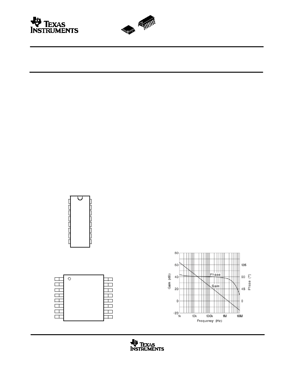
ERROR AMPLIFIER GAIN AND PHASE
vs
FREQUENCY
PRODUCTION DATA information is current as of publication date.
Products conform to specifications per the terms of Texas Instruments
standard warranty. Production processing does not necessarily include
testing of all parameters.
Copyright
2002, Texas Instruments Incorporated
UCC2810, UCC2811
UCC3810, UCC3811
SLUS162A ≠ FEBRUARY 1999 ≠ REVISED OCTOBER 2002
2
www.ti.com
ORDERING INFORMATION
T
UVLO THRESHOLD (V)
PACKAGED DEVICES(1)
TJ
START
STOP
SOP (DW)
PDIP (N)
40
_
C to 85
_
C
11.3
8.3
UCC2810DW (16)
UCC2810N (16)
≠40
_
C to 85
_
C
8.4
7.0
UCC2811DW (16)
UCC2811N (16)
0
_
C to 70
_
C
11.3
8.3
UCC3810DW (16)
UCC3810N (16)
0
_
C to 70
_
C
8.4
7.0
UCC3811DW (16)
UCC3811N (16)
(1) All packages are available taped and reeled (indicated by the R suffix on the device type e.g., UCC2810JR)
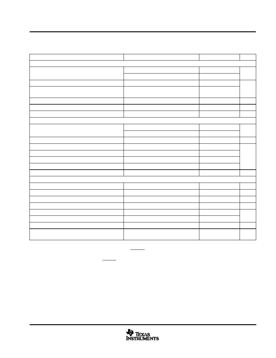
ABSOLUTE MAXIMUM RATINGS
over operating free-air temperature range unless otherwise noted(1)(3)
UNIT
Supply voltage(2), VCC
11
V
Supply current, ICC
20
mA
Output peak current, OUT1, OUT2, 5% duty cycle
±
1
A
Output energy, OUT1, OUT2, capacitive load
20
µ
J
Analog inputs, FB1, FB2, CS1, CS2, SYNC
≠0.3 to 6.3
V
Operating junction temperature, TJ
150
_
C
Storage temperature range, Tstg
≠65 to 150
_
C
Lead temperature (soldering, 10 sec)
300
_
C
(1)
Currents are positive into, negative out of the specified terminal. All voltages are with respect to GND.
(2)
In normal operation, VCC is powered through a current-limiting resistor. Absolute maximum of 11 V applies when driven from a low impedance
such that the VCC current does not exceed 20 mA.
(3)
Stresses beyond those listed under "absolute maximum ratings" may cause permanent damage to the device. These are stress ratings only,
and functional operation of the device at these or any other conditions beyond those indicated under "recommended operating conditions"
is not implied. Exposure to absolute-maximum-rated conditions for extended periods may affect device reliability.
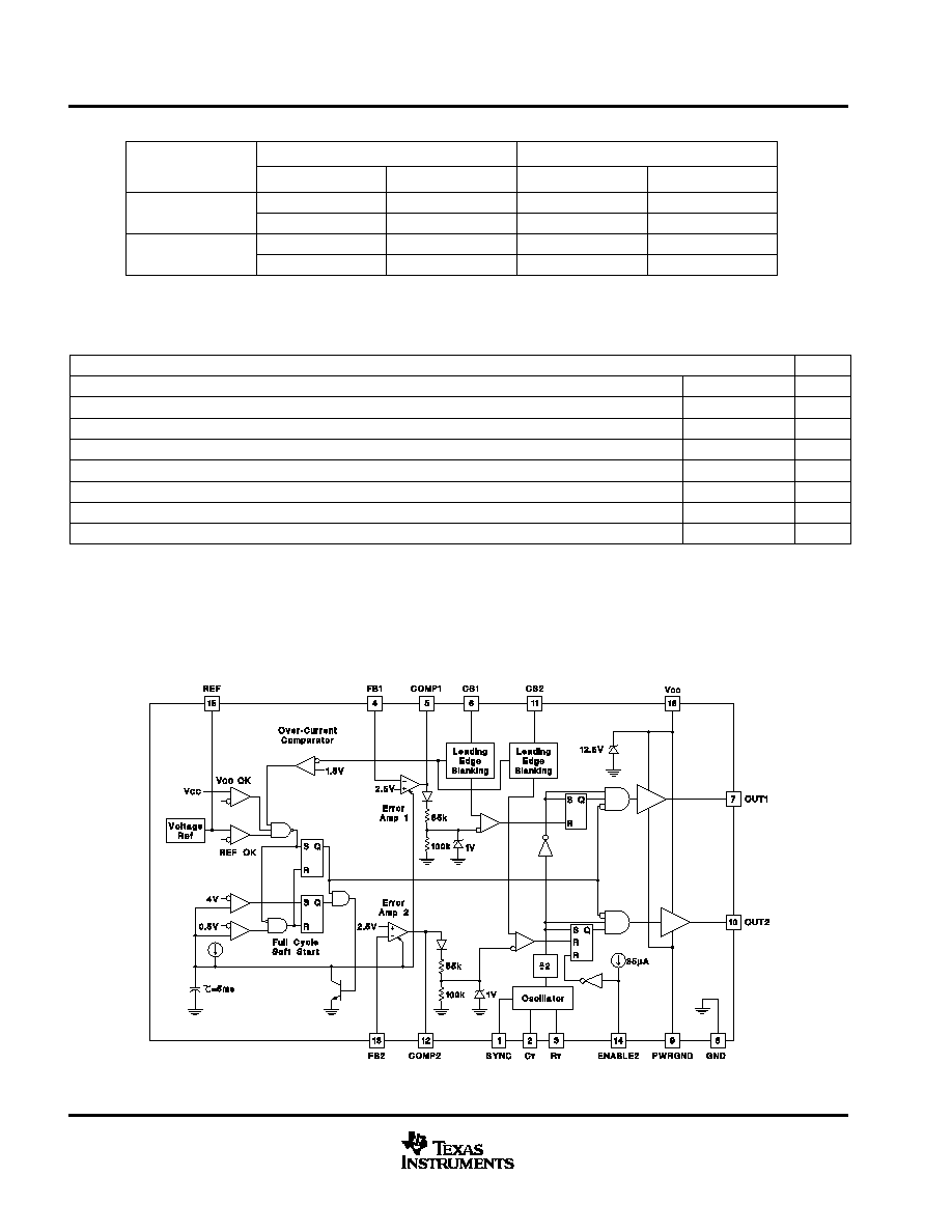
BLOCK DIAGRAM
UDG≠92062≠1
UCC2810, UCC2811
UCC3810, UCC3811
SLUS162A ≠ FEBRUARY 1999 ≠ REVISED OCTOBER 2002
3
www.ti.com
ELECTRICAL CHARACTERISTICS
All parameters are the same for both channels, ≠40
_
C
T
A
85
_
C for the UCC281x, 0
_
C
T
A
70
_
C for the
UCC381x, V
CC
= 10 V
(1)
; R
T
= 150 k
, C
T
= 120 pF; no load; T
A
= T
J
; (unless otherwise specified)
PARAMETER
TEST CONDITIONS
MIN
TYP
MAX
UNIT
REFERENCE
V
Output voltage
TJ = 25
_
C
4.925
5.000
5.075
V
VCC Output voltage
TJ = full range,
0 mA
IREF
5 mA
4.85
5.00
5.10
V
Load regulation
0 mA
IREF
5 mA
5
25
Line regulation
UVLO stop threshold voltage,
0.5 V
VCC
VSHUNT
12
mV
Output noise voltage(7)
10 Hz < f < 10 kHz,
TJ = 25
_
C
235
µ
V
Long term stability(7)
TA = 125
_
C, 1000
hours
5
mV
IO(SC)Output short circuit current
≠8
≠25
mA
OSCILLATOR
f
Oscillator frequency(2)
RT = 30 k
CT = 120 pF
860
980
1100
kHz
fOSC Oscillator frequency(2)
RT = 150 k
CT = 120 pF
190
220
250
kHz
Temperature stability(7)
2.5%
Peak voltage
2.5
Valley voltage
0.05
V
Peak-to-peak amplitude
2.25
2.45
2.65
V
SYNC threshold voltage
0.80
1.65
2.20
SYNC input current
SYNC = 5 V
30
µ
A
ERROR AMPLIFIER
VFB FB input voltage
COMP = 2.5 V
2.44
2.50
2.56
V
IFB
FB input bias current
±
1
µ
A
Open loop voltage gain
60
73
dB
fGAIN Unity gain bandwidth(7)
2
MHz
ISINK Sink current, COMP
FB = 2.7 V,
COMP = 1 V
0.3
1.4
3.5
mA
ISRCESource current, COMP
FB = 1.8 V,
COMP = 4 V
≠0.2
≠0.5
≠0.8
mA
Minimum duty cycle
COMP = 0 V
0%
Soft-start rise time, COMP
FB = 1.8 V,
rise from 0.5 V to (REF ≠ 1.5 V)
5
ms
(1) For UCC3810, adjust VCC above the start threshold before setting at 10 V.
(2) Oscillator frequency is twice the output frequency. f
OSC
+
4
R
T
C
T
(3) Current sense gain A is defined by: A
+
D
V
COMP
D
V
CS
, 0 V
VCS
0.8 V.
(4) Parameter measured at trip point of latch with FB = 0 V.
(5) CS blank time is measured as the difference between the minimum non-zero on-time and the CS-to-OUT delay.
(6) Start threshold voltage and VCC internal zener voltage track each other.
(7) Ensured by design. Not production tested.
UCC2810, UCC2811
UCC3810, UCC3811
SLUS162A ≠ FEBRUARY 1999 ≠ REVISED OCTOBER 2002
4
www.ti.com
ELECTRICAL CHARACTERISTICS
≠40
_
C
T
A
85
_
C for the UCC281X, 0
_
C
T
A
70
_
C for the UCC381X, V
CC
= 10 V
(1)
; R
T
= 150 k
, C
T
= 120 pF;
no load; T
A
= T
J
; all parameters are the same for both channels (unless otherwise specified)
PARAMETER
TEST CONDITIONS
MIN
TYP
MAX
UNIT
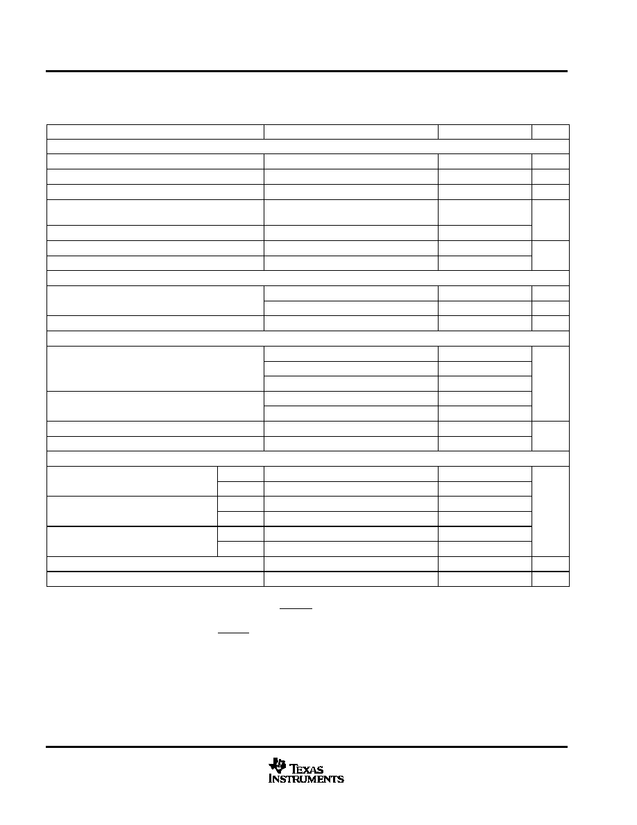
CURRENT SENSE
Gain(3)
1.20
1.55
1.80
V/V
Maximum input signal(4)
COMP = 5 V
0.9
1.0
1.1
V
ICS
Input bias current, CS
±
200
nA
Propagation delay time (CS to OUT)
CS steps from 0 V to 1.2 V,
COMP = 2.5 V
75
ns
Blank time, CS(5)
55
ns
Overcurrent threshold voltage, CS
1.35
1.55
1.85
V
COMP-to-CS offset voltage
CS = 0 V
0.45
0.90
1.35
V
PWM
Maximum duty cycle(7)
RT = 150 k
,
CT = 120 pF
45%
49%
50%
Maximum duty cycle(7)
RT = 30 k
,
CT = 120 pF
40%
45%
48%
Minimum on-time
CS = 1.2 V,
COMP = 5 V
130
ns
OUTPUT
IOUT = 20 mA
0.12
0.42
VOL Low-level output voltage
IOUT = 200 mA
0.48
1.10
VOL Low level out ut voltage
IOUT = 20 mA,
VCC = 0 V
0.7
1.2
V
V
High level output voltage (V
OUT)
IOUT = ≠20 mA
0.15
0.42
V
VOH High-level output voltage (VCC ≠ OUT)
IOUT = ≠200 mA
1.2
2.3
tR
Rise time, OUT
COUT = 1 nF
20
50
ns
tF
Fall time, OUT
COUT = 1 nF
30
60
ns
UNDERVOLTAGE LOCKOUT (UVLO)
Start threshold voltage
UCCx810
9.6
11.3
13.2
Start threshold voltage
UCCx811
7.4
8.4
9.4
Stop threshold oltage
UCCx810
7.1
8.3
9.5
V
Stop threshold voltage
UCCx811
6
7
8
V
Start to stop hysteresis
UCCx810
1.7
3.0
4.7
Start-to-stop hysteresis
UCCx811
0.65
1.40
2.15
ENABLE2 input bias current
ENABLE2 = 0 V
≠20
≠35
≠55
µ
A
ENABLE2 input threshold voltage
0.80
1.53
2.00
V
(1) For UCC3810, adjust VCC above the start threshold before setting at 10 V.
(2) Oscillator frequency is twice the output frequency. f
OSC
+
4
R
T
C
T
(3) Current sense gain A, is defined by: A
+
D
V
COMP
D
V
CS
, 0 V
VCS
0.8 V.
(4) Parameter measured at trip point of latch with FB = 0 V.
(5) CS blank time is measured as the difference between the minimum non-zero on-time and the CS-to-OUT delay.
(6) Start threshold voltage and VCC internal zener voltage track each other.
(7) Ensured by design. Not production tested.
UCC2810, UCC2811
UCC3810, UCC3811
SLUS162A ≠ FEBRUARY 1999 ≠ REVISED OCTOBER 2002
5
www.ti.com
ELECTRICAL CHARACTERISTICS
All parameters are the same for both channels, ≠40
_
C
T
A
85
_
C for the UCC281x, 0
_
C
T
A
70
_
C for the
UCC381x, V
CC
= 10 V
(1)
; R
T
= 150 k
, C
T
= 120 pF; no load; T
A
= T
J
; (unless otherwise specified)
PARAMETER
TEST CONDITIONS
MIN
TYP
MAX
UNIT
OVERALL
Startup current
VCC < Start threshold voltage
0.15
0.25
Operating supply current, outputs off
VCC = 10 V,
FB = 2.75 V
2
3
Operating supply current outputs on
VCC = 10 V,
FB = 0 V,
CS = 0 V,
RT = 150 k
3.2
5.1
mA
Operating supply current, outputs on
VCC = 10 V,
FB = 0 V,
CS = 0 V,
RT = 30 k
8.5
14.5
VCC internal zener voltage(6)
ICC = 10 mA
11.0
12.9
14.0
VCC internal zener voltage minus start
threshold voltage
0.4
1.2
V
(6) Start threshold voltage and VCC internal zener voltage track each other.
Terminal Functions
TERMINAL
I/O
DESCRIPTION
NAME
NO.
I/O
DESCRIPTION
COMP1
5
O
Lo
impedance o tp t of the error amplifiers
COMP2
12
O
Low impedance output of the error amplifiers.
CS1
6
I
Current sense inputs to the PWM comparators. These inputs have leading edge blanking. For most
applications, no input filtering is required. Leading edge blanking disconnects the CS inputs from all
internal circuits for the first 55 ns of each PWM cycle When used with very slow diodes or in other
CS2
11
I
internal circuits for the first 55 ns of each PWM cycle. When used with very slow diodes or in other
applications where the current sense signal is unusually noisy, a small current-sense R-C filter may
be required.
CT
2
O
The timing capacitor of the oscillator. Recommended values of CT are between 100 pF and 1 nF.
Connect the timing capacitor directly across CT and GND.
ENABLE2
14
I
A logic input which disables PWM 2 when low. This input has no effect on PWM 1. This input is inter-
nally pulled high. In most applications it can be left floating. In unusually noisy applications, the input
should be bypassed with a 1-nF ceramic capacitor. This input has TTL compatible thresholds.
FB1
4
I
The high impedance inverting inputs of the error amplifiers
FB2
13
I
The high impedance inverting inputs of the error amplifiers.
GND
8
≠
To separate noise from the critical control circuits, this part has two different ground connections:
GND and PWRGND. GND and PWRGND must be electrically connected together. However, use
care to avoid coupling noise into GND.
OUT1
7
O
The high-current push-pull outputs of the PWM are intended to drive power MOSFET gates through
a small resistor This resistor acts as both a current limiting resistor and as a damping impedance to
OUT2
10
O
a small resistor. This resistor acts as both a current limiting resistor and as a damping impedance to
minimize ringing and overshoot.
PWRGND
9
≠
To separate noise from the critical control circuits, this part has two different ground connections:
GND and PWRGND. GND and PWRGND must be electrically connected together.
REF
15
O
The output of the 5-V reference. Bypass REF to GND with a ceramic capacitor
0.01-
µ
F for best
performance.
RT
3
O
The oscillator charging current is set by the value of the resistor connected from RT to GND. This pin
is regulated to 1 V, but the actual charging current is 10 V/RT. Recommended values of RT are be-
tween 10 k
and 470 k
. For a given frequency, higher timing resistors give higher maximum duty
cycle and slightly lower overall power consumption.
SYNC
1
I
This logic input can be used to synchronize the oscillator to a free running oscillator in another part.
This pin is edge triggered with TTL thresholds, and requires at least a 10-ns-wide pulse. If unused,
this pin can be grounded, open circuited, or connected to REF.
VCC
16
I
The power input to the device. This pin supplies current to all functions including the high current
output stages and the precision reference. Therefore, it is critical that VCC be directly bypassed to
PWRGND with an 0.1-
µ
F ceramic capacitor.
UCC2810, UCC2811
UCC3810, UCC3811
SLUS162A ≠ FEBRUARY 1999 ≠ REVISED OCTOBER 2002
6
www.ti.com
APPLICATION INFORMATION
timing resistor
Supply current decreases with increased R
T
by the relationship:
D
I
CC
+
11 V
R
T
For more information, see the detailed oscillator block diagram.
leading edge blanking and current sense
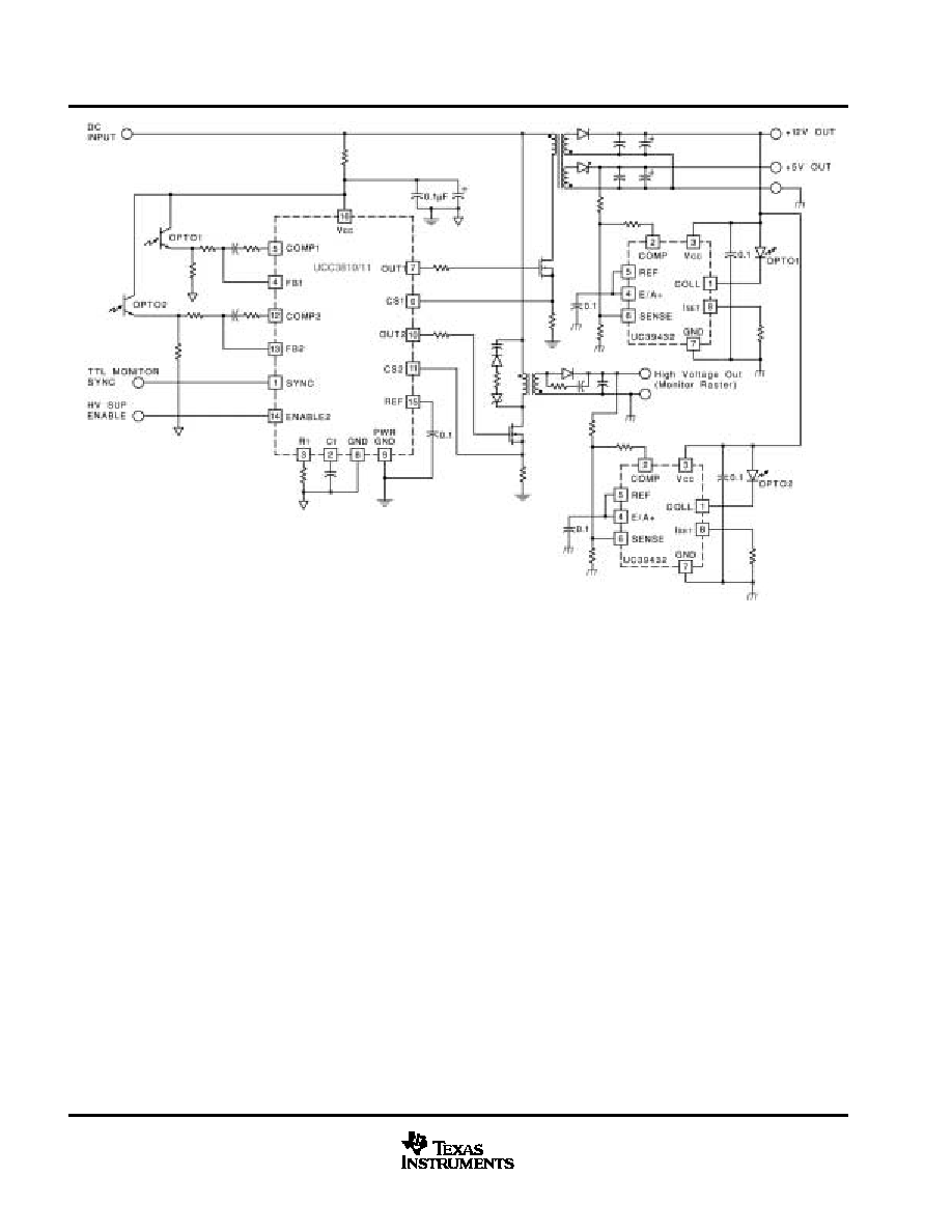
Figure 1 shows how an external power stage is connected to the UCC3810/UCC3811. The gate of an external
power N-channel MOSFET is connected to OUT through a small current-limiting resistor. For most applications,
a 10-
resistor is adequate to limit peak current and also practical at damping resonances between the gate
driver and the MOSFET input reactance. Long gate lead length increases gate capacitance and mandates a
higher series gate resistor to damp the R-L-C tank formed by the lead, the MOSFET input reactance, and the
device's driver output resistance.
The UCC3810/UCC3811 features internal leading edge blanking of the current-sense signal on both current
sense inputs. The blank time starts when OUT rises and continues for 55 ns. During that 55 ns period, the signal
on CS is ignored. For most PWM applications, this means that the CS input can be connected to the
current-sense resistor as shown in Figure 1. However, high speed grounding practices and short lead lengths
are still required for good performance.
Figure 1. Detailed Block Diagram
oscillator
The UCC3810/UCC3811 oscillator generates a sawtooth wave at CT. The sawtooth rise time is set by the
resistor from RT to GND. Since R
T
is biased at 1 V, the current through R
T
is 1 V/R
T
. The actual charging current
is 10 times higher. The fall time is set by an internal transistor on-resistance of approximately 100
. During the
fall time, all outputs are off and the maximum duty cycle is reduced to below 50%. Larger timing capacitors
increase the discharge time and reduce frequency. However, the percentage maximum duty cycle is only a
function of the timing resistor R
T
, and the internal 100-
discharge resistance.
(1)

UCC2810, UCC2811
UCC3810, UCC3811
SLUS162A ≠ FEBRUARY 1999 ≠ REVISED OCTOBER 2002
7
www.ti.com
APPLICATION INFORMATION
error amplifier output stage
The UCC3810 and UCC3811 error amplifiers are operational amplifiers with low-output resistance and
high-input resistance. The output stage of one error amplifier is shown in Figure 3. This output stage allows the
error amplifier output to swing close to GND and as high as one diode drop below 5 V with little loss in amplifier
performance.
Figure 2. Oscillator
Figure 3. Error Amplifier Output Stage
UCC2810, UCC2811
UCC3810, UCC3811
SLUS162A ≠ FEBRUARY 1999 ≠ REVISED OCTOBER 2002
8
www.ti.com
TYPICAL CHARACTERISTICS
Figure 4
ERROR AMPLIFIER GAIN AND PHASE
vs
FREQUENCY
Figure 5
OSCILLATOR FREQUENCY
vs
TIMING RESISTANCE
Figure 6
OSCILLATOR FREQUENCY
vs
TEMPERATURE
Figure 7
MAXIMUM DUTY CYCLE
vs
TIMING RESISTANCE
UCC2810, UCC2811
UCC3810, UCC3811
SLUS162A ≠ FEBRUARY 1999 ≠ REVISED OCTOBER 2002
9
www.ti.com
TYPICAL CHARACTERISTICS
Figure 8
INPUT CURRENT
vs
OSCILLATOR FREQUENCY
Figure 9
MAXIMUM DUTY CYCLE
vs
FREQUENCY
UCC2810, UCC2811
UCC3810, UCC3811
SLUS162A ≠ FEBRUARY 1999 ≠ REVISED OCTOBER 2002
10
www.ti.com
UDG≠94022
Figure 10. Typical Application

UCC2810, UCC2811
UCC3810, UCC3811
SLUS162A ≠ FEBRUARY 1999 ≠ REVISED OCTOBER 2002
11
www.ti.com
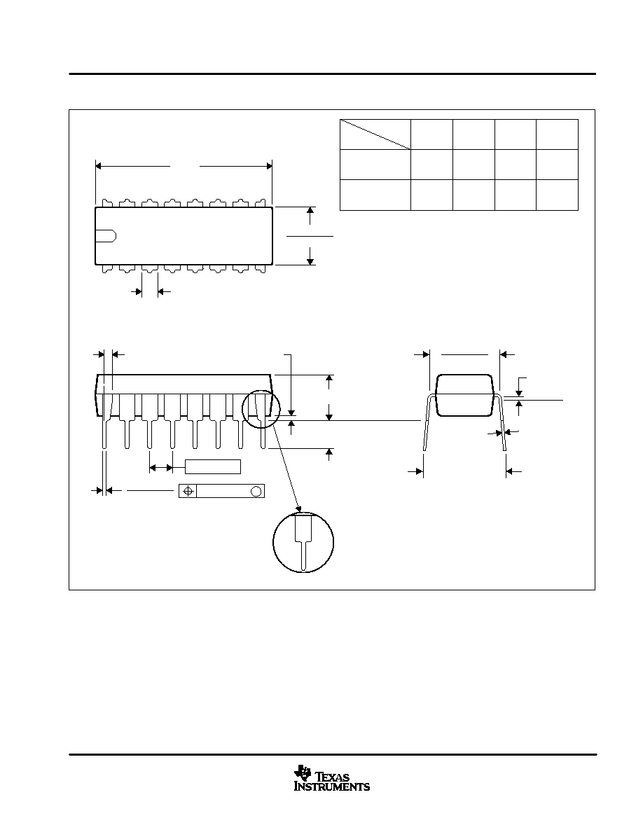
DW (R-PDSO-G**)
PLASTIC SMALL-OUTLINE PACKAGE
16 PINS SHOWN
4040000/E 08/01
Seating Plane
0.400 (10,15)
0.419 (10,65)
0.104 (2,65) MAX
1
0.012 (0,30)
0.004 (0,10)
A
8
16
0.020 (0,51)
0.014 (0,35)
0.291 (7,39)
0.299 (7,59)
9
0.010 (0,25)
0.050 (1,27)
0.016 (0,40)
(15,24)
(15,49)
PINS **
0.010 (0,25) NOM
A MAX
DIM
A MIN
Gage Plane
20
0.500
(12,70)
(12,95)
0.510
(10,16)
(10,41)
0.400
0.410
16
0.600
24
0.610
(17,78)
28
0.700
(18,03)
0.710
0.004 (0,10)
M
0.010 (0,25)
0.050 (1,27)
0
∞
≠8
∞
(11,51)
(11,73)
0.453
0.462
18
NOTES: A. All linear dimensions are in inches (millimeters).
B. This drawing is subject to change without notice.
C. Body dimensions do not include mold flash or protrusion not to exceed 0.006 (0,15).
D. Falls within JEDEC MS-013

UCC2810, UCC2811
UCC3810, UCC3811
SLUS162A ≠ FEBRUARY 1999 ≠ REVISED OCTOBER 2002
12
www.ti.com
J (R-GDIP-T**)
CERAMIC DUAL-IN-LINE
1
20
0.290
(7,87)
0.310
0.975
(24,77)
(23,62)
0.930
(7,37)
0.245
(6,22)
(7,62)
0.300
16
14
PINS **
0.290
(7,87)
0.310
0.785
(19,94)
(19,18)
0.755
(7,37)
0.310
(7,87)
(7,37)
0.290
0.755
(19,18)
(19,94)
0.785
0.245
(6,22)
(7,62)
0.300
A
0.300
(7,62)
(6,22)
0.245
A MIN
A MAX
B MAX
B MIN
C MIN
C MAX
DIM
0
∞
≠15
∞
Seating Plane
0.014 (0,36)
0.008 (0,20)
4040083/E 03/99
C
8
7
0.020 (0,51) MIN
B
0.070 (1,78)
0.100 (2,54)
0.065 (1,65)
0.045 (1,14)
14 LEADS SHOWN
14
0.015 (0,38)
0.023 (0,58)
0.100 (2,54)
0.200 (5,08) MAX
0.130 (3,30) MIN
NOTES: A. All linear dimensions are in inches (millimeters).
B. This drawing is subject to change without notice.
C. This package is hermetically sealed with a ceramic lid using glass frit.
D. Index point is provided on cap for terminal identification.
E. Falls within MIL STD 1835 GDIP1-T14, GDIP1-T16, and GDIP1-T20
UCC2810, UCC2811
UCC3810, UCC3811
SLUS162A ≠ FEBRUARY 1999 ≠ REVISED OCTOBER 2002
13
www.ti.com
N (R-PDIP-T**)
PLASTIC DUAL-IN-LINE PACKAGE
0.325 (8,26)
0.300 (7,62)
0.010 (0,25) NOM
Gauge Plane
0.015 (0,38)
0.430 (10,92) MAX
20
0.975
(24,77)
0.940
(23,88)
18
0.920
0.850
14
0.775
0.745
(19,69)
(18,92)
16
0.775
(19,69)
(18,92)
0.745
A MIN
DIM
A MAX
PINS **
(23,37)
(21,59)
Seating Plane
14/18 PIN ONLY
4040049/D 02/00
9
8
0.070 (1,78) MAX
A
0.035 (0,89) MAX
0.020 (0,51) MIN
16
1
0.015 (0,38)
0.021 (0,53)
0.200 (5,08) MAX
0.125 (3,18) MIN
0.240 (6,10)
0.260 (6,60)
M
0.010 (0,25)
0.100 (2,54)
16 PINS SHOWN
NOTES: A. All linear dimensions are in inches (millimeters).
B. This drawing is subject to change without notice.
C. Falls within JEDEC MS-001 (20-pin package is shorter than MS-001).

IMPORTANT NOTICE
Texas Instruments Incorporated and its subsidiaries (TI) reserve the right to make corrections, modifications,
enhancements, improvements, and other changes to its products and services at any time and to discontinue
any product or service without notice. Customers should obtain the latest relevant information before placing
orders and should verify that such information is current and complete. All products are sold subject to TI's terms
and conditions of sale supplied at the time of order acknowledgment.
TI warrants performance of its hardware products to the specifications applicable at the time of sale in
accordance with TI's standard warranty. Testing and other quality control techniques are used to the extent TI
deems necessary to support this warranty. Except where mandated by government requirements, testing of all
parameters of each product is not necessarily performed.
TI assumes no liability for applications assistance or customer product design. Customers are responsible for
their products and applications using TI components. To minimize the risks associated with customer products
and applications, customers should provide adequate design and operating safeguards.
TI does not warrant or represent that any license, either express or implied, is granted under any TI patent right,
copyright, mask work right, or other TI intellectual property right relating to any combination, machine, or process
in which TI products or services are used. Information published by TI regarding third≠party products or services
does not constitute a license from TI to use such products or services or a warranty or endorsement thereof.
Use of such information may require a license from a third party under the patents or other intellectual property
of the third party, or a license from TI under the patents or other intellectual property of TI.
Reproduction of information in TI data books or data sheets is permissible only if reproduction is without
alteration and is accompanied by all associated warranties, conditions, limitations, and notices. Reproduction
of this information with alteration is an unfair and deceptive business practice. TI is not responsible or liable for
such altered documentation.
Resale of TI products or services with statements different from or beyond the parameters stated by TI for that
product or service voids all express and any implied warranties for the associated TI product or service and
is an unfair and deceptive business practice. TI is not responsible or liable for any such statements.
Mailing Address:
Texas Instruments
Post Office Box 655303
Dallas, Texas 75265
Copyright
2002, Texas Instruments Incorporated