
UCC2813 0/ 1/ 2/ 3/ 4/ 5 Q1
LOW POWER BICMOS CURRENT MODE PWM
SGLS245 - MAY 2004
1
POST OFFICE BOX 655303
∑
DALLAS, TEXAS 75265
D
Qualification in Accordance With
AEC-Q100
D
Qualified for Automotive Applications
D
Customer-Specific Configuration Control
Can Be Supported Along With
Major-Change Approval
D
ESD Protection Exceeds 200 V Using
Machine Model (C = 200 pF, R = 0)
D
100
µ
A Typical Starting Supply Current
D
500
µ
A Typical Operating Supply Current
Contact Texas Instruments for details. Q100 qualification data
available on request.
D
Operation to 1 MHz
D
Internal Soft Start
D
Internal Fault Soft Start
D
Internal Leading-Edge Blanking of the
Current Sense Signal
D
1-A Totem-Pole Output
D
70 ns Typical Response from
Current-Sense to Gate Drive Output
D
1.5% Tolerance Voltage Reference
D
Same Pinout as UC3802, UC3842, and
UC3842A
description
The UCC2813-0/-1/-2/-3/-4/-5 family of high-speed, low-power integrated circuits contain all of the control and
drive components required for off-line and dc-to-dc fixed frequency current-mode switching power supplies with
minimal parts count.
These devices have the same pin configuration as the UC2842/3/4/5 family and also offer the added features
of internal full-cycle soft start and internal leading-edge blanking of the current-sense input.
The UCC2813-0/-1/-2/-3/-4/-5 family offers choice of maximum duty cycle and critical voltage levels. Lower
reference parts such as the UCC2813-3 and UCC2813-5 fit best into battery operated systems, while the higher
reference and the higher UVLO hysteresis of the UCC2813-2 and UCC2813-4 make these ideal choices for use
in off-line power supplies.
The UCC2813-xQ-Q1 series is specified for the automotive temperature range of -40
_
C to 125
_
C and qualified
in accordance with AEC-Q100 stress test qualification for integrated circuits.
PART NUMBER
MAXIMUM DUTY CYCLE
REFERENCE VOLTAGE
TURN-ON THRESHOLD
TURN-OFF THRESHOLD
UCC2813-0
100%
5 V
7.2 V
6.9 V
UCC2813-1
50%
5 V
9.4 V
7.4 V
UCC2813-2
100%
5 V
12.5 V
8.3 V
UCC2813-3
100%
4 V
4.1 V
3.6 V
UCC2813-4
50%
5 V
12.5 V
8.3 V
UCC2813-5
50%
4 V
4.1 V
3.6 V
Copyright
2004 Texas Instruments Incorporated
PRODUCTION DATA information is current as of publication date.
Products conform to specifications per the terms of Texas Instruments
standard warranty. Production processing does not necessarily include
testing of all parameters.
Please be aware that an important notice concerning availability, standard warranty, and use in critical applications of
Texas Instruments semiconductor products and disclaimers thereto appears at the end of this data sheet.

UCC2813 0/ 1/ 2/ 3/ 4/ 5 Q1
LOW POWER BICMOS CURRENT MODE PWM
SGLS245 - MAY 2004
2
POST OFFICE BOX 655303
∑
DALLAS, TEXAS 75265
block diagram
-
-
-
AVAILABLE OPTIONS
TA
SOIC-8
SMALL OUTLINE (D)
UCC2813-0QDRQ1
UCC2813-1QDRQ1
-40
_
C to 125
_
C
UCC2813-2QDRQ1
-40
_
C to 125
_
C
UCC2813-3QDRQ1
UCC2813-4QDRQ1
UCC2813-5QDRQ1
The UCC2813-x-Q1 is only available taped
and reeled in quantities of 2500 devices per
reel.
1
2
3
4
8
7
6
5
COMP
FB
CS
RC
REF
V
CC
OUT
GND
D PACKAGE
(TOP VIEW)
UCC2813 0/ 1/ 2/ 3/ 4/ 5 Q1
LOW POWER BICMOS CURRENT MODE PWM
SGLS245 - MAY 2004
3
POST OFFICE BOX 655303
∑
DALLAS, TEXAS 75265
Ordering Information
UCC 2
0
Q
PACKAGE
D = Plastic SOIC
PRODUCT OPTION
0 through 5
AUTOMOTIVE TEMPERATURE RANGE INDICATOR
D
TAPE and REEL INDICATOR
R
813-
Q1
Q100 INDICATOR
absolute maximum ratings over operating free-air temperature range (unless otherwise noted)
V
CC
voltage
w
12 V
. . . . . . . . . . . . . . . . . . . . . . . . . . . . . . . . . . . . . . . . . . . . . . . . . . . . . . . . . . . . . . . . . . . . . . . . . . . . .
V
CC
current
w
30 mA
. . . . . . . . . . . . . . . . . . . . . . . . . . . . . . . . . . . . . . . . . . . . . . . . . . . . . . . . . . . . . . . . . . . . . . . . . . .
Output current, I
O
±
1 A
. . . . . . . . . . . . . . . . . . . . . . . . . . . . . . . . . . . . . . . . . . . . . . . . . . . . . . . . . . . . . . . . . . . . . . . . .
Output energy, (Capacitive Load)
20
µ
J
. . . . . . . . . . . . . . . . . . . . . . . . . . . . . . . . . . . . . . . . . . . . . . . . . . . . . . . . . . .
Analog Inputs (FB, CS)
-0.3 V to 6.3 V
. . . . . . . . . . . . . . . . . . . . . . . . . . . . . . . . . . . . . . . . . . . . . . . . . . . . . . . . . . . .
Power Dissipation at T
A
< +25
_
C (D package)
0.65 W
. . . . . . . . . . . . . . . . . . . . . . . . . . . . . . . . . . . . . . . . . . . . . . .
Storage temperature range, T
stg
-65
_
C to 150
_
C
. . . . . . . . . . . . . . . . . . . . . . . . . . . . . . . . . . . . . . . . . . . . . . . . . . . .
Lead temperature soldering 1,6 mm (1/16 inch) from case for 10 seconds
300
_
C
. . . . . . . . . . . . . . . . . . . . . . .
Stresses beyond those listed under "absolute maximum ratings" may cause permanent damage to the device. These are stress ratings only, and
functional operation of the device at these or any other conditions beyond those indicated under "recommended operating conditions" is not
implied. Exposure to absolute-maximum-rated conditions for extended periods may affect device reliability.
Unless otherwise indicated, voltages are reference to ground and currents are positive into and negative out of the specified terminals.
w
In normal operation VCC is powered through a current limiting resistor. Absolute maximum of 12 V applies when VCC is driven from a low
impedance source such that ICC does not exceed 30 mA (which includes gate drive current requirement).
electrical characteristics T
A
= -40
_
C to 125
_
C, V
CC
= 10 V (see Note 1), RT = 100 k
from REF to
RC, CT = 330 pF from RC to GND, 0.1-F capacitor from V
CC
to GND, 0.1-F capacitor from V
REF
to
GND and T
A
= T
J
(unless otherwise stated)
PARAMETER
TEST CONDITIONS
MIN
TYP
MAX
UNITS
Reference Section
Output voltage
TJ = 25
_
C, I = 0.2 mA
UCC2813-0/1/2/4
4.925
5
5.075
V
Output voltage
TJ = 25
_
C, I = 0.2 mA
UCC2813-3/5
3.94
4
4.06
V
Load regulation voltage
I = 0.2 mA to 5 mA
10
30
mV
Total variation voltage
See Note 5
UCC2813-0/1/2/4
4.84
5
5.1
V
Total variation voltage
See Note 5
UCC2813-3/5
3.84
4
4.08
V
Output noise voltage
f = 10 Hz to 10 kHz,
See Note 7
TJ = 25
_
C
70
µ
V
Long term stability
1000 hours,
See Note 7
TA = 125
_
C
5
mV
Output short-circuit current
-5
-35
mA

UCC2813 0/ 1/ 2/ 3/ 4/ 5 Q1
LOW POWER BICMOS CURRENT MODE PWM
SGLS245 - MAY 2004
4
POST OFFICE BOX 655303
∑
DALLAS, TEXAS 75265
electrical characteristics T
A
= -40
_
C to 125
_
C, V
CC
= 10 V (see Note 1), RT = 100 k
from REF to
RC, CT = 330 pF from RC to GND, 0.1 F capacitor from V
CC
to GND, 0.1 F capacitor from V
REF
to GND
and T
A
= T
J
(unless otherwise stated)
PARAMETER
TEST CONDITIONS
MIN
TYP
MAX
UNITS
Oscillator Section
Oscillator frequency
See Note 2
UCC2813-0/1/2/4
40
46
52
kHz
Oscillator frequency
See Note 2
UCC2813-3/5
26
31
36
kHz
Temperature stability
See Note 7
2.5
%
Amplitude peak-to-peak
2.25
2.4
2.55
V
Oscillator peak voltage
2.45
V
Error Amplifier Section
Input voltage
COMP = 2.5 V
UCC2813-0/1/2/4
2.42
2.5
2.56
V
Input voltage
COMP = 2.0 V
UCC2813-3/5
1.92
2
2.05
V
Input bias current
-2
2
µ
A
Open loop voltage gain
60
80
dB
COMP sink current
FB = 2.7 V,
COMP = 1.1 V
0.3
3.5
mA
COMP source current
FB = 1.8 V,
COMP = REF - 1.2 V
-0.2
-0.5
-0.8
mA
Gain bandwidth product
See Note 7
2
MHz
PWM Section
Maximum duty cycle
UCC2813-0/2/3
97
99
100
%
Maximum duty cycle
UCC2813-1/4/5
48
49
50
%
Minimum duty cycle
COMP = 0 V
0
%
Current Sense Section
Gain
See Note 3
1.1
1.65
1.8
V/V
Maximum input signal
COMP = 5 V,
See Note 4
0.9
1
1.1
V
Input bias current
-200
200
nA
CS blank time
50
100
150
ns
Over-current threshold voltage
1.32
1.55
1.7
V
COMP to CS offset voltage
CS = 0 V
0.45
0.9
1.35
V
Output Section (OUT)
IOUT = 20 mA
All parts
0.1
0.4
Low-level output voltage
IOUT = 200 mA
All parts
0.35
0.9
V
Low-level output voltage
IOUT = 50 mA, VCC = 5 V
UCC2813-3/5
0.15
0.4
V
IOUT = 20 mA, VCC = 0 V
All parts
0.7
1.2
IOUT = -20 mA
All parts
0.15
0.4
High-level output voltage VSAT (VCC - OUT)
IOUT = -200 mA
All parts
1
1.9
V
High-level output voltage VSAT (VCC - OUT)
IOUT = -50 mA, VCC = 5 V
UCC2813-3/5
0.4
0.9
V
Rise time
CL = 1 nF
41
70
ns
Fall time
CL = 1 nF
44
75
ns

UCC2813 0/ 1/ 2/ 3/ 4/ 5 Q1
LOW POWER BICMOS CURRENT MODE PWM
SGLS245 - MAY 2004
5
POST OFFICE BOX 655303
∑
DALLAS, TEXAS 75265
electrical characteristics T
A
= -40
_
C to 125
_
C, V
CC
= 10 V (see Note 1), RT = 100 k
from REF to
RC, CT = 330 pF from RC to GND, 0.1 F capacitor from V
CC
to GND, 0.1 F capacitor from V
REF
to GND
and T
A
= T
J
(unless otherwise stated)
PARAMETER
TEST CONDITIONS
MIN
TYP
MAX
UNITS
Undervoltage Lockout Section
UCC2813-0
6.6
7.2
7.8
Start threshold
See Note 6
UCC2813-1
8.6
9.4
10.2
V
Start threshold
See Note 6
UCC2813-2/4
11.5
12.5
13.5
V
UCC2813-3/5
3.7
4.1
4.5
UCC2813-0
6.3
6.9
7.5
Stop threshold
See Note 6
UCC2813-1
6.8
7.4
8
V
Stop threshold
See Note 6
UCC2813-2/4
7.6
8.3
9
V
UCC2813-3/5
3.2
3.6
4
UCC2813-0
0.12
0.3
0.48
Start to stop hysteresis
UCC2813-1
1.6
2
2.4
V
Start to stop hysteresis
UCC2813-2/4
3.5
4.2
5.1
V
UCC2813-3/5
0.2
0.5
0.8
Soft Start Section
COMP rise time
FB = 1.8 V,
Rise from 0.5 V to REF - 1 V
4
10
ms
Overall Section
Start-up current
VCC < Start Threshold
0.1
0.23
mA
Operating supply current
FB = 0 V,
CS = 0 V,
RC = 0 V
0.5
1.2
mA
VCC internal zener voltage
ICC = 10 mA,
See Notes 6 and 8
12
13.5
15
V
VCC internal zener voltage minus start
threshold voltage
See Note 6
UCC2813-2/4
0.5
1.0
V
NOTES:
1. Adjust VCC above the start threshold before setting at 10 V.
2. Oscillator frequency for the UCC2813-0, UCC2813-2, and UCC2813-3 is the output frequency.
Oscillator frequency for the UCC2813-1, UCC2813-4, and UCC2813-5 is twice the output frequency.
3. Gain is defined by:
A =
D
VCOMP
D
VCS
0
v
VCS
v
0.8 V.
4. Parameter measured at trip point of latch with pin 2 at 0 V.
5. Total variation includes temperature stability and load regulation.
6. Start threshold, stop threshold, and Zener shunt thresholds track one another.
7. Not production tested.
8. The device is fully operating in clamp mode as the forcing current is higher than the normal operating supply current.

UCC2813 0/ 1/ 2/ 3/ 4/ 5 Q1
LOW POWER BICMOS CURRENT MODE PWM
SGLS245 - MAY 2004
6
POST OFFICE BOX 655303
∑
DALLAS, TEXAS 75265
detailed terminal descriptions
COMP
COMP is the output of the error amplifier and the input of the PWM comparator.
Unlike other devices, the error amplifier in the UCC2813 family is a true, low output-impedance, 2-MHz
operational amplifier. As such, the COMP terminal can both source and sink current. However, the error
amplifier is internally current limited, so that one can command zero duty cycle by externally forcing COMP to
GND.
The UCC2813 family features built-in full cycle soft start. Soft start is implemented as a clamp on the maximum
COMP voltage.
CS
CS is the input to the current sense comparators. The UCC2813 family has two different current sense
comparators: the PWM comparator and an overcurrent comparator.
The UCC2813 family contains digital current sense filtering, which disconnects the CS terminal from the current
sense comparator during the 100 ns interval immediately following the rising edge of the OUT pin. This digital
filtering, also called leading-edge blanking, means that in most applications, no analog filtering (RC filter) is
required on CS. Compared to an external RC filter technique, the leading-edge blanking provides a smaller
effective CS to OUT propagation delay. Note, however, that the minimum non-zero on-time of the OUT signal
is directly affected by the leading-edge-blanking and the CS to OUT propagation delay.
The overcurrent comparator is only intended for fault sensing, and exceeding the overcurrent threshold causes
a soft start cycle.
FB
FB is the inverting input of the error amplifier. For best stability, keep FB lead length as short as possible and
FB stray capacitance as small as possible.
ground (GND)
GND is reference ground and power ground for all functions on this part.
OUT
OUT is the output of a high-current power driver capable of driving the gate of a power MOSFET with peak
currents exceeding
"
750 mA. OUT is actively held low when V
CC
is below the UVLO threshold.
The high-current power driver consists of FET output devices, which can switch all of the way to GND and all
of the way to V
CC
. The output stage also provides a low impedance to overshoot and undershoot. This means
that in many cases external Schottky clamp diodes are not required.

UCC2813 0/ 1/ 2/ 3/ 4/ 5 Q1
LOW POWER BICMOS CURRENT MODE PWM
SGLS245 - MAY 2004
7
POST OFFICE BOX 655303
∑
DALLAS, TEXAS 75265
detailed descriptions (continued)
RC
RC is the oscillator timing pin. For fixed frequency operation, set timing capacitor charging current by connecting
a resistor from REF to RC. Set frequency by connecting timing capacitor from RC to GND. For best perfomance,
keep the timing capacitor lead to GND as short and direct as possible. If possible, use separate ground traces
for the timing capacitor and all other functions.
The frequency of oscillation can be estimated with the following equations:
UCC2813-0 1 2 4 : F
+
1.5
R
C
UCC2813-3 UCC2813-5 : F
+
1.0
R
C
where frequency is in Hz, resistance is in ohms, and capacitance is in farads. The recommended range of the
timing resistors is between 10 k
and 200 k
and the timing capacitor is 100 pF to 1000 pF. Never use a timing
resistor less than 10 k.
To prevent noise problems, bypass V
CC
to GND with a ceramic capacitor as close to the V
CC
pin as possible.
An electrolytic capacitor may also be used in addition to the ceramic capacitor.
voltage reference (REF)
REF is the voltage reference for the error amplifier and also for many other functions on the IC. REF is also used
as the logic power supply for high-speed switching logic on the IC.
When V
CC
is greater than 1 V and less than the UVLO threshold, REF is pulled to ground through a 5-k
resistor.
This means that REF can be used as a logic output indicating power system status. It is important for reference
stability that REF is bypassed to GND with a ceramic capacitor as close to the pin as possible. An electrolytic
capacitor may also be used in addition to the ceramic capacitor. A minimum of 0.1-
µ
F ceramic capacitor is
required. Additional REF bypassing is required for external loads greater than 2.5 mA on the reference.
To prevent noise problems with high-speed switching transients, bypass REF to ground with a ceramic capacitor
close to the IC package.
power (V
CC
)
V
CC
is the power input connection for this device. In normal operation, V
CC
is powered through a current limiting
resistor. Although quiescent V
CC
current is low, total supply current will be higher, depending on OUT current.
Total V
CC
current is the sum of quiescent V
CC
current and the average OUT current. Knowing the operating
frequency and the MOSFET gate charge (Q
g
), average OUT current can be calculated from:
I
OUT
+
Q
g
F.
(1)
(2)
UCC2813 0/ 1/ 2/ 3/ 4/ 5 Q1
LOW POWER BICMOS CURRENT MODE PWM
SGLS245 - MAY 2004
8
POST OFFICE BOX 655303
∑
DALLAS, TEXAS 75265
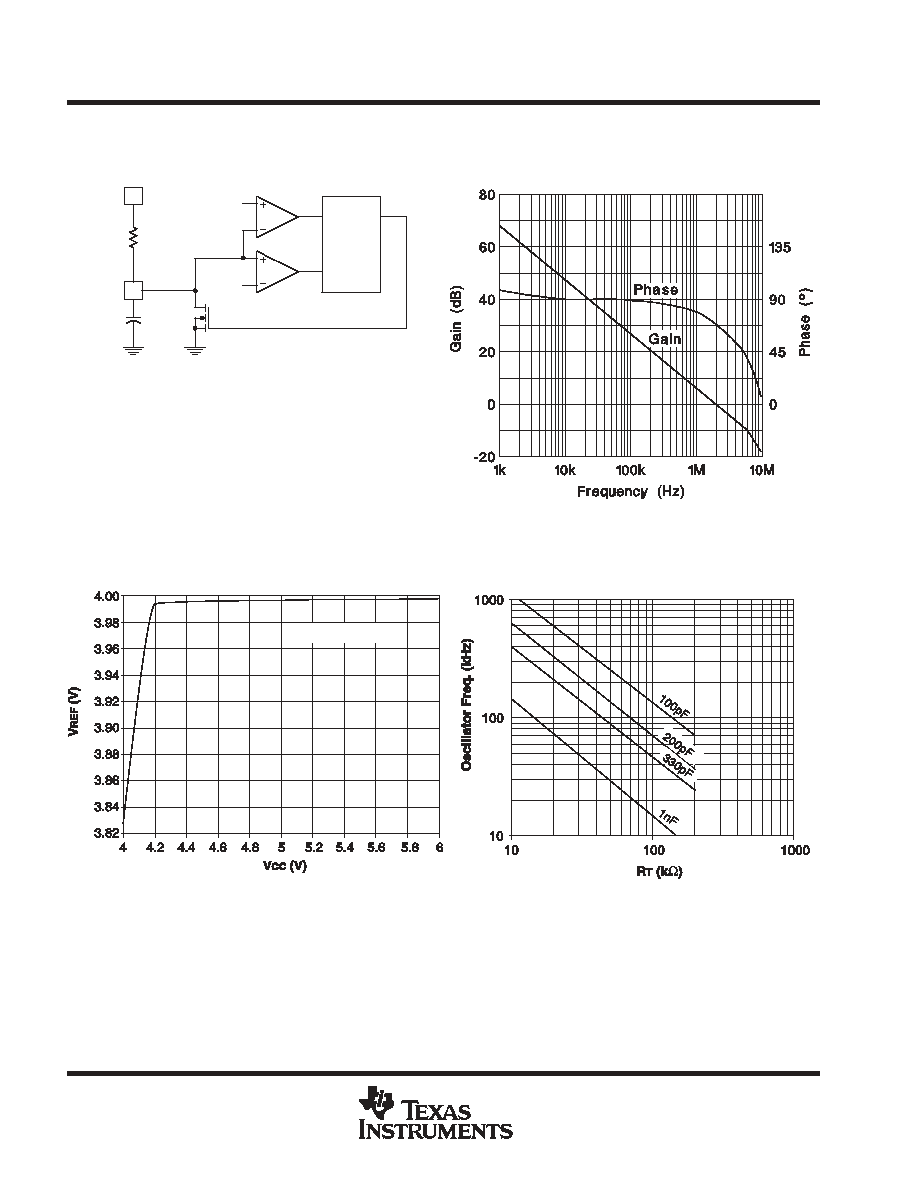
PARAMETER MEASUREMENT INFORMATION
Figure 1
Oscillator
The UCC2813-0/1/2/3/4/5 oscillator generates a sawtooth
waveform on RC. The rise time is set by the time constant of RT and
CT. The fall time is set by CT and an internal transistor
on-resistance of approximately 125. During the fall time, the output
is off and the maximum duty cycle is reduced below 50% or 100%
depending on the part number. Larger timing capacitors increase
the discharge time and reduce the maximum duty cycle and
frequency.
0.2 V
2.5 V
S
R
Q
REF
RC
C
T
R
T
8
4
Figure 2
Error Amplifier
Gain/Phase Response
Figure 3
UCC2813-3/5 V
REF
vs
V
CC
I
LOAD
= 0.5 mA
Figure 4
UCC2813-0/1/2/4 Oscillator Frequency
vs
R
T
and C
T

UCC2813 0/ 1/ 2/ 3/ 4/ 5 Q1
LOW POWER BICMOS CURRENT MODE PWM
SGLS245 - MAY 2004
9
POST OFFICE BOX 655303
∑
DALLAS, TEXAS 75265
Figure 5
UCC2813-3/5 Oscillator Frequency
vs
R
T
and C
T
Figure 6
UCC2813-0/2/3 Maximum Duty Cycle
vs
Oscillator Frequency
Figure 7
UCC2813-1/4/5 Maximum Duty Cycle
vs
Oscillator Frequency
Figure 8
UCC2813-0 I
CC
vs
Oscillator Frequency

UCC2813 0/ 1/ 2/ 3/ 4/ 5 Q1
LOW POWER BICMOS CURRENT MODE PWM
SGLS245 - MAY 2004
10
POST OFFICE BOX 655303
∑
DALLAS, TEXAS 75265
Figure 9
UCC2813-5 I
CC
vs
Oscillator Frequency
Figure 10
Dead Time
vs
C
T
R
T
= 100 k
W
Figure 11
COMP to CS Offset
vs
Temperature
CS = 0 V

PACKAGING INFORMATION
Orderable Device
Status
(1)
Package
Type
Package
Drawing
Pins Package
Qty
Eco Plan
(2)
Lead/Ball Finish
MSL Peak Temp
(3)
UCC2813QDR-0Q1
ACTIVE
SOIC
D
8
2500
None
CU NIPDAU
Level-1-260C-UNLIM
UCC2813QDR-1Q1
ACTIVE
SOIC
D
8
2500
None
CU NIPDAU
Level-1-260C-UNLIM
UCC2813QDR-2Q1
ACTIVE
SOIC
D
8
75
None
CU NIPDAU
Level-1-260C-UNLIM
UCC2813QDR-3Q1
ACTIVE
SOIC
D
8
2500
None
CU NIPDAU
Level-1-260C-UNLIM
UCC2813QDR-4Q1
ACTIVE
SOIC
D
8
2500
None
CU NIPDAU
Level-1-260C-UNLIM
UCC2813QDR-5Q1
ACTIVE
SOIC
D
8
2500
None
CU NIPDAU
Level-1-260C-UNLIM
(1)
The marketing status values are defined as follows:
ACTIVE: Product device recommended for new designs.
LIFEBUY: TI has announced that the device will be discontinued, and a lifetime-buy period is in effect.
NRND: Not recommended for new designs. Device is in production to support existing customers, but TI does not recommend using this part in
a new design.
PREVIEW: Device has been announced but is not in production. Samples may or may not be available.
OBSOLETE: TI has discontinued the production of the device.
(2)
Eco Plan - May not be currently available - please check
http://www.ti.com/productcontent
for the latest availability information and additional
product content details.
None: Not yet available Lead (Pb-Free).
Pb-Free (RoHS): TI's terms "Lead-Free" or "Pb-Free" mean semiconductor products that are compatible with the current RoHS requirements
for all 6 substances, including the requirement that lead not exceed 0.1% by weight in homogeneous materials. Where designed to be soldered
at high temperatures, TI Pb-Free products are suitable for use in specified lead-free processes.
Green (RoHS & no Sb/Br): TI defines "Green" to mean "Pb-Free" and in addition, uses package materials that do not contain halogens,
including bromine (Br) or antimony (Sb) above 0.1% of total product weight.
(3)
MSL, Peak Temp. -- The Moisture Sensitivity Level rating according to the JEDECindustry standard classifications, and peak solder
temperature.
Important Information and Disclaimer:The information provided on this page represents TI's knowledge and belief as of the date that it is
provided. TI bases its knowledge and belief on information provided by third parties, and makes no representation or warranty as to the
accuracy of such information. Efforts are underway to better integrate information from third parties. TI has taken and continues to take
reasonable steps to provide representative and accurate information but may not have conducted destructive testing or chemical analysis on
incoming materials and chemicals. TI and TI suppliers consider certain information to be proprietary, and thus CAS numbers and other limited
information may not be available for release.
In no event shall TI's liability arising out of such information exceed the total purchase price of the TI part(s) at issue in this document sold by TI
to Customer on an annual basis.
PACKAGE OPTION ADDENDUM
www.ti.com
25-Feb-2005
Addendum-Page 1


IMPORTANT NOTICE
Texas Instruments Incorporated and its subsidiaries (TI) reserve the right to make corrections, modifications,
enhancements, improvements, and other changes to its products and services at any time and to discontinue
any product or service without notice. Customers should obtain the latest relevant information before placing
orders and should verify that such information is current and complete. All products are sold subject to TI's terms
and conditions of sale supplied at the time of order acknowledgment.
TI warrants performance of its hardware products to the specifications applicable at the time of sale in
accordance with TI's standard warranty. Testing and other quality control techniques are used to the extent TI
deems necessary to support this warranty. Except where mandated by government requirements, testing of all
parameters of each product is not necessarily performed.
TI assumes no liability for applications assistance or customer product design. Customers are responsible for
their products and applications using TI components. To minimize the risks associated with customer products
and applications, customers should provide adequate design and operating safeguards.
TI does not warrant or represent that any license, either express or implied, is granted under any TI patent right,
copyright, mask work right, or other TI intellectual property right relating to any combination, machine, or process
in which TI products or services are used. Information published by TI regarding third-party products or services
does not constitute a license from TI to use such products or services or a warranty or endorsement thereof.
Use of such information may require a license from a third party under the patents or other intellectual property
of the third party, or a license from TI under the patents or other intellectual property of TI.
Reproduction of information in TI data books or data sheets is permissible only if reproduction is without
alteration and is accompanied by all associated warranties, conditions, limitations, and notices. Reproduction
of this information with alteration is an unfair and deceptive business practice. TI is not responsible or liable for
such altered documentation.
Resale of TI products or services with statements different from or beyond the parameters stated by TI for that
product or service voids all express and any implied warranties for the associated TI product or service and
is an unfair and deceptive business practice. TI is not responsible or liable for any such statements.
Following are URLs where you can obtain information on other Texas Instruments products and application
solutions:
Products
Applications
Amplifiers
amplifier.ti.com
Audio
www.ti.com/audio
Data Converters
dataconverter.ti.com
Automotive
www.ti.com/automotive
DSP
dsp.ti.com
Broadband
www.ti.com/broadband
Interface
interface.ti.com
Digital Control
www.ti.com/digitalcontrol
Logic
logic.ti.com
Military
www.ti.com/military
Power Mgmt
power.ti.com
Optical Networking
www.ti.com/opticalnetwork
Microcontrollers
microcontroller.ti.com
Security
www.ti.com/security
Telephony
www.ti.com/telephony
Video & Imaging
www.ti.com/video
Wireless
www.ti.com/wireless
Mailing Address:
Texas Instruments
Post Office Box 655303 Dallas, Texas 75265
Copyright
2005, Texas Instruments Incorporated